EP0216703B1 - Substrat conducteur et transparent pour élément photoélectrique - Google Patents
Substrat conducteur et transparent pour élément photoélectrique Download PDFInfo
- Publication number
- EP0216703B1 EP0216703B1 EP86402059A EP86402059A EP0216703B1 EP 0216703 B1 EP0216703 B1 EP 0216703B1 EP 86402059 A EP86402059 A EP 86402059A EP 86402059 A EP86402059 A EP 86402059A EP 0216703 B1 EP0216703 B1 EP 0216703B1
- Authority
- EP
- European Patent Office
- Prior art keywords
- tin
- support
- thickness
- transparent
- conductive
- Prior art date
- Legal status (The legal status is an assumption and is not a legal conclusion. Google has not performed a legal analysis and makes no representation as to the accuracy of the status listed.)
- Expired - Lifetime
Links
- 239000000758 substrate Substances 0.000 title claims abstract description 23
- XOLBLPGZBRYERU-UHFFFAOYSA-N tin dioxide Chemical compound O=[Sn]=O XOLBLPGZBRYERU-UHFFFAOYSA-N 0.000 claims abstract description 27
- ZAMOUSCENKQFHK-UHFFFAOYSA-N Chlorine atom Chemical compound [Cl] ZAMOUSCENKQFHK-UHFFFAOYSA-N 0.000 claims abstract description 15
- 229910052801 chlorine Inorganic materials 0.000 claims abstract description 15
- 239000000460 chlorine Substances 0.000 claims abstract description 15
- 150000003606 tin compounds Chemical class 0.000 claims abstract description 11
- 239000011521 glass Substances 0.000 claims abstract description 10
- 229910052736 halogen Inorganic materials 0.000 claims abstract description 6
- 150000002367 halogens Chemical class 0.000 claims abstract description 6
- 230000003647 oxidation Effects 0.000 claims abstract description 5
- 238000007254 oxidation reaction Methods 0.000 claims abstract description 5
- 238000005979 thermal decomposition reaction Methods 0.000 claims abstract description 4
- 229910021417 amorphous silicon Inorganic materials 0.000 claims description 8
- 150000001875 compounds Chemical class 0.000 claims description 7
- XAGFODPZIPBFFR-UHFFFAOYSA-N aluminium Chemical compound [Al] XAGFODPZIPBFFR-UHFFFAOYSA-N 0.000 claims description 6
- 229910052782 aluminium Inorganic materials 0.000 claims description 6
- VYPSYNLAJGMNEJ-UHFFFAOYSA-N Silicium dioxide Chemical compound O=[Si]=O VYPSYNLAJGMNEJ-UHFFFAOYSA-N 0.000 claims description 4
- 239000004411 aluminium Substances 0.000 claims description 3
- HPGGPRDJHPYFRM-UHFFFAOYSA-J tin(iv) chloride Chemical compound Cl[Sn](Cl)(Cl)Cl HPGGPRDJHPYFRM-UHFFFAOYSA-J 0.000 claims description 3
- ATJFFYVFTNAWJD-UHFFFAOYSA-N Tin Chemical compound [Sn] ATJFFYVFTNAWJD-UHFFFAOYSA-N 0.000 claims description 2
- 229910021627 Tin(IV) chloride Inorganic materials 0.000 claims description 2
- 239000000377 silicon dioxide Substances 0.000 claims description 2
- OLGIDLDDXHSYFE-UHFFFAOYSA-N dihydridotin Chemical compound [SnH2] OLGIDLDDXHSYFE-UHFFFAOYSA-N 0.000 claims 1
- 125000002496 methyl group Chemical group [H]C([H])([H])* 0.000 claims 1
- 229910001887 tin oxide Inorganic materials 0.000 abstract description 17
- 238000004519 manufacturing process Methods 0.000 abstract description 2
- 238000006243 chemical reaction Methods 0.000 description 8
- YCKRFDGAMUMZLT-UHFFFAOYSA-N Fluorine atom Chemical compound [F] YCKRFDGAMUMZLT-UHFFFAOYSA-N 0.000 description 6
- 229910052731 fluorine Inorganic materials 0.000 description 6
- 239000011737 fluorine Substances 0.000 description 6
- 238000000034 method Methods 0.000 description 6
- BLRPTPMANUNPDV-UHFFFAOYSA-N Silane Chemical compound [SiH4] BLRPTPMANUNPDV-UHFFFAOYSA-N 0.000 description 4
- XUIMIQQOPSSXEZ-UHFFFAOYSA-N Silicon Chemical compound [Si] XUIMIQQOPSSXEZ-UHFFFAOYSA-N 0.000 description 4
- 239000007789 gas Substances 0.000 description 4
- IJGRMHOSHXDMSA-UHFFFAOYSA-N Atomic nitrogen Chemical compound N#N IJGRMHOSHXDMSA-UHFFFAOYSA-N 0.000 description 3
- 239000004065 semiconductor Substances 0.000 description 3
- 229910052710 silicon Inorganic materials 0.000 description 3
- OAICVXFJPJFONN-UHFFFAOYSA-N Phosphorus Chemical compound [P] OAICVXFJPJFONN-UHFFFAOYSA-N 0.000 description 2
- 230000005540 biological transmission Effects 0.000 description 2
- 238000005229 chemical vapour deposition Methods 0.000 description 2
- 238000000151 deposition Methods 0.000 description 2
- 230000008021 deposition Effects 0.000 description 2
- 238000000197 pyrolysis Methods 0.000 description 2
- 239000010703 silicon Substances 0.000 description 2
- 238000009834 vaporization Methods 0.000 description 2
- XLYOFNOQVPJJNP-UHFFFAOYSA-N water Chemical compound O XLYOFNOQVPJJNP-UHFFFAOYSA-N 0.000 description 2
- ZOXJGFHDIHLPTG-UHFFFAOYSA-N Boron Chemical compound [B] ZOXJGFHDIHLPTG-UHFFFAOYSA-N 0.000 description 1
- -1 HCl Chemical compound 0.000 description 1
- 241001639412 Verres Species 0.000 description 1
- QYFZCTDKWGVUIO-UHFFFAOYSA-N [Cl].[Sn] Chemical class [Cl].[Sn] QYFZCTDKWGVUIO-UHFFFAOYSA-N 0.000 description 1
- QVGXLLKOCUKJST-UHFFFAOYSA-N atomic oxygen Chemical compound [O] QVGXLLKOCUKJST-UHFFFAOYSA-N 0.000 description 1
- 229910052796 boron Inorganic materials 0.000 description 1
- YMLFYGFCXGNERH-UHFFFAOYSA-K butyltin trichloride Chemical compound CCCC[Sn](Cl)(Cl)Cl YMLFYGFCXGNERH-UHFFFAOYSA-K 0.000 description 1
- 230000008878 coupling Effects 0.000 description 1
- 238000010168 coupling process Methods 0.000 description 1
- 238000005859 coupling reaction Methods 0.000 description 1
- 239000013078 crystal Substances 0.000 description 1
- 238000000354 decomposition reaction Methods 0.000 description 1
- 230000003247 decreasing effect Effects 0.000 description 1
- REOJLIXKJWXUGB-UHFFFAOYSA-N mofebutazone Chemical group O=C1C(CCCC)C(=O)NN1C1=CC=CC=C1 REOJLIXKJWXUGB-UHFFFAOYSA-N 0.000 description 1
- 229910052757 nitrogen Inorganic materials 0.000 description 1
- 239000001301 oxygen Substances 0.000 description 1
- 229910052760 oxygen Inorganic materials 0.000 description 1
- 239000000843 powder Substances 0.000 description 1
- 239000002994 raw material Substances 0.000 description 1
- 239000005361 soda-lime glass Substances 0.000 description 1
- 238000005507 spraying Methods 0.000 description 1
Images
Classifications
-
- H—ELECTRICITY
- H10—SEMICONDUCTOR DEVICES; ELECTRIC SOLID-STATE DEVICES NOT OTHERWISE PROVIDED FOR
- H10F—INORGANIC SEMICONDUCTOR DEVICES SENSITIVE TO INFRARED RADIATION, LIGHT, ELECTROMAGNETIC RADIATION OF SHORTER WAVELENGTH OR CORPUSCULAR RADIATION
- H10F77/00—Constructional details of devices covered by this subclass
- H10F77/10—Semiconductor bodies
- H10F77/16—Material structures, e.g. crystalline structures, film structures or crystal plane orientations
- H10F77/169—Thin semiconductor films on metallic or insulating substrates
- H10F77/1692—Thin semiconductor films on metallic or insulating substrates the films including only Group IV materials
-
- C—CHEMISTRY; METALLURGY
- C03—GLASS; MINERAL OR SLAG WOOL
- C03C—CHEMICAL COMPOSITION OF GLASSES, GLAZES OR VITREOUS ENAMELS; SURFACE TREATMENT OF GLASS; SURFACE TREATMENT OF FIBRES OR FILAMENTS MADE FROM GLASS, MINERALS OR SLAGS; JOINING GLASS TO GLASS OR OTHER MATERIALS
- C03C17/00—Surface treatment of glass, not in the form of fibres or filaments, by coating
- C03C17/22—Surface treatment of glass, not in the form of fibres or filaments, by coating with other inorganic material
- C03C17/23—Oxides
- C03C17/245—Oxides by deposition from the vapour phase
- C03C17/2453—Coating containing SnO2
-
- H—ELECTRICITY
- H10—SEMICONDUCTOR DEVICES; ELECTRIC SOLID-STATE DEVICES NOT OTHERWISE PROVIDED FOR
- H10F—INORGANIC SEMICONDUCTOR DEVICES SENSITIVE TO INFRARED RADIATION, LIGHT, ELECTROMAGNETIC RADIATION OF SHORTER WAVELENGTH OR CORPUSCULAR RADIATION
- H10F71/00—Manufacture or treatment of devices covered by this subclass
- H10F71/138—Manufacture of transparent electrodes, e.g. transparent conductive oxides [TCO] or indium tin oxide [ITO] electrodes
-
- Y—GENERAL TAGGING OF NEW TECHNOLOGICAL DEVELOPMENTS; GENERAL TAGGING OF CROSS-SECTIONAL TECHNOLOGIES SPANNING OVER SEVERAL SECTIONS OF THE IPC; TECHNICAL SUBJECTS COVERED BY FORMER USPC CROSS-REFERENCE ART COLLECTIONS [XRACs] AND DIGESTS
- Y02—TECHNOLOGIES OR APPLICATIONS FOR MITIGATION OR ADAPTATION AGAINST CLIMATE CHANGE
- Y02E—REDUCTION OF GREENHOUSE GAS [GHG] EMISSIONS, RELATED TO ENERGY GENERATION, TRANSMISSION OR DISTRIBUTION
- Y02E10/00—Energy generation through renewable energy sources
- Y02E10/50—Photovoltaic [PV] energy
Definitions
- the present invention relates to a substrate which is both conductive and transparent for a photoelectric element consisting for example of a glass plate coated with a conductive and transparent layer based on tin oxide, this element being usable in particular in cells or solar cells.
- solar cells having as photoelectric element a transparent conductive substrate coated with amorphous silicon a-Si and provided with aluminum electrodes. Such solar cells have a low photoelectric conversion rate and to improve it we have sought to make the substrate as conductive as possible by doping the tin oxide layer with fluorine.
- the present invention aims to solve this problem and to provide a transparent substrate, in particular made of glass, coated with a layer based on tin oxide, usable as a photoelectric element in particular in solar cells, and making it possible to '' achieve high photoelectric conversion rates, higher than those obtained with photoelectric elements whose tin oxide layer is doped with fluorine.
- a transparent substrate consisting of a support, in particular made of glass, coated with a conductive and transparent layer based on tin oxide obtained by thermal decomposition and oxidation in contact with the support brought to high temperature, d '' a tin compound containing chlorine but no other halogen, or a tin compound without chlorine but to which is added in addition another compound containing chlorine such as HCl, this conductive layer, based on tin oxide having a thickness at least equal to 0.7 micron.
- Tin compounds containing chlorine, and no other halogen than chlorine are however preferable to non-chlorine tin compounds to which a chlorine-containing compound such as HCl is added in addition.
- the C.V.D. method can be used. (Chemical Vapor Deposition) consisting in bringing a vapor of these compounds into contact with the heated support, the method of pyrolysis of solution consisting in spraying a solution of these compounds on the heated support, or any other method, in particular the method of pyrolysis powder.
- the C.V.D. method is preferably used, advantageous in particular for its flexibility of use and the quality of the deposit obtained.
- the transparent support, in particular the glass is then heated to a temperature of the order of 400 to 600 ° C.
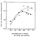
- the expected thickness of the conductive layer of tin oxide is at least 0.7 micron, but preferably, to further improve the photoelectric conversion rate, it is of the order of 0.8 to 1.2 microns.
- Solar cells were produced on the one hand from conductive substrates according to the invention, on the other hand from conventional substrates and performance comparisons were made.
- the batteries produced from substrates "A” have a better energy conversion rate than those manufactured from substrates "B".
- the electrical resistance is slightly lowered, due to the thickness on the one hand, and the fact that the size of the crystals formed is increased, which favorably modifies the surface condition of the layer, on the other hand.
Landscapes
- Chemical & Material Sciences (AREA)
- Materials Engineering (AREA)
- Engineering & Computer Science (AREA)
- Chemical Kinetics & Catalysis (AREA)
- General Chemical & Material Sciences (AREA)
- Geochemistry & Mineralogy (AREA)
- Life Sciences & Earth Sciences (AREA)
- Organic Chemistry (AREA)
- Photovoltaic Devices (AREA)
- Non-Insulated Conductors (AREA)
- Manufacturing Of Electric Cables (AREA)
- Surface Treatment Of Glass (AREA)
- Liquid Crystal (AREA)
Priority Applications (1)
| Application Number | Priority Date | Filing Date | Title |
|---|---|---|---|
| AT86402059T ATE71925T1 (de) | 1985-09-20 | 1986-09-19 | Leitfaehiges und durchsichtiges substrat fuer ein photoelektrisches element. |
Applications Claiming Priority (2)
| Application Number | Priority Date | Filing Date | Title |
|---|---|---|---|
| JP60208363A JPS6269405A (ja) | 1985-09-20 | 1985-09-20 | 光電素子用透明導電基板 |
| JP208363/85 | 1985-09-20 |
Publications (3)
| Publication Number | Publication Date |
|---|---|
| EP0216703A2 EP0216703A2 (fr) | 1987-04-01 |
| EP0216703A3 EP0216703A3 (en) | 1989-04-26 |
| EP0216703B1 true EP0216703B1 (fr) | 1992-01-22 |
Family
ID=16555049
Family Applications (1)
| Application Number | Title | Priority Date | Filing Date |
|---|---|---|---|
| EP86402059A Expired - Lifetime EP0216703B1 (fr) | 1985-09-20 | 1986-09-19 | Substrat conducteur et transparent pour élément photoélectrique |
Country Status (5)
| Country | Link |
|---|---|
| EP (1) | EP0216703B1 (enExample) |
| JP (1) | JPS6269405A (enExample) |
| AT (1) | ATE71925T1 (enExample) |
| DE (1) | DE3683575D1 (enExample) |
| ES (1) | ES2003352A6 (enExample) |
Families Citing this family (5)
| Publication number | Priority date | Publication date | Assignee | Title |
|---|---|---|---|---|
| JPH07112076B2 (ja) * | 1987-05-07 | 1995-11-29 | 日本板硝子株式会社 | 二層構造を有する透明導電膜体 |
| JP2853125B2 (ja) * | 1988-03-17 | 1999-02-03 | 日本板硝子株式会社 | 透明導電膜の製造方法 |
| DE19715048C2 (de) * | 1997-04-11 | 1999-08-19 | Bosch Gmbh Robert | Verfahren zum Strukturieren einer transparenten, elektrisch leitfähigen Schicht |
| US6602606B1 (en) * | 1999-05-18 | 2003-08-05 | Nippon Sheet Glass Co., Ltd. | Glass sheet with conductive film, method of manufacturing the same, and photoelectric conversion device using the same |
| CN104310790A (zh) * | 2014-09-28 | 2015-01-28 | 中国建材国际工程集团有限公司 | 大面积透明导电膜玻璃的制备方法 |
Family Cites Families (3)
| Publication number | Priority date | Publication date | Assignee | Title |
|---|---|---|---|---|
| JPS5534668A (en) * | 1978-09-04 | 1980-03-11 | Toshiba Corp | Forming method for transparent conductive composite film |
| JPS59136477A (ja) * | 1982-12-23 | 1984-08-06 | Nippon Sheet Glass Co Ltd | 基体に酸化錫膜を形成する方法 |
| JPS59162269A (ja) * | 1983-03-07 | 1984-09-13 | Nippon Sheet Glass Co Ltd | 基体に酸化錫膜を形成する方法 |
-
1985
- 1985-09-20 JP JP60208363A patent/JPS6269405A/ja active Granted
-
1986
- 1986-09-19 AT AT86402059T patent/ATE71925T1/de not_active IP Right Cessation
- 1986-09-19 EP EP86402059A patent/EP0216703B1/fr not_active Expired - Lifetime
- 1986-09-19 ES ES8602025A patent/ES2003352A6/es not_active Expired - Fee Related
- 1986-09-19 DE DE8686402059T patent/DE3683575D1/de not_active Expired - Fee Related
Also Published As
| Publication number | Publication date |
|---|---|
| DE3683575D1 (de) | 1992-03-05 |
| ATE71925T1 (de) | 1992-02-15 |
| EP0216703A3 (en) | 1989-04-26 |
| EP0216703A2 (fr) | 1987-04-01 |
| JPH0572686B2 (enExample) | 1993-10-12 |
| JPS6269405A (ja) | 1987-03-30 |
| ES2003352A6 (es) | 1991-03-16 |
Similar Documents
| Publication | Publication Date | Title |
|---|---|---|
| US9059370B2 (en) | Zinc oxide film method and structure for CIGS cell | |
| US6734352B2 (en) | Photoelectric conversion device | |
| CA1318193C (fr) | Fabrication d'un conducteur electrique transparent | |
| AU2005200023B2 (en) | Photovoltaic device | |
| JP2846651B2 (ja) | 光起電力装置 | |
| US6512170B1 (en) | Photoelectric conversion device | |
| EP0216703B1 (fr) | Substrat conducteur et transparent pour élément photoélectrique | |
| EP0335769A2 (fr) | Verre électroconducteur et procédé pour sa fabrication | |
| JP2009117463A (ja) | 薄膜光電変換装置 | |
| Moustakas et al. | Effect of phosphorus and boron impurities on amorphous silicon solar cells | |
| EP0382632B1 (fr) | Substrat transparent électroconducteur à deux couches d'oxydes métalliques, utile notamment dans des dispositifs opto-électroniques | |
| JP2003188400A (ja) | 結晶性SiC膜の製造方法、結晶性SiC膜及び太陽電池 | |
| US5278015A (en) | Amorphous silicon film, its production and photo semiconductor device utilizing such a film | |
| JP4187328B2 (ja) | 光起電力素子の製造方法 | |
| EP0290345B1 (fr) | Film électroconducteur pour élément photovoltaique | |
| JP2002237610A (ja) | 光電変換装置およびその製造方法 | |
| JPWO2005109526A1 (ja) | 薄膜光電変換装置 | |
| US5152833A (en) | Amorphous silicon film, its production and photo semiconductor device utilizing such a film | |
| JPH0121634B2 (enExample) | ||
| EP2104145A1 (fr) | Substrat de type verrier revêtu de couches minces et procédé de fabrication | |
| JP5160574B2 (ja) | 光電変換装置 | |
| Osborne et al. | Stable hydrogenated amorphous silicon films deposited from silane and dichlorosilane by radio frequency plasma chemical vapor deposition | |
| US5258207A (en) | Amorphous silicon film, its production and photo semiconductor device utilizing such a film | |
| JP2822358B2 (ja) | 薄膜太陽電池の製造方法 | |
| FR2573249A1 (fr) | Procede pour la preparation d'elements semi-conducteurs a couches minces, et en particulier de cellules solaires |
Legal Events
| Date | Code | Title | Description |
|---|---|---|---|
| PUAI | Public reference made under article 153(3) epc to a published international application that has entered the european phase |
Free format text: ORIGINAL CODE: 0009012 |
|
| AK | Designated contracting states |
Kind code of ref document: A2 Designated state(s): AT BE CH DE FR GB IT LI LU NL SE |
|
| PUAL | Search report despatched |
Free format text: ORIGINAL CODE: 0009013 |
|
| AK | Designated contracting states |
Kind code of ref document: A3 Designated state(s): AT BE CH DE FR GB IT LI LU NL SE |
|
| 17P | Request for examination filed |
Effective date: 19890920 |
|
| RAP1 | Party data changed (applicant data changed or rights of an application transferred) |
Owner name: SAINT-GOBAIN VITRAGE INTERNATIONAL |
|
| 17Q | First examination report despatched |
Effective date: 19900829 |
|
| GRAA | (expected) grant |
Free format text: ORIGINAL CODE: 0009210 |
|
| AK | Designated contracting states |
Kind code of ref document: B1 Designated state(s): AT BE CH DE FR GB IT LI LU NL SE |
|
| REF | Corresponds to: |
Ref document number: 71925 Country of ref document: AT Date of ref document: 19920215 Kind code of ref document: T |
|
| REF | Corresponds to: |
Ref document number: 3683575 Country of ref document: DE Date of ref document: 19920305 |
|
| ITF | It: translation for a ep patent filed | ||
| GBT | Gb: translation of ep patent filed (gb section 77(6)(a)/1977) | ||
| PLBE | No opposition filed within time limit |
Free format text: ORIGINAL CODE: 0009261 |
|
| STAA | Information on the status of an ep patent application or granted ep patent |
Free format text: STATUS: NO OPPOSITION FILED WITHIN TIME LIMIT |
|
| 26N | No opposition filed | ||
| EPTA | Lu: last paid annual fee | ||
| EAL | Se: european patent in force in sweden |
Ref document number: 86402059.9 |
|
| PGFP | Annual fee paid to national office [announced via postgrant information from national office to epo] |
Ref country code: SE Payment date: 19980810 Year of fee payment: 13 |
|
| PGFP | Annual fee paid to national office [announced via postgrant information from national office to epo] |
Ref country code: GB Payment date: 19980825 Year of fee payment: 13 |
|
| PGFP | Annual fee paid to national office [announced via postgrant information from national office to epo] |
Ref country code: AT Payment date: 19980909 Year of fee payment: 13 |
|
| PGFP | Annual fee paid to national office [announced via postgrant information from national office to epo] |
Ref country code: FR Payment date: 19980910 Year of fee payment: 13 |
|
| PGFP | Annual fee paid to national office [announced via postgrant information from national office to epo] |
Ref country code: BE Payment date: 19980915 Year of fee payment: 13 |
|
| PGFP | Annual fee paid to national office [announced via postgrant information from national office to epo] |
Ref country code: NL Payment date: 19980930 Year of fee payment: 13 |
|
| PGFP | Annual fee paid to national office [announced via postgrant information from national office to epo] |
Ref country code: DE Payment date: 19981010 Year of fee payment: 13 |
|
| PGFP | Annual fee paid to national office [announced via postgrant information from national office to epo] |
Ref country code: LU Payment date: 19981023 Year of fee payment: 13 |
|
| PGFP | Annual fee paid to national office [announced via postgrant information from national office to epo] |
Ref country code: CH Payment date: 19981221 Year of fee payment: 13 |
|
| PG25 | Lapsed in a contracting state [announced via postgrant information from national office to epo] |
Ref country code: LU Free format text: LAPSE BECAUSE OF NON-PAYMENT OF DUE FEES Effective date: 19990919 Ref country code: GB Free format text: LAPSE BECAUSE OF NON-PAYMENT OF DUE FEES Effective date: 19990919 Ref country code: AT Free format text: LAPSE BECAUSE OF NON-PAYMENT OF DUE FEES Effective date: 19990919 |
|
| PG25 | Lapsed in a contracting state [announced via postgrant information from national office to epo] |
Ref country code: SE Free format text: THE PATENT HAS BEEN ANNULLED BY A DECISION OF A NATIONAL AUTHORITY Effective date: 19990929 |
|
| PG25 | Lapsed in a contracting state [announced via postgrant information from national office to epo] |
Ref country code: LI Free format text: LAPSE BECAUSE OF NON-PAYMENT OF DUE FEES Effective date: 19990930 Ref country code: CH Free format text: LAPSE BECAUSE OF NON-PAYMENT OF DUE FEES Effective date: 19990930 Ref country code: BE Free format text: LAPSE BECAUSE OF NON-PAYMENT OF DUE FEES Effective date: 19990930 |
|
| BERE | Be: lapsed |
Owner name: SAINT-GOBAIN VITRAGE INTERNATIONAL Effective date: 19990930 |
|
| PG25 | Lapsed in a contracting state [announced via postgrant information from national office to epo] |
Ref country code: NL Free format text: LAPSE BECAUSE OF NON-PAYMENT OF DUE FEES Effective date: 20000401 |
|
| GBPC | Gb: european patent ceased through non-payment of renewal fee |
Effective date: 19990919 |
|
| EUG | Se: european patent has lapsed |
Ref document number: 86402059.9 |
|
| REG | Reference to a national code |
Ref country code: CH Ref legal event code: PL |
|
| PG25 | Lapsed in a contracting state [announced via postgrant information from national office to epo] |
Ref country code: FR Free format text: LAPSE BECAUSE OF NON-PAYMENT OF DUE FEES Effective date: 20000531 |
|
| NLV4 | Nl: lapsed or anulled due to non-payment of the annual fee |
Effective date: 20000401 |
|
| PG25 | Lapsed in a contracting state [announced via postgrant information from national office to epo] |
Ref country code: DE Free format text: LAPSE BECAUSE OF NON-PAYMENT OF DUE FEES Effective date: 20000701 |
|
| REG | Reference to a national code |
Ref country code: FR Ref legal event code: ST |
|
| PG25 | Lapsed in a contracting state [announced via postgrant information from national office to epo] |
Ref country code: IT Free format text: LAPSE BECAUSE OF NON-PAYMENT OF DUE FEES Effective date: 20050919 |