EP0216703B1 - Conducting and transparent substrate for a photoelectric element - Google Patents
Conducting and transparent substrate for a photoelectric element Download PDFInfo
- Publication number
- EP0216703B1 EP0216703B1 EP86402059A EP86402059A EP0216703B1 EP 0216703 B1 EP0216703 B1 EP 0216703B1 EP 86402059 A EP86402059 A EP 86402059A EP 86402059 A EP86402059 A EP 86402059A EP 0216703 B1 EP0216703 B1 EP 0216703B1
- Authority
- EP
- European Patent Office
- Prior art keywords
- tin
- support
- thickness
- transparent
- conductive
- Prior art date
- Legal status (The legal status is an assumption and is not a legal conclusion. Google has not performed a legal analysis and makes no representation as to the accuracy of the status listed.)
- Expired - Lifetime
Links
- 239000000758 substrate Substances 0.000 title claims abstract description 23
- XOLBLPGZBRYERU-UHFFFAOYSA-N tin dioxide Chemical compound O=[Sn]=O XOLBLPGZBRYERU-UHFFFAOYSA-N 0.000 claims abstract description 27
- ZAMOUSCENKQFHK-UHFFFAOYSA-N Chlorine atom Chemical compound [Cl] ZAMOUSCENKQFHK-UHFFFAOYSA-N 0.000 claims abstract description 15
- 229910052801 chlorine Inorganic materials 0.000 claims abstract description 15
- 239000000460 chlorine Substances 0.000 claims abstract description 15
- 150000003606 tin compounds Chemical class 0.000 claims abstract description 11
- 239000011521 glass Substances 0.000 claims abstract description 10
- 229910052736 halogen Inorganic materials 0.000 claims abstract description 6
- 150000002367 halogens Chemical class 0.000 claims abstract description 6
- 230000003647 oxidation Effects 0.000 claims abstract description 5
- 238000007254 oxidation reaction Methods 0.000 claims abstract description 5
- 238000005979 thermal decomposition reaction Methods 0.000 claims abstract description 4
- 229910021417 amorphous silicon Inorganic materials 0.000 claims description 8
- 150000001875 compounds Chemical class 0.000 claims description 7
- XAGFODPZIPBFFR-UHFFFAOYSA-N aluminium Chemical compound [Al] XAGFODPZIPBFFR-UHFFFAOYSA-N 0.000 claims description 6
- 229910052782 aluminium Inorganic materials 0.000 claims description 6
- VYPSYNLAJGMNEJ-UHFFFAOYSA-N Silicium dioxide Chemical compound O=[Si]=O VYPSYNLAJGMNEJ-UHFFFAOYSA-N 0.000 claims description 4
- 239000004411 aluminium Substances 0.000 claims description 3
- HPGGPRDJHPYFRM-UHFFFAOYSA-J tin(iv) chloride Chemical compound Cl[Sn](Cl)(Cl)Cl HPGGPRDJHPYFRM-UHFFFAOYSA-J 0.000 claims description 3
- ATJFFYVFTNAWJD-UHFFFAOYSA-N Tin Chemical compound [Sn] ATJFFYVFTNAWJD-UHFFFAOYSA-N 0.000 claims description 2
- 229910021627 Tin(IV) chloride Inorganic materials 0.000 claims description 2
- 239000000377 silicon dioxide Substances 0.000 claims description 2
- OLGIDLDDXHSYFE-UHFFFAOYSA-N dihydridotin Chemical compound [SnH2] OLGIDLDDXHSYFE-UHFFFAOYSA-N 0.000 claims 1
- 125000002496 methyl group Chemical group [H]C([H])([H])* 0.000 claims 1
- 229910001887 tin oxide Inorganic materials 0.000 abstract description 17
- 238000004519 manufacturing process Methods 0.000 abstract description 2
- 238000006243 chemical reaction Methods 0.000 description 8
- YCKRFDGAMUMZLT-UHFFFAOYSA-N Fluorine atom Chemical compound [F] YCKRFDGAMUMZLT-UHFFFAOYSA-N 0.000 description 6
- 229910052731 fluorine Inorganic materials 0.000 description 6
- 239000011737 fluorine Substances 0.000 description 6
- 238000000034 method Methods 0.000 description 6
- BLRPTPMANUNPDV-UHFFFAOYSA-N Silane Chemical compound [SiH4] BLRPTPMANUNPDV-UHFFFAOYSA-N 0.000 description 4
- XUIMIQQOPSSXEZ-UHFFFAOYSA-N Silicon Chemical compound [Si] XUIMIQQOPSSXEZ-UHFFFAOYSA-N 0.000 description 4
- 239000007789 gas Substances 0.000 description 4
- IJGRMHOSHXDMSA-UHFFFAOYSA-N Atomic nitrogen Chemical compound N#N IJGRMHOSHXDMSA-UHFFFAOYSA-N 0.000 description 3
- 239000004065 semiconductor Substances 0.000 description 3
- 229910052710 silicon Inorganic materials 0.000 description 3
- OAICVXFJPJFONN-UHFFFAOYSA-N Phosphorus Chemical compound [P] OAICVXFJPJFONN-UHFFFAOYSA-N 0.000 description 2
- 230000005540 biological transmission Effects 0.000 description 2
- 238000005229 chemical vapour deposition Methods 0.000 description 2
- 238000000151 deposition Methods 0.000 description 2
- 230000008021 deposition Effects 0.000 description 2
- 238000000197 pyrolysis Methods 0.000 description 2
- 239000010703 silicon Substances 0.000 description 2
- 238000009834 vaporization Methods 0.000 description 2
- XLYOFNOQVPJJNP-UHFFFAOYSA-N water Chemical compound O XLYOFNOQVPJJNP-UHFFFAOYSA-N 0.000 description 2
- ZOXJGFHDIHLPTG-UHFFFAOYSA-N Boron Chemical compound [B] ZOXJGFHDIHLPTG-UHFFFAOYSA-N 0.000 description 1
- -1 HCl Chemical compound 0.000 description 1
- 241001639412 Verres Species 0.000 description 1
- QYFZCTDKWGVUIO-UHFFFAOYSA-N [Cl].[Sn] Chemical class [Cl].[Sn] QYFZCTDKWGVUIO-UHFFFAOYSA-N 0.000 description 1
- QVGXLLKOCUKJST-UHFFFAOYSA-N atomic oxygen Chemical compound [O] QVGXLLKOCUKJST-UHFFFAOYSA-N 0.000 description 1
- 229910052796 boron Inorganic materials 0.000 description 1
- YMLFYGFCXGNERH-UHFFFAOYSA-K butyltin trichloride Chemical compound CCCC[Sn](Cl)(Cl)Cl YMLFYGFCXGNERH-UHFFFAOYSA-K 0.000 description 1
- 230000008878 coupling Effects 0.000 description 1
- 238000010168 coupling process Methods 0.000 description 1
- 238000005859 coupling reaction Methods 0.000 description 1
- 239000013078 crystal Substances 0.000 description 1
- 238000000354 decomposition reaction Methods 0.000 description 1
- 230000003247 decreasing effect Effects 0.000 description 1
- REOJLIXKJWXUGB-UHFFFAOYSA-N mofebutazone Chemical group O=C1C(CCCC)C(=O)NN1C1=CC=CC=C1 REOJLIXKJWXUGB-UHFFFAOYSA-N 0.000 description 1
- 229910052757 nitrogen Inorganic materials 0.000 description 1
- 239000001301 oxygen Substances 0.000 description 1
- 229910052760 oxygen Inorganic materials 0.000 description 1
- 239000000843 powder Substances 0.000 description 1
- 239000002994 raw material Substances 0.000 description 1
- 239000005361 soda-lime glass Substances 0.000 description 1
- 238000005507 spraying Methods 0.000 description 1
Images
Classifications
-
- H—ELECTRICITY
- H01—ELECTRIC ELEMENTS
- H01L—SEMICONDUCTOR DEVICES NOT COVERED BY CLASS H10
- H01L31/00—Semiconductor devices sensitive to infrared radiation, light, electromagnetic radiation of shorter wavelength or corpuscular radiation and specially adapted either for the conversion of the energy of such radiation into electrical energy or for the control of electrical energy by such radiation; Processes or apparatus specially adapted for the manufacture or treatment thereof or of parts thereof; Details thereof
- H01L31/0248—Semiconductor devices sensitive to infrared radiation, light, electromagnetic radiation of shorter wavelength or corpuscular radiation and specially adapted either for the conversion of the energy of such radiation into electrical energy or for the control of electrical energy by such radiation; Processes or apparatus specially adapted for the manufacture or treatment thereof or of parts thereof; Details thereof characterised by their semiconductor bodies
- H01L31/036—Semiconductor devices sensitive to infrared radiation, light, electromagnetic radiation of shorter wavelength or corpuscular radiation and specially adapted either for the conversion of the energy of such radiation into electrical energy or for the control of electrical energy by such radiation; Processes or apparatus specially adapted for the manufacture or treatment thereof or of parts thereof; Details thereof characterised by their semiconductor bodies characterised by their crystalline structure or particular orientation of the crystalline planes
- H01L31/0392—Semiconductor devices sensitive to infrared radiation, light, electromagnetic radiation of shorter wavelength or corpuscular radiation and specially adapted either for the conversion of the energy of such radiation into electrical energy or for the control of electrical energy by such radiation; Processes or apparatus specially adapted for the manufacture or treatment thereof or of parts thereof; Details thereof characterised by their semiconductor bodies characterised by their crystalline structure or particular orientation of the crystalline planes including thin films deposited on metallic or insulating substrates ; characterised by specific substrate materials or substrate features or by the presence of intermediate layers, e.g. barrier layers, on the substrate
- H01L31/03921—Semiconductor devices sensitive to infrared radiation, light, electromagnetic radiation of shorter wavelength or corpuscular radiation and specially adapted either for the conversion of the energy of such radiation into electrical energy or for the control of electrical energy by such radiation; Processes or apparatus specially adapted for the manufacture or treatment thereof or of parts thereof; Details thereof characterised by their semiconductor bodies characterised by their crystalline structure or particular orientation of the crystalline planes including thin films deposited on metallic or insulating substrates ; characterised by specific substrate materials or substrate features or by the presence of intermediate layers, e.g. barrier layers, on the substrate including only elements of Group IV of the Periodic Table
-
- C—CHEMISTRY; METALLURGY
- C03—GLASS; MINERAL OR SLAG WOOL
- C03C—CHEMICAL COMPOSITION OF GLASSES, GLAZES OR VITREOUS ENAMELS; SURFACE TREATMENT OF GLASS; SURFACE TREATMENT OF FIBRES OR FILAMENTS MADE FROM GLASS, MINERALS OR SLAGS; JOINING GLASS TO GLASS OR OTHER MATERIALS
- C03C17/00—Surface treatment of glass, not in the form of fibres or filaments, by coating
- C03C17/22—Surface treatment of glass, not in the form of fibres or filaments, by coating with other inorganic material
- C03C17/23—Oxides
- C03C17/245—Oxides by deposition from the vapour phase
- C03C17/2453—Coating containing SnO2
-
- H—ELECTRICITY
- H01—ELECTRIC ELEMENTS
- H01L—SEMICONDUCTOR DEVICES NOT COVERED BY CLASS H10
- H01L31/00—Semiconductor devices sensitive to infrared radiation, light, electromagnetic radiation of shorter wavelength or corpuscular radiation and specially adapted either for the conversion of the energy of such radiation into electrical energy or for the control of electrical energy by such radiation; Processes or apparatus specially adapted for the manufacture or treatment thereof or of parts thereof; Details thereof
- H01L31/18—Processes or apparatus specially adapted for the manufacture or treatment of these devices or of parts thereof
- H01L31/1884—Manufacture of transparent electrodes, e.g. TCO, ITO
-
- Y—GENERAL TAGGING OF NEW TECHNOLOGICAL DEVELOPMENTS; GENERAL TAGGING OF CROSS-SECTIONAL TECHNOLOGIES SPANNING OVER SEVERAL SECTIONS OF THE IPC; TECHNICAL SUBJECTS COVERED BY FORMER USPC CROSS-REFERENCE ART COLLECTIONS [XRACs] AND DIGESTS
- Y02—TECHNOLOGIES OR APPLICATIONS FOR MITIGATION OR ADAPTATION AGAINST CLIMATE CHANGE
- Y02E—REDUCTION OF GREENHOUSE GAS [GHG] EMISSIONS, RELATED TO ENERGY GENERATION, TRANSMISSION OR DISTRIBUTION
- Y02E10/00—Energy generation through renewable energy sources
- Y02E10/50—Photovoltaic [PV] energy
Definitions
- the present invention relates to a substrate which is both conductive and transparent for a photoelectric element consisting for example of a glass plate coated with a conductive and transparent layer based on tin oxide, this element being usable in particular in cells or solar cells.
- solar cells having as photoelectric element a transparent conductive substrate coated with amorphous silicon a-Si and provided with aluminum electrodes. Such solar cells have a low photoelectric conversion rate and to improve it we have sought to make the substrate as conductive as possible by doping the tin oxide layer with fluorine.
- the present invention aims to solve this problem and to provide a transparent substrate, in particular made of glass, coated with a layer based on tin oxide, usable as a photoelectric element in particular in solar cells, and making it possible to '' achieve high photoelectric conversion rates, higher than those obtained with photoelectric elements whose tin oxide layer is doped with fluorine.
- a transparent substrate consisting of a support, in particular made of glass, coated with a conductive and transparent layer based on tin oxide obtained by thermal decomposition and oxidation in contact with the support brought to high temperature, d '' a tin compound containing chlorine but no other halogen, or a tin compound without chlorine but to which is added in addition another compound containing chlorine such as HCl, this conductive layer, based on tin oxide having a thickness at least equal to 0.7 micron.
- Tin compounds containing chlorine, and no other halogen than chlorine are however preferable to non-chlorine tin compounds to which a chlorine-containing compound such as HCl is added in addition.
- the C.V.D. method can be used. (Chemical Vapor Deposition) consisting in bringing a vapor of these compounds into contact with the heated support, the method of pyrolysis of solution consisting in spraying a solution of these compounds on the heated support, or any other method, in particular the method of pyrolysis powder.
- the C.V.D. method is preferably used, advantageous in particular for its flexibility of use and the quality of the deposit obtained.
- the transparent support, in particular the glass is then heated to a temperature of the order of 400 to 600 ° C.
- the expected thickness of the conductive layer of tin oxide is at least 0.7 micron, but preferably, to further improve the photoelectric conversion rate, it is of the order of 0.8 to 1.2 microns.
- Solar cells were produced on the one hand from conductive substrates according to the invention, on the other hand from conventional substrates and performance comparisons were made.
- the batteries produced from substrates "A” have a better energy conversion rate than those manufactured from substrates "B".
- the electrical resistance is slightly lowered, due to the thickness on the one hand, and the fact that the size of the crystals formed is increased, which favorably modifies the surface condition of the layer, on the other hand.
Landscapes
- Engineering & Computer Science (AREA)
- Chemical & Material Sciences (AREA)
- Power Engineering (AREA)
- Physics & Mathematics (AREA)
- Microelectronics & Electronic Packaging (AREA)
- Computer Hardware Design (AREA)
- General Physics & Mathematics (AREA)
- Electromagnetism (AREA)
- Condensed Matter Physics & Semiconductors (AREA)
- Organic Chemistry (AREA)
- Crystallography & Structural Chemistry (AREA)
- Chemical Kinetics & Catalysis (AREA)
- Materials Engineering (AREA)
- Geochemistry & Mineralogy (AREA)
- General Chemical & Material Sciences (AREA)
- Life Sciences & Earth Sciences (AREA)
- Manufacturing & Machinery (AREA)
- Photovoltaic Devices (AREA)
- Non-Insulated Conductors (AREA)
- Manufacturing Of Electric Cables (AREA)
- Surface Treatment Of Glass (AREA)
- Liquid Crystal (AREA)
Abstract
Description
La présente invention concerne un substrat à la fois conducteur et transparent pour élément photoélectrique constitué par exemple d'une plaque de verre revêtue d'une couche conductrice et transparente à base d'oxyde d'étain, cet élément étant utilisable notamment dans des cellules ou piles solaires.The present invention relates to a substrate which is both conductive and transparent for a photoelectric element consisting for example of a glass plate coated with a conductive and transparent layer based on tin oxide, this element being usable in particular in cells or solar cells.
Il existe des piles solaires ayant comme élément photoélectrique un substrat conducteur transparent revêtu de silicium amorphe a-Si et muni d'électrodes en aluminium. De telles piles solaires ont un faible taux de conversion photoélectrique et pour l'améliorer on a cherché à rendre le substrat le plus conducteur possible en dopant la couche d'oxyde d'étain à l'aide de fluor.There are solar cells having as photoelectric element a transparent conductive substrate coated with amorphous silicon a-Si and provided with aluminum electrodes. Such solar cells have a low photoelectric conversion rate and to improve it we have sought to make the substrate as conductive as possible by doping the tin oxide layer with fluorine.
On a ainsi obtenu une amélioration du rendement des piles solaires pour des épaisseurs de couches d'oxyde d'étain qui étaient classiquement inférieures à 0,6 micron.There was thus obtained an improvement in the efficiency of solar cells for thicknesses of tin oxide layers which were conventionally less than 0.6 microns.
Pour encore abaisser la résistance électrique des couches d'oxyde d'étain dopées au fluor, on a tout logiquement augmenté leur épaisseur, mais il est apparu que le taux de conversion photoélectrique au lieu de s'améliorer encore, au contraire diminuait à partir d'une épaisseur de couche conductrice de l'ordre de 0,7 micron.To further lower the electrical resistance of the fluorine-doped tin oxide layers, their thickness was logically increased, but it appeared that the photoelectric conversion rate instead of improving further, on the contrary decreased from 'a conductive layer thickness of the order of 0.7 micron.
La présente invention vise à résoudre ce problème et à fournir un substrat transparent, notamment en verre, revêtu d'une couche à base d'oxyde d'étain, utilisable en tant qu'élément photoélectrique en particulier dans des piles solaires, et permettant d'atteindre des taux de conversion photoélectrique élevés, supérieurs à ceux obtenus avec des éléments photoélectriques dont la couche d'oxyde d'étain est dopée au fluor.The present invention aims to solve this problem and to provide a transparent substrate, in particular made of glass, coated with a layer based on tin oxide, usable as a photoelectric element in particular in solar cells, and making it possible to '' achieve high photoelectric conversion rates, higher than those obtained with photoelectric elements whose tin oxide layer is doped with fluorine.
Pour cela, elle propose un substrat transparent constitué d'un support, notamment en verre, revêtu d'une couche conductrice et transparente à base d'oxyde d'étain obtenue par décomposition thermique et oxydation au contact du support porté à haute température, d'un composé d'étain contenant du chlore mais aucun autre halogène, ou d'un composé d'étain sans chlore mais auquel on ajoute en appoint un autre composé contenant du chlore tel que HCl, cette couche conductrice, à base d'oxyde d'étain ayant une épaisseur au moins égale à 0,7 micron.For this, it offers a transparent substrate consisting of a support, in particular made of glass, coated with a conductive and transparent layer based on tin oxide obtained by thermal decomposition and oxidation in contact with the support brought to high temperature, d '' a tin compound containing chlorine but no other halogen, or a tin compound without chlorine but to which is added in addition another compound containing chlorine such as HCl, this conductive layer, based on tin oxide having a thickness at least equal to 0.7 micron.
Les composés d'étain contenant du chlore, et aucun autre halogène que le chlore, sont toutefois préférables aux composés d'étain sans chlore auxquels on ajoute en appoint un composé contenant du chlore tel HCl.Tin compounds containing chlorine, and no other halogen than chlorine, are however preferable to non-chlorine tin compounds to which a chlorine-containing compound such as HCl is added in addition.
Comme composés d'étain utilisables et contenant du chlore, on peut citer :
C₄H₉SnCl₃
SnCl₄
(CH₃)₂SnCl₂ , etc...As tin compounds which can be used and which contain chlorine, mention may be made of:
C₄H₉SnCl₃
SnCl₄
(CH₃) ₂SnCl₂, etc ...
Comme composés d'étain ne contenant pas de chlore, mais auxquels on peut adjoindre un autre composé contenant du chlore, on peut citer :
(CH2n+1)₄Sn avec n = 1, 2, 3 ou 4
(CH₃)₂SnH₂ , (C₄H₉)₃SnH
(CH₄H₉)₂Sn(COOCH₃)₂ , etcAs tin compounds which do not contain chlorine, but to which another compound containing chlorine can be added, mention may be made of:
(CH 2n + 1 ) ₄Sn with n = 1, 2, 3 or 4
(CH₃) ₂SnH₂, (C₄H₉) ₃SnH
(CH₄H₉) ₂Sn (COOCH₃) ₂, etc
Pour mettre ces composés d'étain en contact avec le support chauffé, et obtenir leur décomposition et leur oxydation, on peut utiliser la méthode C.V.D. (Chemical Vapor Deposition) consistant à mettre une vapeur de ces composés en contact avec le support chauffé, la méthode de pyrolyse de solution consistant à pulvériser une solution de ces composés sur le support chauffé, ou toute autre méthode, en particulier la méthode de pyrolyse de poudre.To bring these tin compounds into contact with the heated support, and to obtain their decomposition and their oxidation, the C.V.D. method can be used. (Chemical Vapor Deposition) consisting in bringing a vapor of these compounds into contact with the heated support, the method of pyrolysis of solution consisting in spraying a solution of these compounds on the heated support, or any other method, in particular the method of pyrolysis powder.
Parmi toutes ces méthodes, on utilise de préférence la méthode C.V.D., avantageuse en particulier pour sa souplesse d'utilisation et la qualité du dépôt obtenu. Le support transparent, notamment le verre, est alors chauffé à une température de l'ordre de 400 à 600°C.Among all these methods, the C.V.D. method is preferably used, advantageous in particular for its flexibility of use and the quality of the deposit obtained. The transparent support, in particular the glass, is then heated to a temperature of the order of 400 to 600 ° C.
L'épaisseur prévue de la couche conductrice d'oxyde d'étain est au moins de 0,7 micron, mais de préférence, pour améliorer encore le taux de conversion photoélectrique, elle est de l'ordre de 0,8 à 1,2 microns.The expected thickness of the conductive layer of tin oxide is at least 0.7 micron, but preferably, to further improve the photoelectric conversion rate, it is of the order of 0.8 to 1.2 microns.
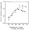
Un exemple de réalisation de l'invention sera maintenant décrit en détail en relation avec la figure unique jointe qui représente la variation du taux de conversion d'énergie de piles solaires à silicium amorphe utilisant des couches conductrices d'oxyde d'étain selon l'invention d'une part, classiques d'autre part, en fonction de l'épaisseur de ces couches.An exemplary embodiment of the invention will now be described in detail in connection with the single attached figure which represents the variation of the energy conversion rate of amorphous silicon solar cells using conductive layers of tin oxide according to invention on the one hand, conventional on the other hand, depending on the thickness of these layers.
Des piles solaires ont été réalisées d'une part à partir de substrats conducteurs selon l'invention, d'autre part à partir de substrats classiques et des comparaisons de performances ont été faites.Solar cells were produced on the one hand from conductive substrates according to the invention, on the other hand from conventional substrates and performance comparisons were made.
Pour réaliser ces piles solaires, on procède comme suit :
- . on prépare des supports en verre sodo-calcique de 25 mm x 30 mm, de 1,1 mm d'épaisseur, on les lave, on les sèche et on les recouvre d'une couche de silice,
- . ensuite, on les revêt d'une couche transparente à base d'oxyde d'étain pour obtenir le substrat selon l'invention, par la méthode C.V.D., en envoyant sur eux, lorsqu'ils sont chauffés à environ 550°C, un gaz constitué de vapeur de monobutyl trichlorure d'étain (C₄H₉SnCl₃), de vapeur d'eau, d'oxygène et d'azote.
- . soda-lime glass supports 25 mm x 30 mm, 1.1 mm thick, are prepared, washed, dried and covered with a layer of silica,
- . then, they are coated with a transparent layer based on tin oxide to obtain the substrate according to the invention, by the CVD method, by sending on them, when they are heated to approximately 550 ° C., a gas consisting of monobutyl tin trichloride vapor (C₄H₉SnCl₃), water vapor, oxygen and nitrogen.
En faisant varier le temps de dépôt sur 7 supports en verre, on a obtenu 7 épaisseurs différentes de couche d'oxyde d'étain : 0.20 - 0.39 - 0.59 - 0.7 - 0.8 - 0.98 et 1.15 microns. Ces supports ainsi revêtus d'une couche selon l'invention sont appelés les substrats "A".By varying the deposition time on 7 glass supports, 7 different thicknesses of tin oxide layer were obtained: 0.20 - 0.39 - 0.59 - 0.7 - 0.8 - 0.98 and 1.15 microns. These supports thus coated with a layer according to the invention are called the substrates "A".
Pour faire des comparaisons, sur des supports en verre identiques, on dépose par C.V.D. des couches d'oxyde d'étain dopé au fluor en ajoutant au gaz utilisé pour réaliser les échantillons "A" un gaz fluoré : du 1.1-difluoroéthane.To make comparisons, on identical glass supports, deposit by C.V.D. layers of tin oxide doped with fluorine by adding to the gas used to make the samples "A" a fluorinated gas: 1.1-difluoroethane.
En faisant varier les temps de dépôt, on obtient 6 substrats "B" ayant les épaisseurs de couche d'étain dopé au fluor suivantes : 0.19 - 0.37 - 0.57 - 0.75 - 0.92 et 1.10 microns. Avec ces substrats "A" et "B" on fabrique des piles solaires au silicium amorphe en procédant comme suit :
- . on dépose sur la couche d'oxyde d'étain une première épaisseur de silicium, semi-conducteur de type p, dopé au bore (a-SiC:H) de 0.015 micron d'épaisseur environ,
- . on dépose ensuite une seconde épaisseur de silicium, de semi-conducteur intrinsèque (a-Si:H) de 0,5 micron environ,
- . puis une troisième épaisseur dopée au phosphore, semi-conductrice de type n, Si(µC-Si):H monocristalline de 0.05 micron environ. On utilise pour cela comme matière première un gaz de monosilane SiH₄ sous une pression d'environ 170 pa, distribué par un dispositif de décharge luminescente à haute fréquence de type à couplage capacitif,
- . ensuite on dépose les électrodes en aluminium (d'épaisseur environ 0.1 micron) par exemple par la méthode de vaporisation sous vide (vide de l'ordre de 10-⁴ pa). Au moment de la réalisation de ces électrodes en aluminium, on pose un cache ayant des trous de 2 mm de diamètre et on fabrique ainsi des piles solaires de 2 mm de diamètre.
- . a first thickness of silicon, p-type semiconductor, doped with boron (a-SiC: H) of about 0.015 micron in thickness, is deposited on the tin oxide layer,
- . a second thickness of silicon, of intrinsic semiconductor (a-Si: H) of approximately 0.5 micron is then deposited,
- . then a third phosphor doped thickness, n-type semiconductor, Si (µC-Si): H monocrystalline of about 0.05 micron. For this, a monosilane gas SiH₄ is used as a raw material under a pressure of approximately 170 pa, distributed by a high frequency luminescent discharge device of the capacitive coupling type,
- . then the aluminum electrodes (approximately 0.1 micron thick) are deposited, for example by the vacuum vaporization method (vacuum of the order of 10-⁴ pa). When these aluminum electrodes are produced, a cover is placed with holes 2 mm in diameter and solar cells with a diameter of 2 mm are thus produced.
En exposant les piles solaires ainsi obtenues à une lumière de 100 mW/cm² d'AM1, on mesure le taux de conversion d'énergie et on utilise ces résultats pour construire les courbes de la figure jointe.By exposing the solar cells thus obtained to a light of 100 mW / cm² of AM1, the energy conversion rate is measured and these results are used to construct the curves of the attached figure.
D'après cette figure, on remarque que lorsque l'épaisseur est supérieure à 0.7 micron, les piles fabriquées à partir des substrats "A" ont un meilleur taux de conversion de l'énergie que celles fabriquées à partir des substrats "B".According to this figure, it is noted that when the thickness is greater than 0.7 microns, the batteries produced from substrates "A" have a better energy conversion rate than those manufactured from substrates "B".
On peut admettre que la transmission lumineuse obtenue avec des couches à base d'oxyde d'étain résultant d'un composé contenant du chlore, mais absolument aucun autre halogène et en particulier pas de fluor, soit meilleure que pour des couches d'oxyde d'étain dopées au fluor. Même si la résistance électrique d'une telle couche non dopée est plus faible que celle d'une couche dopée au fluor, du fait de la meilleure transmission de la lumière visible, le taux de conversion photoélectrique est amélioré.It can be admitted that the light transmission obtained with layers based on tin oxide resulting from a compound containing chlorine, but absolutely no other halogen and in particular no fluorine, is better than for layers of oxide of doped with fluorine. Even if the electrical resistance of such an undoped layer is lower than that of a fluorine doped layer, due to the better transmission of visible light, the photoelectric conversion rate is improved.
En outre pour des épaisseurs un peu élevées de la couche d'oxyde d'étain, supérieures à celles de l'ordre de 0.5 micron classiquement employées, et en particulier supérieures à 0.7 micron, la résistance électrique est un peu abaissée, du fait de l'épaisseur d'une part, et du fait que la taille des cristaux formés est augmentée, ce qui modifie de façon favorable l'état de surface de la couche, d'autre part.In addition, for slightly higher thicknesses of the tin oxide layer, greater than those of the order of 0.5 micron conventionally used, and in particular greater than 0.7 micron, the electrical resistance is slightly lowered, due to the thickness on the one hand, and the fact that the size of the crystals formed is increased, which favorably modifies the surface condition of the layer, on the other hand.
Claims (8)
- Conductive, transparent substrate for a photoelectric element, particularly a solar cell, comprising a support, more particularly of glass, coated with a transparent, conductive layer based on tin dioxide obtained by thermal decomposition and oxidation, in contact with the support raised to a high temperature, of a compound of tin containing chlorine, but without any other halogen, characterized in that it has a thickness of at least 0.7 micron (µm).
- Conductive, transparent substrate for a photoelectric element, particularly a solar cell, comprising a support, more particularly of glass, coated with a transparent, conductive layer based on tin dioxide, characterized in that it is obtained by thermal decomposition and oxidation, in contact with the support raised to a high temperature, of a chlorine-free tin compound, which is associated with another compund containing chlorine, such as HCl and in that it has a thickness of at least 0.7 micron (µm).
- Substrate according to claims 1 or 2, characterized in that the tin dioxide layer with which it is covered has a thickness of 0.8 to 1.2 microns (µm).
- Substrate according to one of the claims 1 to 3, characterized in that the chlorine-containing tin compound is chosen from the group consisting of tin monobutyl trichloride, tin tetrachloride and tin dimethyl dichloride.
- Substrate according to either of the claims 2 and 3, characterized in that the completely halogen-free tin compound is chosen from the group consisting of:
(CH2n+1)₄ Sn with n = 1, 2, 3 or 4
(CH₃)₂ SnH₂, (C₄H₉)₃ SnH
(CH₄H₉)₂ Sn (COOCH₃)₂. - Substrate according to any one of the claims 1 to 5, characterized in that the conductive layer is formed on a silica layer initially formed on the support.
- Amorphous silicon solar cell, characterized in that it has a transparent, conductive substrate comprising a glass support coated with a tin dioxide-based layer obtained from a tin compound containing chlorine, with the exception of any other halogen, having a thickness of at least 0.7 micron (µm).
- Solar cell according to claim 7, characterized in that the substrate with the tin dioxide layer is covered with thicknesses of amorphous silicon and aluminium electrodes.
Priority Applications (1)
| Application Number | Priority Date | Filing Date | Title |
|---|---|---|---|
| AT86402059T ATE71925T1 (en) | 1985-09-20 | 1986-09-19 | CONDUCTIVE AND TRANSPARENT SUBSTRATE FOR A PHOTOELECTRIC ELEMENT. |
Applications Claiming Priority (2)
| Application Number | Priority Date | Filing Date | Title |
|---|---|---|---|
| JP60208363A JPS6269405A (en) | 1985-09-20 | 1985-09-20 | Transparent conductive substrate for photoelectric element |
| JP208363/85 | 1985-09-20 |
Publications (3)
| Publication Number | Publication Date |
|---|---|
| EP0216703A2 EP0216703A2 (en) | 1987-04-01 |
| EP0216703A3 EP0216703A3 (en) | 1989-04-26 |
| EP0216703B1 true EP0216703B1 (en) | 1992-01-22 |
Family
ID=16555049
Family Applications (1)
| Application Number | Title | Priority Date | Filing Date |
|---|---|---|---|
| EP86402059A Expired - Lifetime EP0216703B1 (en) | 1985-09-20 | 1986-09-19 | Conducting and transparent substrate for a photoelectric element |
Country Status (5)
| Country | Link |
|---|---|
| EP (1) | EP0216703B1 (en) |
| JP (1) | JPS6269405A (en) |
| AT (1) | ATE71925T1 (en) |
| DE (1) | DE3683575D1 (en) |
| ES (1) | ES2003352A6 (en) |
Families Citing this family (5)
| Publication number | Priority date | Publication date | Assignee | Title |
|---|---|---|---|---|
| JPH07112076B2 (en) * | 1987-05-07 | 1995-11-29 | 日本板硝子株式会社 | Transparent conductive film body having a two-layer structure |
| JP2853125B2 (en) * | 1988-03-17 | 1999-02-03 | 日本板硝子株式会社 | Method for producing transparent conductive film |
| DE19715048C2 (en) * | 1997-04-11 | 1999-08-19 | Bosch Gmbh Robert | Process for structuring a transparent, electrically conductive layer |
| US6602606B1 (en) * | 1999-05-18 | 2003-08-05 | Nippon Sheet Glass Co., Ltd. | Glass sheet with conductive film, method of manufacturing the same, and photoelectric conversion device using the same |
| CN104310790A (en) * | 2014-09-28 | 2015-01-28 | 中国建材国际工程集团有限公司 | Preparation method of large-area transparent conducting film glass |
Family Cites Families (3)
| Publication number | Priority date | Publication date | Assignee | Title |
|---|---|---|---|---|
| JPS5534668A (en) * | 1978-09-04 | 1980-03-11 | Toshiba Corp | Forming method for transparent conductive composite film |
| JPS59162269A (en) * | 1983-03-07 | 1984-09-13 | Nippon Sheet Glass Co Ltd | Method for forming tin oxide film on base body |
| JPS59136477A (en) * | 1982-12-23 | 1984-08-06 | Nippon Sheet Glass Co Ltd | Formation of tin oxide film on substrate |
-
1985
- 1985-09-20 JP JP60208363A patent/JPS6269405A/en active Granted
-
1986
- 1986-09-19 AT AT86402059T patent/ATE71925T1/en not_active IP Right Cessation
- 1986-09-19 DE DE8686402059T patent/DE3683575D1/en not_active Expired - Fee Related
- 1986-09-19 EP EP86402059A patent/EP0216703B1/en not_active Expired - Lifetime
- 1986-09-19 ES ES8602025A patent/ES2003352A6/en not_active Expired - Fee Related
Also Published As
| Publication number | Publication date |
|---|---|
| DE3683575D1 (en) | 1992-03-05 |
| EP0216703A2 (en) | 1987-04-01 |
| EP0216703A3 (en) | 1989-04-26 |
| ATE71925T1 (en) | 1992-02-15 |
| JPS6269405A (en) | 1987-03-30 |
| JPH0572686B2 (en) | 1993-10-12 |
| ES2003352A6 (en) | 1991-03-16 |
Similar Documents
| Publication | Publication Date | Title |
|---|---|---|
| US9059370B2 (en) | Zinc oxide film method and structure for CIGS cell | |
| EP1189288B1 (en) | Photoelectric conversion device | |
| CA1318193C (en) | Transparent electrical conductor fabrication | |
| AU2005200023B2 (en) | Photovoltaic device | |
| US20030005956A1 (en) | Photoelectric device | |
| CN111416013A (en) | Heterojunction solar cell with hydrogenated amorphous silicon oxynitride film as passivation layer | |
| Gau et al. | Preparation of amorphous silicon films by chemical vapor deposition from higher silanes SinH2n+ 2 (n≳ 1) | |
| EP0216703B1 (en) | Conducting and transparent substrate for a photoelectric element | |
| JPWO2005109526A1 (en) | Thin film photoelectric converter | |
| EP0335769A2 (en) | Electroconducting glass and method of making the same | |
| JP2009117463A (en) | Thin-film photoelectric conversion device | |
| EP0382632B1 (en) | Electroconductive transparent substrate with two metallic-oxide layers, used especially in optoelectronic devices | |
| US5278015A (en) | Amorphous silicon film, its production and photo semiconductor device utilizing such a film | |
| JP2003188400A (en) | Crystalline silicon carbide film and manufacturing method thereof, and solar cell | |
| EP0290345B1 (en) | Conductive layer for photovoltaic elements | |
| JP2002237610A (en) | Photoelectric converter and its manufacturing method | |
| JP4187328B2 (en) | Photovoltaic element manufacturing method | |
| US5152833A (en) | Amorphous silicon film, its production and photo semiconductor device utilizing such a film | |
| JP2006332711A (en) | Photoelectric conversion device | |
| EP2104145A1 (en) | Glass substrate coated with thin films and method of manufacturing same | |
| JP5160574B2 (en) | Photoelectric conversion device | |
| JPH0121634B2 (en) | ||
| Osborne et al. | Stable hydrogenated amorphous silicon films deposited from silane and dichlorosilane by radio frequency plasma chemical vapor deposition | |
| US5258207A (en) | Amorphous silicon film, its production and photo semiconductor device utilizing such a film | |
| JP2822358B2 (en) | Manufacturing method of thin film solar cell |
Legal Events
| Date | Code | Title | Description |
|---|---|---|---|
| PUAI | Public reference made under article 153(3) epc to a published international application that has entered the european phase |
Free format text: ORIGINAL CODE: 0009012 |
|
| AK | Designated contracting states |
Kind code of ref document: A2 Designated state(s): AT BE CH DE FR GB IT LI LU NL SE |
|
| PUAL | Search report despatched |
Free format text: ORIGINAL CODE: 0009013 |
|
| AK | Designated contracting states |
Kind code of ref document: A3 Designated state(s): AT BE CH DE FR GB IT LI LU NL SE |
|
| 17P | Request for examination filed |
Effective date: 19890920 |
|
| RAP1 | Party data changed (applicant data changed or rights of an application transferred) |
Owner name: SAINT-GOBAIN VITRAGE INTERNATIONAL |
|
| 17Q | First examination report despatched |
Effective date: 19900829 |
|
| GRAA | (expected) grant |
Free format text: ORIGINAL CODE: 0009210 |
|
| AK | Designated contracting states |
Kind code of ref document: B1 Designated state(s): AT BE CH DE FR GB IT LI LU NL SE |
|
| REF | Corresponds to: |
Ref document number: 71925 Country of ref document: AT Date of ref document: 19920215 Kind code of ref document: T |
|
| REF | Corresponds to: |
Ref document number: 3683575 Country of ref document: DE Date of ref document: 19920305 |
|
| ITF | It: translation for a ep patent filed | ||
| GBT | Gb: translation of ep patent filed (gb section 77(6)(a)/1977) | ||
| PLBE | No opposition filed within time limit |
Free format text: ORIGINAL CODE: 0009261 |
|
| STAA | Information on the status of an ep patent application or granted ep patent |
Free format text: STATUS: NO OPPOSITION FILED WITHIN TIME LIMIT |
|
| 26N | No opposition filed | ||
| EPTA | Lu: last paid annual fee | ||
| EAL | Se: european patent in force in sweden |
Ref document number: 86402059.9 |
|
| PGFP | Annual fee paid to national office [announced via postgrant information from national office to epo] |
Ref country code: SE Payment date: 19980810 Year of fee payment: 13 |
|
| PGFP | Annual fee paid to national office [announced via postgrant information from national office to epo] |
Ref country code: GB Payment date: 19980825 Year of fee payment: 13 |
|
| PGFP | Annual fee paid to national office [announced via postgrant information from national office to epo] |
Ref country code: AT Payment date: 19980909 Year of fee payment: 13 |
|
| PGFP | Annual fee paid to national office [announced via postgrant information from national office to epo] |
Ref country code: FR Payment date: 19980910 Year of fee payment: 13 |
|
| PGFP | Annual fee paid to national office [announced via postgrant information from national office to epo] |
Ref country code: BE Payment date: 19980915 Year of fee payment: 13 |
|
| PGFP | Annual fee paid to national office [announced via postgrant information from national office to epo] |
Ref country code: NL Payment date: 19980930 Year of fee payment: 13 |
|
| PGFP | Annual fee paid to national office [announced via postgrant information from national office to epo] |
Ref country code: DE Payment date: 19981010 Year of fee payment: 13 |
|
| PGFP | Annual fee paid to national office [announced via postgrant information from national office to epo] |
Ref country code: LU Payment date: 19981023 Year of fee payment: 13 |
|
| PGFP | Annual fee paid to national office [announced via postgrant information from national office to epo] |
Ref country code: CH Payment date: 19981221 Year of fee payment: 13 |
|
| PG25 | Lapsed in a contracting state [announced via postgrant information from national office to epo] |
Ref country code: LU Free format text: LAPSE BECAUSE OF NON-PAYMENT OF DUE FEES Effective date: 19990919 Ref country code: GB Free format text: LAPSE BECAUSE OF NON-PAYMENT OF DUE FEES Effective date: 19990919 Ref country code: AT Free format text: LAPSE BECAUSE OF NON-PAYMENT OF DUE FEES Effective date: 19990919 |
|
| PG25 | Lapsed in a contracting state [announced via postgrant information from national office to epo] |
Ref country code: SE Free format text: THE PATENT HAS BEEN ANNULLED BY A DECISION OF A NATIONAL AUTHORITY Effective date: 19990929 |
|
| PG25 | Lapsed in a contracting state [announced via postgrant information from national office to epo] |
Ref country code: LI Free format text: LAPSE BECAUSE OF NON-PAYMENT OF DUE FEES Effective date: 19990930 Ref country code: CH Free format text: LAPSE BECAUSE OF NON-PAYMENT OF DUE FEES Effective date: 19990930 Ref country code: BE Free format text: LAPSE BECAUSE OF NON-PAYMENT OF DUE FEES Effective date: 19990930 |
|
| BERE | Be: lapsed |
Owner name: SAINT-GOBAIN VITRAGE INTERNATIONAL Effective date: 19990930 |
|
| PG25 | Lapsed in a contracting state [announced via postgrant information from national office to epo] |
Ref country code: NL Free format text: LAPSE BECAUSE OF NON-PAYMENT OF DUE FEES Effective date: 20000401 |
|
| GBPC | Gb: european patent ceased through non-payment of renewal fee |
Effective date: 19990919 |
|
| EUG | Se: european patent has lapsed |
Ref document number: 86402059.9 |
|
| REG | Reference to a national code |
Ref country code: CH Ref legal event code: PL |
|
| PG25 | Lapsed in a contracting state [announced via postgrant information from national office to epo] |
Ref country code: FR Free format text: LAPSE BECAUSE OF NON-PAYMENT OF DUE FEES Effective date: 20000531 |
|
| NLV4 | Nl: lapsed or anulled due to non-payment of the annual fee |
Effective date: 20000401 |
|
| PG25 | Lapsed in a contracting state [announced via postgrant information from national office to epo] |
Ref country code: DE Free format text: LAPSE BECAUSE OF NON-PAYMENT OF DUE FEES Effective date: 20000701 |
|
| REG | Reference to a national code |
Ref country code: FR Ref legal event code: ST |
|
| PG25 | Lapsed in a contracting state [announced via postgrant information from national office to epo] |
Ref country code: IT Free format text: LAPSE BECAUSE OF NON-PAYMENT OF DUE FEES Effective date: 20050919 |