EP0211385B1 - Speicheranordnung - Google Patents
Speicheranordnung Download PDFInfo
- Publication number
- EP0211385B1 EP0211385B1 EP86110494A EP86110494A EP0211385B1 EP 0211385 B1 EP0211385 B1 EP 0211385B1 EP 86110494 A EP86110494 A EP 86110494A EP 86110494 A EP86110494 A EP 86110494A EP 0211385 B1 EP0211385 B1 EP 0211385B1
- Authority
- EP
- European Patent Office
- Prior art keywords
- memory device
- memory
- input
- data
- output
- Prior art date
- Legal status (The legal status is an assumption and is not a legal conclusion. Google has not performed a legal analysis and makes no representation as to the accuracy of the status listed.)
- Expired - Lifetime
Links
Images


Classifications
-
- G—PHYSICS
- G06—COMPUTING OR CALCULATING; COUNTING
- G06F—ELECTRIC DIGITAL DATA PROCESSING
- G06F7/00—Methods or arrangements for processing data by operating upon the order or content of the data handled
- G06F7/76—Arrangements for rearranging, permuting or selecting data according to predetermined rules, independently of the content of the data
- G06F7/78—Arrangements for rearranging, permuting or selecting data according to predetermined rules, independently of the content of the data for changing the order of data flow, e.g. matrix transposition or LIFO buffers; Overflow or underflow handling therefor
- G06F7/785—Arrangements for rearranging, permuting or selecting data according to predetermined rules, independently of the content of the data for changing the order of data flow, e.g. matrix transposition or LIFO buffers; Overflow or underflow handling therefor having a sequence of storage locations each being individually accessible for both enqueue and dequeue operations, e.g. using a RAM
-
- G—PHYSICS
- G06—COMPUTING OR CALCULATING; COUNTING
- G06F—ELECTRIC DIGITAL DATA PROCESSING
- G06F5/00—Methods or arrangements for data conversion without changing the order or content of the data handled
- G06F5/06—Methods or arrangements for data conversion without changing the order or content of the data handled for changing the speed of data flow, i.e. speed regularising or timing, e.g. delay lines, FIFO buffers; over- or underrun control therefor
- G06F5/16—Multiplexed systems, i.e. using two or more similar devices which are alternately accessed for enqueue and dequeue operations, e.g. ping-pong buffers
-
- G—PHYSICS
- G11—INFORMATION STORAGE
- G11C—STATIC STORES
- G11C8/00—Arrangements for selecting an address in a digital store
- G11C8/04—Arrangements for selecting an address in a digital store using a sequential addressing device, e.g. shift register, counter
Definitions
- the present invention relates to a memory device, and more particularly to a memory device basically identical to that of a shift register having a variable depth of stages.
- Shift registers comprising a plurality of registers cascade-connected to shift their contents in sequence play an important role in computational processings or image processings, etc. Products having various capacities of 4,8,16, 1024 and 64K bits, etc. have been available.
- US-A-4 395 764 shows a device having addressing means, cyclically changing, and two memory blocks, all arranged to read and write data in one clock cycle as a shift register of variable depth.
- WO 85/02935 shows a RAM device arranged as a shift register having a counter supplying addresses.
- This shift register 10 comprises eight stages of flip-flops 1 to 8 wherein Q outputs of the flip-flops are respectively connected to D inputs of the next stages thereof and a clock line is commonly connected to the respective flip-flops.
- All object of the present invention is to provide a memory device having an arbitrary number of stages.
- Another object of the present invention is to provide a memory device having an arbitrary number of stages and capable of outputting the same value every single-cyclic clock signal.
- a further object of the present invention is to provide a memory device having an arbitrary number of stages and capable of changing memory contents according to need.
- a still further object of the present invention is to provide a memory device having an arbitrary depth of 2N stages using a double-cyclic N clock signal.
- a memory device comprising:
- a basic concept of a memory device there is shown, in a block form, a basic concept of a memory device.
- the memory device shown is configured so that addresses of a memory means 20 for storing input data therein are designated by an addressing means 30, thus effecting write and read operations of data.
- This addressing means 30 has a function to cyclically designate addresses of the memory means 20 so that the same value of the address is not designated during one cycle. For instance, when the number of the designation is equal to N, the addressing means 30 functions as an mod-N counter (defined as a counter having N states in the positional notation) which is decremented by one from N-1 per each clock pulse to return to the value of N-1 for a second time when the count value is equal to zero.
- the memory means 20 has a function to store data into a memory area assigned to an address designated by the addressing means 30 and/or read the data therefrom.
- dynamic RAM of 64K bit configuration may be used.
- the memory device thus configured operates as follows. First, an address is designated by using the addressing means 30 to store data into a memory area assigned to the designated address. In the next step, by allowing the addressing means 30 to circulate so as to designate the same address in the same order, data is read from the concerned memory area, thus making it possible to fetch the same data previously stored therefrom.
- the memory device functions as a shift register.
- Fig. 3 is a circuit diagram base on the configuration shown in Fig. 2.
- This memory device comprises a RAM 40, a counter 50 for designating write and read addresses of the RAM 40 one by one per each clock pulse, a shift register 60 for setting a count value to the counter, a control circuit 70 for effecting control of the entirety of the memory circuit, and a selector 80.
- the RAM 40 is comprised of a dynamic RAM of 64K bit configuration.
- the RAM 40 is provided with 16 address lines, thus making it possible to write data into a memory area assigned to an address determined by the selection of the address lines or read it from the memory area assigned to the address.
- the RAM 40 is provided with a write enable (WE) terminal, a data input (Din) terminal and a data output (D out ) terminal.
- WE write enable
- Din data input
- D out data output
- the counter 50 counts down one by one per each clock pulse from a designated value less than (2 16- 1). After the count value reaches zero, the counter 50 repeatedly counts down from the value of n. In this counter 50, the value of n is determined by 16 set inputs.
- the shift register 60 is configured as a sixteen stage shift register for setting the value of n wherein outputs of their stages are set inputs of the counter, respectively.
- the control circuit 70 is comprised of an AND gate to which a clock (CLK) signal and shift enable (SFTE) signal are input. An output of the control circuit 70 is input to a CLK terminal of the shift register 60, a CLK terminal of the counter 50 and a WE (write enable) terminal of the RAM 40.
- CLK clock
- SFTE shift enable
- the selector 80 comprises an AND gate 81 to which a D out output of the RAM 40 and a signal obtained by inverting an initialization (INIT) signal using an inverter 84 are input, an AND gate 82 to which the INIT signal and an output of the shift register 60 are input, and an OR gate to which outputs from the two AND gates are input.
- An output of the OR gate 83 is output as an output of the entire circuit.
- the INIT signal is also input to a LOAD terminal of the counter 50.
- Fig. 4 is circuit diagram illustrating an embodiment obtained by improving the configuration shown in Fig. 2.
- the memory device comprises two memory means 20a and 20b subject to addressing by a common addressing means represented by the same reference numeral 30 as in the circuit shown in Fig. 2.
- the memory device further comprises a flip-flop 31 which inverts its state when a designated value becomes zero in response to the completion of a single-cyclic clock signal.
- An output signal of the flip-flop 31 is delivered to a write enable (WE) terminal of the memory means 20a through an inverter 35 and is directly delivered to a write enable (WE) terminal of the memory means 20b so that signals delivered to the WE terminals of the memory means 20a and 20b are opposite to each other in their logical states.
- WE write enable
- An output of the memory means 20a and an inverted signal of the output signal from the flip-flop 31 are input to an AND gate 32.
- An output of the memory means 20b and the output signal from the flip-flop 31 are input to an AND gate 33.
- Two outputs of the AND gates 32 and 33 are input to an OR gate 34.
- the memory means 20b is in write-disabled state and the memory means 20a is in write enabled state.
- the memory means 20b is in write-disabled state and the memory means 20a is in write enabled state.
- the addressing means 30 data is read from the memory means 20b one by one per each clock pulse and the data thus read is output through the AND gate 33 and the OR gate 34.
- data is written into a memory area assigned to a designated address of the memory means 20a.
- the output of the memory means 20a is disallowed because the AND gate 32 is in disable state.
- This embodiment can eliminate the possibility of discontinuity of data which would occur in the embodiment shown in Fig. 2 and realize substantially the same memory device as a 2N state shift register.
- a further memory device wherein memory means represented by reference numeral 20' and the addressing means 30 are provided in the same manner as in the configuration shown in Fig. 2.
- the addressing means 30 is basically identical to that in the configuration shown in Fig. 2, but the memory means 20' differs from that in the latter in that it has a function to write data while reading it, i.e., effect so-called read modify write operation.
- An output of the memory means 20' is fetched therefrom and at the same time the output is fed back to the input side of the memory means 20' to again input the output thus fed back to the memory means through a switch means 21.
- the switch means 21 may be comprised of e.g. a gate circuit for selecting a new data input or a re-input of memory contents.
- the memory device thus configured, by allowing the addressing means 30 to cyclically designate the same value in the same order during each cycle and by setting the switch means 21 so as to rewrite an output of the memory means 20', it is possible to repeatedly fetch a series of the same data per each cycle. Further, by changing the number of addresses assigned to memory areas in the memory means 20' designated by the addressing means 30, the memory device in this embodiment can function as a shift register having an arbitrary number of stages. In addition, when the switch means 21 is set to the DATA input, the memory device in this embodiment has substantially the same configuration and operation as in the device shown in Fig. 1.
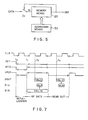
- Fig. 6 is a circuit diagram illustrating the detail of the configuration shown in Fig. 5.
- This memory device shown is provided, as the same circuit components as those in the circuit shown in Fig. 3, with the RAM 40, the counter 50 for designating write and read addresses of the RAM 40 one by one per each clock pulse, the shift register 60 for setting a count value to the counter 50, the control circuit 70 for effecting the entirety of the circuit, and the selector 80, and it is provided with a selector 90 newly added.
- the selector 90 comprises an AND gate 92 to which an update (UPDT) signal and an entire circuit input D in areinput, an AND gate 91 to which a signal obtained by inverting the UPDT signal using an inverter 90 and an output of the selector 80 are input, and an OR gate 93 to which outputs from the two AND gates are input.
- An output of the OR gate 93 is input to an input D in of the RAM 40 and a D terminal of the shift register 60.
- the UPDT signal is set at H level to input store data into the shift register 60, i.e. data indicative of a count start number n.
- a SFTE signal of H level is input to the control circuit 60 to input 16 clock pulses so that the data indicative of the count start number is stored into the shift register 60.
- the counter start number n is stored into the shift register 60 in a binary form. Accordingly, when an INIT signal of H level is input to the LOAD terminal of the counter 50, the count start number n is set to the counter 50. Then, when the INIT signal shifts to L level, the data indicative of the count start number n is maintained in the counter 50 as it is. The initialization is thus completed. Accordingly, when the INIT signal and the SFTE signal are respectively set at L level at time to, the initialized condition is maintained.
- this memory device operates so as to output SFTE signal of H level from the control unit 70 and to output UPDT signal of H level from the selector 90 (time ti in Fig. 7).
- the DIN input becomes valid because an output of the AND gate 92 shifts to H level.
- the RAM 40 effects the read modify write operation as previously described. Accordingly, the data read output D out becomes valid at the time of a falling of the CLK signal at time t 2 in Fig. 7, with the result that the write input D in becomes valid within a portion of the valid period of the data read output.
- this N bit data is delivered to the D in input terminal of the RAM 40 via the AND gate 92 and the OR gate 93.
- the CLK signal is input from the control circuit 70 to the CLK terminal of the counter 50 and the WE terminal of the RAM 40. Accordingly, data is written, bit by bit, into memory areas assigned to respective addresses of the RAM 40 corresponding to count values output from the counter 50.
- the count value of the counter 50 is equal to zero, the count value represents n for a second time at timing of the next clock pulse.
- the contents stored in the RAM 40 are output as the data read output D ou; irrespective of the fact that any data is input as the DIN. Namely, for a time period during which a count value of the counter 50 circulates, data is fetched in order of storing data in the previous cycle.
- the UPDT signal and the SFTE signal are set at H level to input valid data from the DIN terminal to store it into the RAM 40.
- the UPDT signal is set at L level.
- an input to the AND gate 91 shifts to H level.
- the DOUT signal is input to the D in terminal. Accordingly, since the D in input becomes valid for a time period during which the DOUT output is valid as indicated by time t 3 in Fig. 7, it is possible to store the memory content of the RAM 40 into the RAM 40 for a second time. Thus, the same memory contents can be repeatedly fetched.
- This memory device can be configured as e.g. a single-in- line package provided with lead wires for the above-mentioned terminals.
- this memory device has a circuit configuration such that a simple circuit e.g. a counter is only added to RAM. As a result, there is no possibility that an area for circuit components is increased, thus facilitating realization of integrated circuit.
- the counter which successively counts down one by one per each clock pulse is used for the addressing means.
- a counter to successively count up one by one or a counter which does not necessarily output continuous values, but outputs discrete different values during each cycle.
- the essential requirement for the addressing means is to have a function as state transition means capable of designating non-used write or read addresses of memory means without repeatedly addressing the same value during each cycle.
- a random number generator which does not generate the same number may be used. When such a random number generator is employed, it is required to reconstruct read data on the basis of designated addresses.
- the shift register is used to set the number of stages required for the counter operation to the counter. According to use, there are instances where there is no need to change the depth as the memory device. In these instances, the number of stages required for the counter operation may be set by ROM.
- the shift register employed in the above-mentioned embodiment is of the serial setting type, but shift registers of the parallel setting type may be used.
- the counter has the same operation mode at the time of writing of data as that at the time of reading of data. Accordingly, each memory device including such a counter functions as a FIFO memory. In addition to this, if addressing at the time of reading is carried out in order opposite to that at the time of writing, each memory device can be used as a FILO memory. For this purpose, a reversible shift register may be used for the shift register.
- the memory device is provided with memory means capable of storing data into a memory area assigned to an address designated or reading it therefrom, and addressing means for designating address values different from each other during each cycle. Accordingly, by selecting the number of address values designated by the addressing means, it is possible to provide a memory device having an arbitrary number of stages which has a capacity less than that of the memory means.
- the memory means capable of effecting read and write operations at the same time to deliver its output back to the input side thereof for a second time, it is possible to provide a memory device having an arbitrary number of stages which is capable of repeatedly outputting the same data.
Landscapes
- Engineering & Computer Science (AREA)
- Theoretical Computer Science (AREA)
- Physics & Mathematics (AREA)
- General Engineering & Computer Science (AREA)
- General Physics & Mathematics (AREA)
- Mathematical Physics (AREA)
- Microelectronics & Electronic Packaging (AREA)
- Dram (AREA)
- Shift Register Type Memory (AREA)
Claims (9)
dadurch gekennzeichnet, daß:
Priority Applications (1)
| Application Number | Priority Date | Filing Date | Title |
|---|---|---|---|
| EP91114289A EP0463640B1 (de) | 1985-07-30 | 1986-07-30 | Speicheranordnung zur Simulation eines Schieberegisters |
Applications Claiming Priority (2)
| Application Number | Priority Date | Filing Date | Title |
|---|---|---|---|
| JP60168027A JPS6228993A (ja) | 1985-07-30 | 1985-07-30 | 記憶装置 |
| JP168027/85 | 1985-07-30 |
Related Child Applications (1)
| Application Number | Title | Priority Date | Filing Date |
|---|---|---|---|
| EP91114289.1 Division-Into | 1986-07-30 |
Publications (3)
| Publication Number | Publication Date |
|---|---|
| EP0211385A2 EP0211385A2 (de) | 1987-02-25 |
| EP0211385A3 EP0211385A3 (en) | 1990-01-24 |
| EP0211385B1 true EP0211385B1 (de) | 1993-03-17 |
Family
ID=15860457
Family Applications (2)
| Application Number | Title | Priority Date | Filing Date |
|---|---|---|---|
| EP91114289A Expired - Lifetime EP0463640B1 (de) | 1985-07-30 | 1986-07-30 | Speicheranordnung zur Simulation eines Schieberegisters |
| EP86110494A Expired - Lifetime EP0211385B1 (de) | 1985-07-30 | 1986-07-30 | Speicheranordnung |
Family Applications Before (1)
| Application Number | Title | Priority Date | Filing Date |
|---|---|---|---|
| EP91114289A Expired - Lifetime EP0463640B1 (de) | 1985-07-30 | 1986-07-30 | Speicheranordnung zur Simulation eines Schieberegisters |
Country Status (3)
| Country | Link |
|---|---|
| EP (2) | EP0463640B1 (de) |
| JP (1) | JPS6228993A (de) |
| DE (2) | DE3688024T2 (de) |
Families Citing this family (11)
| Publication number | Priority date | Publication date | Assignee | Title |
|---|---|---|---|---|
| JPS63226777A (ja) * | 1987-03-16 | 1988-09-21 | Oki Electric Ind Co Ltd | 画像デ−タ読取方式 |
| US4899307A (en) * | 1987-04-10 | 1990-02-06 | Tandem Computers Incorporated | Stack with unary encoded stack pointer |
| NL8702672A (nl) * | 1987-11-09 | 1989-06-01 | Philips Nv | Serieel geheugen, alsmede beeldgeheugeninrichting en weergeeftoestel voorzien van een of meer seriele geheugens. |
| JPH0546808A (ja) * | 1991-08-12 | 1993-02-26 | Hitachi Electron Eng Co Ltd | Ocrの画像信号処理回路 |
| KR950011967B1 (ko) * | 1992-07-31 | 1995-10-12 | 임홍식 | 반도체 녹음기용 메모리 정리 장치 |
| FR2699707B1 (fr) * | 1992-12-23 | 1995-01-27 | Bull Sa | Système informatique à haut débit, composant de mémoire et contrôleur de mémoire en résultant. |
| US5526316A (en) * | 1994-04-29 | 1996-06-11 | Winbond Electronics Corp. | Serial access memory device |
| CA2287034A1 (en) * | 1998-12-03 | 2000-06-03 | Lucent Technologies, Inc. | A memory operated in a modified ping-pong mode |
| EP1073225B1 (de) * | 1999-01-12 | 2007-08-01 | Sony Corporation | System zur verteilung von informationen |
| US6874043B2 (en) | 2000-10-17 | 2005-03-29 | Bridgeworks Ltd. | Data buffer |
| GB0025495D0 (en) * | 2000-10-17 | 2000-11-29 | Digital Interfaces Ltd | A data buffer |
Citations (1)
| Publication number | Priority date | Publication date | Assignee | Title |
|---|---|---|---|---|
| WO1985002935A1 (en) * | 1983-12-23 | 1985-07-04 | Advanced Micro Devices, Inc. | Semiconductor memory device for serial scan applications |
Family Cites Families (6)
| Publication number | Priority date | Publication date | Assignee | Title |
|---|---|---|---|---|
| JPS5810299B2 (ja) * | 1977-10-26 | 1983-02-25 | 積水化成品工業株式会社 | 発泡シ−ト製の容器 |
| JPS5671105A (en) * | 1979-11-13 | 1981-06-13 | Yaskawa Electric Mfg Co Ltd | Shift register type programmable controller with memory |
| JPS5694589A (en) * | 1979-12-27 | 1981-07-31 | Nec Corp | Memory device |
| JPS57147183A (en) * | 1981-03-05 | 1982-09-10 | Fujitsu Ltd | Shift register |
| US4509142A (en) * | 1982-12-15 | 1985-04-02 | Texas Instruments Incorporated | Semiconductor memory device with pipeline access |
| FR2561429B1 (fr) * | 1984-03-13 | 1986-09-19 | Trt Telecom Radio Electr | Dispositif d'adressage pour fournir a une memoire des codes d'adresse |
-
1985
- 1985-07-30 JP JP60168027A patent/JPS6228993A/ja active Pending
-
1986
- 1986-07-30 DE DE19863688024 patent/DE3688024T2/de not_active Expired - Fee Related
- 1986-07-30 DE DE19863650508 patent/DE3650508T2/de not_active Expired - Fee Related
- 1986-07-30 EP EP91114289A patent/EP0463640B1/de not_active Expired - Lifetime
- 1986-07-30 EP EP86110494A patent/EP0211385B1/de not_active Expired - Lifetime
Patent Citations (1)
| Publication number | Priority date | Publication date | Assignee | Title |
|---|---|---|---|---|
| WO1985002935A1 (en) * | 1983-12-23 | 1985-07-04 | Advanced Micro Devices, Inc. | Semiconductor memory device for serial scan applications |
Also Published As
| Publication number | Publication date |
|---|---|
| DE3688024T2 (de) | 1993-09-09 |
| EP0463640A3 (en) | 1992-08-05 |
| JPS6228993A (ja) | 1987-02-06 |
| EP0463640B1 (de) | 1996-04-03 |
| DE3688024D1 (de) | 1993-04-22 |
| EP0211385A3 (en) | 1990-01-24 |
| EP0463640A2 (de) | 1992-01-02 |
| EP0211385A2 (de) | 1987-02-25 |
| DE3650508T2 (de) | 1996-09-12 |
| DE3650508D1 (de) | 1996-05-09 |
Similar Documents
| Publication | Publication Date | Title |
|---|---|---|
| EP0211385B1 (de) | Speicheranordnung | |
| US4599613A (en) | Display drive without initial disturbed state of display | |
| US5206834A (en) | Semiconductor memory device performing last in-first out operation and the method for controlling the same | |
| US5270981A (en) | Field memory device functioning as a variable stage shift register with gated feedback from its output to its input | |
| US5151954A (en) | Device capable of modifying a character according to a selected attribute code | |
| EP0057096A2 (de) | Informationsverarbeitungsanlage | |
| CA2022586A1 (en) | Scan converter control circuit having memories and address generator for generating zigzag address signal supplied to the memories | |
| US5572198A (en) | Method and apparatus for routing in reduced switch matrices to provide one hundred percent coverage | |
| JPS59112334A (ja) | シ−ケンス発生器 | |
| US5130923A (en) | Selective dynamic RAM address generator with provision for automatic refresh | |
| KR910009296B1 (ko) | 순차접근 기억장치 | |
| US5633656A (en) | Controlling apparatus for display of an on-screen menu in a display device | |
| JPS6297200A (ja) | 制御メモリ | |
| JPH0411388Y2 (de) | ||
| KR940003630B1 (ko) | 브이지에이의 다중폰트 선택회로 | |
| JPS5939053B2 (ja) | 記憶要素指定方式 | |
| JPH06232737A (ja) | N進カウンタ | |
| JPH0599986A (ja) | デジタル・パターン発生装置 | |
| JPS6237464B2 (de) | ||
| JPH0990936A (ja) | ディスプレイ表示装置 | |
| JPS63235985A (ja) | 文字パタ−ン発生装置 | |
| JPS62154176A (ja) | 表示デ−タ読出し制御方式 | |
| JPH02280527A (ja) | カウンタ回路 | |
| JPS61140992A (ja) | 表示制御方式 | |
| JPH03114098A (ja) | キャラクタジェネレータ |
Legal Events
| Date | Code | Title | Description |
|---|---|---|---|
| PUAI | Public reference made under article 153(3) epc to a published international application that has entered the european phase |
Free format text: ORIGINAL CODE: 0009012 |
|
| 17P | Request for examination filed |
Effective date: 19860730 |
|
| AK | Designated contracting states |
Kind code of ref document: A2 Designated state(s): DE FR GB |
|
| PUAL | Search report despatched |
Free format text: ORIGINAL CODE: 0009013 |
|
| AK | Designated contracting states |
Kind code of ref document: A3 Designated state(s): DE FR GB |
|
| 17Q | First examination report despatched |
Effective date: 19910214 |
|
| GRAA | (expected) grant |
Free format text: ORIGINAL CODE: 0009210 |
|
| XX | Miscellaneous (additional remarks) |
Free format text: VERBUNDEN MIT 89113505.5/0410013 (EUROPAEISCHE ANMELDENUMMER/VEROEFFENTLICHUNGSNUMMER) DURCH ENTSCHEIDUNG VOM 12.01.93. |
|
| AK | Designated contracting states |
Kind code of ref document: B1 Designated state(s): DE FR GB |
|
| REF | Corresponds to: |
Ref document number: 3688024 Country of ref document: DE Date of ref document: 19930422 |
|
| ET | Fr: translation filed | ||
| PLBE | No opposition filed within time limit |
Free format text: ORIGINAL CODE: 0009261 |
|
| STAA | Information on the status of an ep patent application or granted ep patent |
Free format text: STATUS: NO OPPOSITION FILED WITHIN TIME LIMIT |
|
| 26N | No opposition filed | ||
| PGFP | Annual fee paid to national office [announced via postgrant information from national office to epo] |
Ref country code: GB Payment date: 19970721 Year of fee payment: 12 |
|
| PGFP | Annual fee paid to national office [announced via postgrant information from national office to epo] |
Ref country code: DE Payment date: 19970811 Year of fee payment: 12 |
|
| PG25 | Lapsed in a contracting state [announced via postgrant information from national office to epo] |
Ref country code: GB Free format text: LAPSE BECAUSE OF NON-PAYMENT OF DUE FEES Effective date: 19980730 |
|
| GBPC | Gb: european patent ceased through non-payment of renewal fee |
Effective date: 19980730 |
|
| REG | Reference to a national code |
Ref country code: FR Ref legal event code: D6 |
|
| PG25 | Lapsed in a contracting state [announced via postgrant information from national office to epo] |
Ref country code: DE Free format text: LAPSE BECAUSE OF NON-PAYMENT OF DUE FEES Effective date: 19990501 |
|
| PGFP | Annual fee paid to national office [announced via postgrant information from national office to epo] |
Ref country code: FR Payment date: 20050708 Year of fee payment: 20 |