EP0200569A2 - Monolitisch integriertes Schaltungsbauelement - Google Patents
Monolitisch integriertes Schaltungsbauelement Download PDFInfo
- Publication number
- EP0200569A2 EP0200569A2 EP86303380A EP86303380A EP0200569A2 EP 0200569 A2 EP0200569 A2 EP 0200569A2 EP 86303380 A EP86303380 A EP 86303380A EP 86303380 A EP86303380 A EP 86303380A EP 0200569 A2 EP0200569 A2 EP 0200569A2
- Authority
- EP
- European Patent Office
- Prior art keywords
- control signals
- control
- data
- signals
- responsive
- Prior art date
- Legal status (The legal status is an assumption and is not a legal conclusion. Google has not performed a legal analysis and makes no representation as to the accuracy of the status listed.)
- Withdrawn
Links
Images

Classifications
-
- G—PHYSICS
- G06—COMPUTING OR CALCULATING; COUNTING
- G06F—ELECTRIC DIGITAL DATA PROCESSING
- G06F15/00—Digital computers in general; Data processing equipment in general
- G06F15/76—Architectures of general purpose stored program computers
- G06F15/80—Architectures of general purpose stored program computers comprising an array of processing units with common control, e.g. single instruction multiple data processors
- G06F15/8007—Architectures of general purpose stored program computers comprising an array of processing units with common control, e.g. single instruction multiple data processors single instruction multiple data [SIMD] multiprocessors
- G06F15/8015—One dimensional arrays, e.g. rings, linear arrays, buses
-
- G—PHYSICS
- G06—COMPUTING OR CALCULATING; COUNTING
- G06F—ELECTRIC DIGITAL DATA PROCESSING
- G06F15/00—Digital computers in general; Data processing equipment in general
- G06F15/76—Architectures of general purpose stored program computers
- G06F15/78—Architectures of general purpose stored program computers comprising a single central processing unit
- G06F15/7828—Architectures of general purpose stored program computers comprising a single central processing unit without memory
- G06F15/7832—Architectures of general purpose stored program computers comprising a single central processing unit without memory on one IC chip (single chip microprocessors)
-
- H—ELECTRICITY
- H04—ELECTRIC COMMUNICATION TECHNIQUE
- H04Q—SELECTING
- H04Q11/00—Selecting arrangements for multiplex systems
- H04Q11/04—Selecting arrangements for multiplex systems for time-division multiplexing
- H04Q11/0407—Selecting arrangements for multiplex systems for time-division multiplexing using a stored program control
Definitions
- This invention relates to electronic signal processing circuits for processing a plurality of signals concurrently, and more particularly, to a monolithic integrated circuit device having a single on-chip element controlling a plurality of on-chip signal processors.
- Time-division multiplexed (TDM) signals is a common concern in the telecommunication field.
- a number of coder-decoders (CODECs) such as eight, may be incorporated onto a single monolithic integrated circuit chip, so that a number of time-multiplexed communication signals may be processed simultaneously. In this way, an eight-fold increase in throughput speed will be achieved over the time it would take to process the signals strictly sequentially by a single CODEC.
- each CODEC is (i) identical with that performed by all the other CODECs, and (ii) data-independent, in the sense that the steps executed by each CODEC are straight-line code with no data-dependent decision steps.
- time-shared signal processors To avoid this duplication of control elements in multi-channel applications, and thereby reduce the area requirement for control elements from 35% to a much smaller percentage, the prior art has employed time-shared signal processors. However, such time-sharing requires operation of the processor at ever-increasing speeds, until a cherent upper limit is reached. Beyond this point, dual, quad, octuple processors are employed on a single chip to further increase throughput speed. But due to die area limitations. even this approach reaches an inherent upper limit. Furthermore, each processor has its own control element, thereby unnecessarily using valuable die area, and imposing excessive design requirements, especially in the area of computer-aided design (CAD).
- CAD computer-aided design
- the present invention concerns a single monolithic integrated circuit employing a multiple- intelligence, single-control (MISC) concept to save nearly 35% in die area with no compromise in throughput speed.
- MISC multiple- intelligence, single-control
- An alternative "systolic" embodiment using the MISC approach involves using a delay element in the control circuit connecting each processor to the central control element.
- the program executed by the control element would be run against the data in each TDM channel in a time-staggered manner.
- the time delay is chosen for each processor so that the program is run just as soon as the data in the time-division slot becomes available, thereby not having to wait to execute the program on the data in the first channel until the data in the last channel becomes available.
- a second alternative embodiment permits a certain amount of "customizing" of the control for each processor by appending a small individualized control element which influences only the processor to which it is directly connected.
- the bulk of the central control element need not be duplicated for each channel, only that small fraction which is designed expressly for the special needs of the channel.
- the 35% saving in die area would therefore be only slightly reduced in this variant while a corresponding flexibility is added.
- the instant MISC invention has possible application in the parallel processing of pixel information in digital graphics, in dual tone, multi-frequency (DTMF) detector and generator applications, in integrated service, digital network (ISDN) applications which involve software protocol processing cyclic redundancy code (CRC) generation and detection, and in the fast fourier transforms (FFT's) of a radar installation in which vast amounts of incoming data are sliced and processed within channels. And in a variety of multi-channel applications in which signal processing which would have heretofore been too costly is rendered available by the MISC invention.
- DTMF dual tone, multi-frequency
- ISDN integrated service, digital network
- FFT's fast fourier transforms
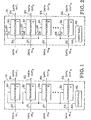
- FIG. 1 One embodiment of the multiple intelligence single control (MISC) architecture of the present invention is illustrated in block diagram form in Fig. 1. All elements shown in Fig. 1 could be incorporated onto a single monolithic integrated circuit chip 10. As shown in Fig. 1 a number of input data signals DATA_INt, DATA_IN2, DATA_IN3, ..., DATA_lNn, each of which could be analog or digital in nature, are conducted via respective input signal lines 20, 22, 24, ..., 26, to respective data-processors 30, 32, 34, ..., 36 contained within chip 10.
- DATA_INt DATA_IN2
- DATA_IN3 DATA_IN3
- DATA_lNn each of which could be analog or digital in nature
- a number of the data-processors could be connected to a single signal line in the case of time-division multiplexed (TDM) signals, or alternatively, a number of signal lines could be connected to a single data processor.
- TDM time-division multiplexed
- Each data-processor 30, 32, 34, ..., 36 is connected via signal line 40 to a control block 42, which is contained within chip 10.
- Control 42 may be, for example, a programmed logic array (PLA), capable of generating signals on line 40 which provide control signals for the data-processors 30, 32, 34, ..., 36.
- PLA programmed logic array
- the control and data-processing functions are separated in the architecture illustrated in Fig. 1, thereby avoiding the duplication of control elements, reducing the die area of the chip 10 and the number of interconnections, and improving reliability of chip 10.
- each signal line in Fig. 1 is shown as being single-conductor.
- Each data-processor 30, 32, 34, ..., 36 shown in Fig. 1 simultaneously executes the same series of operations which resuit from controi 42 executing a straight-line set of data-independent instructions and generating therefrom a series of control signals on line 40.
- Each data-processor 30, 32, 34,..., 36 receives the signals DATA_IN 1 , DATA_IN 2 , ..., DATA_INn on signal lines 20, 22, 24, ..., 26, respectively and generates therefrom signals DATA_OUT1, DATA_OUT 2 , DATA_OUT 3 , ..., DATA_OUTn on output signal lines 50, 52, 54, ..., 56, respectively, by performing the above-mentioned series of operations generated by control 42.
- a single data-processor may be connected to a number of output signal lines, or alternatively, a number of data-processors could be connected to a single output line in the case of TDM signals.
- FIG. 2 An alternative embodiment utilizing the MISC invention is illustrated in Fig. 2 in which a delay element is placed into the control path leading from control 42 to the data-processors 30, 32, 34, ..., 36.
- a delay element is placed into the control path leading from control 42 to the data-processors 30, 32, 34, ..., 36.
- FIG. 2 each data-processor 30, 32, 34, ..., 36 has a respective delay latch 60, 62, 64, ..., 66 included in the control path 40 from control 42.
- DATA_INn are derived from a time-division multiplexed (TDM) bit stream in which DATA_INi is in the ith time division, I ⁇ i ⁇ n, then a relatively long wait may be imposed before the nth time division arrives before simultaneous processing by all n data-processors can begin.
- TDM time-division multiplexed
- latch elements 60, 62, 64, ..., 66 provide progressively increasing control signal delay so that the DATA_INi input to data-processor i has been received before the control signals previously generated by control 42 are received and the data-processor performs the series of operations on the data from the ith time-division. In this "systolic" manner, no overall time penalty is imposed by the architecture shown in Fig. 2 while awaiting data to arrive.
- FIG. 3 A second arternative embodiment utilizing the MISC invention is illustrated in Fig. 3 in which the control 42 is augmented by a set of custom control elements 70, 72, 74...., 76, which perform a customized control operation for the respective data-processor 30, 32, 34, ..., 36.
- Each custom control receives a signal from control 42 via signal line 44 and generates therefrom individualized control signals to its respective data-processor 30, 32, 34, ..., 36 via signal lines 80, 82, 84, ..., 86, respectively. In this manner, the straight-fine set of data-independent instructions executed by the control 42 can be modified.
- the custom control 70, 72, 74, ..., 76 receive via respective signal lines 90, 92, 94, ..., 96, data-dependent signals generated by respective processors 30, 32, 34, ..., 36 which can cause the respective custom control to modify the customized straight-fine instructions executed by the control 42, so that a certain amount of data-dependency can be implemented by the MISC variation of Fig. 3.
Landscapes
- Engineering & Computer Science (AREA)
- Computer Hardware Design (AREA)
- Theoretical Computer Science (AREA)
- Physics & Mathematics (AREA)
- General Engineering & Computer Science (AREA)
- General Physics & Mathematics (AREA)
- Computing Systems (AREA)
- Microelectronics & Electronic Packaging (AREA)
- Computer Networks & Wireless Communication (AREA)
- Image Processing (AREA)
- Multi Processors (AREA)
- Communication Control (AREA)
- Time-Division Multiplex Systems (AREA)
Applications Claiming Priority (2)
| Application Number | Priority Date | Filing Date | Title |
|---|---|---|---|
| US73070885A | 1985-05-03 | 1985-05-03 | |
| US730708 | 1985-05-03 |
Publications (2)
| Publication Number | Publication Date |
|---|---|
| EP0200569A2 true EP0200569A2 (de) | 1986-11-05 |
| EP0200569A3 EP0200569A3 (de) | 1988-10-05 |
Family
ID=24936494
Family Applications (1)
| Application Number | Title | Priority Date | Filing Date |
|---|---|---|---|
| EP86303380A Withdrawn EP0200569A3 (de) | 1985-05-03 | 1986-05-02 | Monolitisch integriertes Schaltungsbauelement |
Country Status (2)
| Country | Link |
|---|---|
| EP (1) | EP0200569A3 (de) |
| JP (1) | JPS61264470A (de) |
Cited By (2)
| Publication number | Priority date | Publication date | Assignee | Title |
|---|---|---|---|---|
| EP0237013A3 (en) * | 1986-03-13 | 1989-02-08 | International Business Machines Corporation | Adaptive instruction processing by array processor having processor identification and data dependent status registers in each processing element |
| EP0636992A1 (de) * | 1993-07-14 | 1995-02-01 | Matsushita Electric Industrial Co., Ltd. | Pipeline-Rechner |
Family Cites Families (3)
| Publication number | Priority date | Publication date | Assignee | Title |
|---|---|---|---|---|
| US3980992A (en) * | 1974-11-26 | 1976-09-14 | Burroughs Corporation | Multi-microprocessing unit on a single semiconductor chip |
| DE3230054A1 (de) * | 1982-08-12 | 1984-02-16 | Siemens Ag | Demultiplexer |
| US4814973A (en) * | 1983-05-31 | 1989-03-21 | Hillis W Daniel | Parallel processor |
-
1986
- 1986-05-02 JP JP61102974A patent/JPS61264470A/ja active Pending
- 1986-05-02 EP EP86303380A patent/EP0200569A3/de not_active Withdrawn
Cited By (2)
| Publication number | Priority date | Publication date | Assignee | Title |
|---|---|---|---|---|
| EP0237013A3 (en) * | 1986-03-13 | 1989-02-08 | International Business Machines Corporation | Adaptive instruction processing by array processor having processor identification and data dependent status registers in each processing element |
| EP0636992A1 (de) * | 1993-07-14 | 1995-02-01 | Matsushita Electric Industrial Co., Ltd. | Pipeline-Rechner |
Also Published As
| Publication number | Publication date |
|---|---|
| JPS61264470A (ja) | 1986-11-22 |
| EP0200569A3 (de) | 1988-10-05 |
Similar Documents
| Publication | Publication Date | Title |
|---|---|---|
| US4385206A (en) | Programmable port sense and control signal preprocessor for a central office switching system | |
| EP0282267A3 (de) | Anpassungsfähige digitale Netzschnittstelle | |
| US4393381A (en) | Transfer bus matrix | |
| US5596578A (en) | Time division multiplexing data transfer system for digital audio data distribution | |
| CA1203876A (en) | Peripheral control for a digital telephone system | |
| EP0200569A2 (de) | Monolitisch integriertes Schaltungsbauelement | |
| US4317198A (en) | Rate converting bit stream demultiplexer and multiplexer | |
| US6330338B1 (en) | Process and device for mixing digital audio signals | |
| US4264984A (en) | High-speed multiplexing of keyboard data inputs | |
| EP0135383A2 (de) | Konferenzbrückenschaltungen | |
| JPS6297494A (ja) | バ−ストスイツチング通信システム用リンクスイツチ | |
| JPH04342010A (ja) | センサ制御器 | |
| SU679983A1 (ru) | Устройство приоритета | |
| AU627751B2 (en) | Multi-channel controller DO NOT SEAL CASE WITHDRAWN | |
| JP2634885B2 (ja) | 音声信号切替装置 | |
| JP2718090B2 (ja) | 高速回線アラーム情報通知方式 | |
| SU1190382A1 (ru) | Многоканальное устройство приоритетного обслуживани | |
| KR900007549Y1 (ko) | 디지탈 시리얼 데이타 전송시 속도 변환회로 | |
| JPH06188734A (ja) | 複数個の受け取られたアナログ信号を複数個の出力ディジタル信号に変換するための装置および変換の速度を増大させるためのシステム | |
| JPH04289776A (ja) | 複数インバータ間のデータ伝送方法 | |
| KR100197437B1 (ko) | 전전자 교환기의 프로세서와 디바이스간 통신 장치 | |
| JPH02138652A (ja) | アドレス設定方式 | |
| JPS61115159A (ja) | 信号列選択装置 | |
| JPH05225116A (ja) | パッケージ識別番号設定方式 | |
| JPS6035611B2 (ja) | 信号変換編集装置 |
Legal Events
| Date | Code | Title | Description |
|---|---|---|---|
| PUAI | Public reference made under article 153(3) epc to a published international application that has entered the european phase |
Free format text: ORIGINAL CODE: 0009012 |
|
| AK | Designated contracting states |
Kind code of ref document: A2 Designated state(s): AT BE CH DE FR GB IT LI LU NL SE |
|
| PUAL | Search report despatched |
Free format text: ORIGINAL CODE: 0009013 |
|
| AK | Designated contracting states |
Kind code of ref document: A3 Designated state(s): AT BE CH DE FR GB IT LI LU NL SE |
|
| 17P | Request for examination filed |
Effective date: 19881230 |
|
| 17Q | First examination report despatched |
Effective date: 19901016 |
|
| STAA | Information on the status of an ep patent application or granted ep patent |
Free format text: STATUS: THE APPLICATION IS DEEMED TO BE WITHDRAWN |
|
| 18D | Application deemed to be withdrawn |
Effective date: 19910227 |
|
| RIN1 | Information on inventor provided before grant (corrected) |
Inventor name: VENKATRAMAN, CHANDRASEKAR |