EP0195820B1 - Method of mounting electronic parts and an apparatus therefor - Google Patents
Method of mounting electronic parts and an apparatus therefor Download PDFInfo
- Publication number
- EP0195820B1 EP0195820B1 EP85904287A EP85904287A EP0195820B1 EP 0195820 B1 EP0195820 B1 EP 0195820B1 EP 85904287 A EP85904287 A EP 85904287A EP 85904287 A EP85904287 A EP 85904287A EP 0195820 B1 EP0195820 B1 EP 0195820B1
- Authority
- EP
- European Patent Office
- Prior art keywords
- circuit board
- distance
- holding device
- part holding
- mounting
- Prior art date
- Legal status (The legal status is an assumption and is not a legal conclusion. Google has not performed a legal analysis and makes no representation as to the accuracy of the status listed.)
- Expired - Lifetime
Links
- 238000000034 method Methods 0.000 title claims abstract description 13
- 238000010521 absorption reaction Methods 0.000 description 12
- 238000001514 detection method Methods 0.000 description 10
- 239000000758 substrate Substances 0.000 description 8
- 238000010586 diagram Methods 0.000 description 4
- 238000012423 maintenance Methods 0.000 description 4
- 230000006835 compression Effects 0.000 description 3
- 238000007906 compression Methods 0.000 description 3
- 230000004044 response Effects 0.000 description 3
- 239000006185 dispersion Substances 0.000 description 2
- 238000006073 displacement reaction Methods 0.000 description 2
- 238000005259 measurement Methods 0.000 description 2
- 230000003287 optical effect Effects 0.000 description 2
- 230000002159 abnormal effect Effects 0.000 description 1
- 230000003247 decreasing effect Effects 0.000 description 1
- 239000000428 dust Substances 0.000 description 1
- 230000000694 effects Effects 0.000 description 1
Images


Classifications
-
- H—ELECTRICITY
- H05—ELECTRIC TECHNIQUES NOT OTHERWISE PROVIDED FOR
- H05K—PRINTED CIRCUITS; CASINGS OR CONSTRUCTIONAL DETAILS OF ELECTRIC APPARATUS; MANUFACTURE OF ASSEMBLAGES OF ELECTRICAL COMPONENTS
- H05K13/00—Apparatus or processes specially adapted for manufacturing or adjusting assemblages of electric components
- H05K13/04—Mounting of components, e.g. of leadless components
-
- H—ELECTRICITY
- H05—ELECTRIC TECHNIQUES NOT OTHERWISE PROVIDED FOR
- H05K—PRINTED CIRCUITS; CASINGS OR CONSTRUCTIONAL DETAILS OF ELECTRIC APPARATUS; MANUFACTURE OF ASSEMBLAGES OF ELECTRICAL COMPONENTS
- H05K13/00—Apparatus or processes specially adapted for manufacturing or adjusting assemblages of electric components
- H05K13/08—Monitoring manufacture of assemblages
- H05K13/082—Integration of non-optical monitoring devices, i.e. using non-optical inspection means, e.g. electrical means, mechanical means or X-rays
-
- Y—GENERAL TAGGING OF NEW TECHNOLOGICAL DEVELOPMENTS; GENERAL TAGGING OF CROSS-SECTIONAL TECHNOLOGIES SPANNING OVER SEVERAL SECTIONS OF THE IPC; TECHNICAL SUBJECTS COVERED BY FORMER USPC CROSS-REFERENCE ART COLLECTIONS [XRACs] AND DIGESTS
- Y10—TECHNICAL SUBJECTS COVERED BY FORMER USPC
- Y10T—TECHNICAL SUBJECTS COVERED BY FORMER US CLASSIFICATION
- Y10T29/00—Metal working
- Y10T29/49—Method of mechanical manufacture
- Y10T29/49002—Electrical device making
- Y10T29/49117—Conductor or circuit manufacturing
- Y10T29/49124—On flat or curved insulated base, e.g., printed circuit, etc.
- Y10T29/4913—Assembling to base an electrical component, e.g., capacitor, etc.
-
- Y—GENERAL TAGGING OF NEW TECHNOLOGICAL DEVELOPMENTS; GENERAL TAGGING OF CROSS-SECTIONAL TECHNOLOGIES SPANNING OVER SEVERAL SECTIONS OF THE IPC; TECHNICAL SUBJECTS COVERED BY FORMER USPC CROSS-REFERENCE ART COLLECTIONS [XRACs] AND DIGESTS
- Y10—TECHNICAL SUBJECTS COVERED BY FORMER USPC
- Y10T—TECHNICAL SUBJECTS COVERED BY FORMER US CLASSIFICATION
- Y10T29/00—Metal working
- Y10T29/53—Means to assemble or disassemble
- Y10T29/53039—Means to assemble or disassemble with control means energized in response to activator stimulated by condition sensor
- Y10T29/53061—Responsive to work or work-related machine element
Definitions
- the present invention relates to a method and apparatus for mounting electronic parts, particularly electronic parts formed into a chip-like shape (which will be hereinafter referred to as chip part), on a circuit substrate such as printed circuit board; as e.g. known from GB-A-21 05 224.
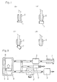
- Fig. 1(a) to Fig. 1(d) are illustrations of the conditions of vacuum absorption of the chip part 1.
- Fig. 1(a) through Fig. 1(d) respectively illustrate the condition that the chip part 1 has normally been absorbed by the nozzle 2, the condition that it has lengthwise been drawn thereby, the condition that it has obliquely been absorbed thereby, and the condition that it has not been attracted.
- Fig. 1(b) to Fig. 1(d) show error of the absorption of the chip part 1, and therefore detection should be made to determine these conditions.
- Fig. 2 is an illustration of a conventional vacuum system for the detection of absorption error of a chip part.
- the reference numerals 3 and 4 represent a filter, numeral 5 designating a throttle valve, numeral 6 depicting a magnet, numerals 7 and 8 being a proximity switch, and numeral 8 representing a vacuum source.
- This system is based on a method in which the absorption error is detected on view of differential pressure.
- the pressure of the nozzle side of a differential measuring device 10 is further decreased.
- the magnet 6 is moved in the direction of an arrow to thereby turn on the proximity switch 8.
- the magnet 6 causes no movement because air is introduced from an absorbing opening of the nozzle 2, resulting in turning on another proximity switch 7.
- any of them relate to a technique in which the detection is made on the basis of the degree of vacuum, i.e., on the basis of air leak caused by the absorption error of a chip part. Therefore, difficulty is encountered to set a detection reference and further there arises an disadvantage in system maintenance that the detection reference is varied due to the absorption of dust and the like.
- a primary object of the invention is therefore to provide a method for mounting electronic parts which is capable of increasing reliability in terms of the detection of a chip part and simplifying system maintenance.
- Another object of the invention is to provide an apparatus for realization of the method of the invention.
- the above-mentioned object is accomplished by a technique wherein a distance between the part holding under surface of a part holding device and a circuit substrate is measured when the electronic part is placed on the circuit substrate and then a comparison is made between the measured distance and the predetermined thickness of the electronic part. The determination that the electronic part has normally placed thereon is made in accordance with the result of the comparison.
- An electronic part mounting apparatus of the invention comprises a sliding shaft having a part holding device at an end thereof, a motor for moving the sliding shaft upwardly and downwardly, a drive unit for moving the sliding shaft within a horizontal plane, distance measuring means for measuring a distance between a circuit substrate and the under surface of the part holding device when an electronic part is mounted on the circuit substrate, and a control unit comprising a microprocessor for comparing the measured distance with the predetermined thickness of the electric part and on the basis of said comparison determining a normal mounting of the electronic part.
- the electronic part mounting apparatus also comprises a sliding shaft having a part holding device at an end thereof and a motor for moving the sliding shaft upwardly and downwardly.
- this known apparatus does not comprise the above mentioned distance measuring means and control unit.
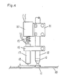
- the reference numeral 11 represents a chip part
- numeral 12 designating a nozzle for absorbing the chip part 11, said nozzle 12 thus forming a chip part holding device
- numeral 13 depicting a hollow sliding shaft having the nozzle 12 at an end thereof which is guided by means of sliding bearings 14 to be slidable upwardly and downwardly
- numeral 15 representing a tube connecting between the sliding shaft 13 and a vacuum source.
- a differential transformer 17 is fixedly secured to the sliding shaft 13 by means of a bracket 16.
- a needle 18 of the differential transformer 17 is secured through a compression spring 19 to a solenoid 20 which is in turn secured to the sliding shaft 13 by means of a bracket 21.
- the above-decribed absorbing section is allowed to run away upwardly by several millimeters.
- Designated at numeral 23 is a linear motor comprising a body 23A and a bobbin 23B having a wound wire.
- An application of a control signal to the bobbin 23B causes upward and downward movement of the sliding shaft 13 through a plate 24 mounted on the bobbin 23B.
- Numeral 25 represents a detector for detecting a position of the bobbin 23B in terms of height.
- the linear motor body 23A is fixedly secured at an end of a X-Y drive unit 26 and is selectively located in a X-Y position.
- Numeral 27 designates a part supplying section for supplying a chip part and numeral 28 depicts a circuit board on which the chip part is mounted.
- Designated at 29 is a control unit including a microprocessor and a memory. The control unit 29 is arranged to position the linear motor body 23A on X and Y axes, control upward and downward movement of the sliding shaft 13, and perform ON-OFF control of part absorption.
- the X-Y drive unit 26 is driven such that the nozzle 12 is positioned above the part supplying section 27, and in response to the drive of the linear motor 23 the nozzle 12 is fallen and lifted after absorption of the chip part 11.
- the X-Y drive unit 26 is further driven so that the nozzle 12, having the chip part 11, is located at a mounting position above the circuit substrate 28. Thereafter, the nozzle 12 is fallen in order to mount the chip part 11 on the circuit substrate 28.
- current to the solenoid 20 is turned off whereby the needle 18 is dropped under the action of the compression spring 19.
- the differential transformer 17 is a well-known displacement sensor and is arranged such that its output voltage is varied in accordance with the displacement amount of the needle 18.
- the needle 18 is lifted in response to application of current to the solenoid 20, and the nozzle 12 is also lifted and transferred by means of the X-Y drive unit 26 to the position of a part to be subsequently mounted.
- the above-described operation is cyclically repeated, wherein the mounting height h is subsequently measured while mounting.
- Figs. 5(a) to 5(c) are diagrams showing the conditions when the chip part 11 is mounted on the circuit board 28 by the nozzle 12.
- Fig. 5(a) illustrates the condition that the chip part 11 is normally mounted
- Fig. 5(b) shows the condition that it is lengthwise mounted
- Fig. 5(c) shows the condition that it is not mounted because of absorption error.
- the distance between the under surface of the nozzle 12 and the circuit board 23 is h1
- upper and lower limits taking into account the thickness of the chip part and the dispersion in terms of the thickness of the chip part are respectively h3 and h2
- the relation between them is h3 ⁇ h1 ⁇ h2. Therefore, the cases other than the relation result in the mounting error of the chip part shown in Figs. 5(b) and 5(c).
- Fig. 6 is similar to Fig. 3 embodiment with the exception that it does not include the compression spring 22 on the sliding shaft 13 not to have the structure capable of setting free the sliding shaft 13 upwardly and further it does not include the detector for measuring a distance between the under surface of the nozzle 12 and the circuit board 28.
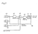
- Fig. 7 is a block diagram illustrating a section of the control unit 29 for controlling the linear motor 23 of Fig. 6.
- the reference numeral 40 represents a linear motor corresponding to the linear motor body 23A and the bobbin 23B of Fig. 6.
- Designated at numeral 41 is a position sensor for detecting the position of the bobbin 23B which corresponds to a device indicated by numeral 25 in Fig. 6.
- Numeral 42 depicts a power amplifier for driving the linear motor 40
- numeral 43 representing a preamplifier
- numeral 44 designates a D/A converter for converting a position command (digital signal) from the control unit into an analog signal.
- numeral 45 represents an A/D converter for converting a position feedback signal (analog signal) 46 for measurement of position into a digital signal
- numeral 47 representing a D/A converter for converting a load command (digital signal) from the control unit into an analog signal
- numeral 48 designating a mode changing switch for selecting either of the position control or load control of the linear motor 40.
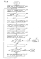
- Fig. 8 is a flow chart for the operation of mounting of the chip part. Hereinbelow, the operation will be described with reference to the figure.
- a step 101 the nozzle 12 is moved to the part position above the part supplying section 27 by means of the X-Y drive unit 26.
- a step 102 is executed to fall the nozzle 12, followed by a step 103 in which the chip part 11 is absorbed thereby and a step 104 in which the nozzle 12 is lifted with the absorbed chip part 11.
- the nozzle 12, in a step 105, is moved to the mounting position above the circuit board 28, followed by a step 106 in which the nozzle 12 is dropped up to the position that is separated by 0.5 to 1 mm from the mounting position of the chip part 11.
- a subsequent step 107 is executed to switch the mode changing switch 48 to the load control mode, followed by a step 108 wherein the nozzle 12 is fallen in accordance with command load.
- the position feedback signal 46 from the position sensor 41 is A-D converted by the A/D converter 45 and measured is a dropping amount of the nozzle 12 secured through the sliding shaft 13 and the plate 24 to the bobbin 23B.
- the dropping amount of the nozzle 12 is Hd and the distance between the lifted position of the nozzle 12 and the circuit board 28 is He
- a step 110 is provided for comparing h1 with h2 and h3 indicated in Fig. 5(a), and in accordance with the result of the comparison either of step 111 or 114 is executed. If the determination is made as an abnormal mounting of the part, the step 114 is executed to lift the nozzle 12, followed by a step 115 in which an error process is performed. On the other hand, if normal, the step 111 is executed such that the nozzle 12 is lifted. The step 111 is followed by a step 112 which is provided for checking whether the mounting to the circuit board is perfectly terminated. The termination causes the end of this operation, while no termination results in executing a step 113 wherein the nozzle 12 is moved to the position of the part which will be subsequently mounted. Thereafter, the operational flow returns to the step 102.
- This embodiment as compared with the first embodiment, is arranged such that the height h1 on the mounting of the chip part 11 is calculated on the basis of the output of the position sensor 25 necessary for the upward and downward drive control of the bobbin 23B by the linear motor 23.
- the part height h1 is calculated by measuring the dropping amount of the nozzle 12 on part mounting on the basis of the feedback signal 46 from the position sensor 41 for the upward and downward drive source of the chip part maintaining section which feedback signal 46 is A-D converted into a digital signal by means of the A/D converter 45, it is possible to detect the height on the chip part mounting without providing a detector for detecting the part height at a moving portion, resulting in reduction in cost.
- an optical length measuring device can be used. It is appropriate to use any device which is capable of measuring the distance between the under surface of the nozzle 12 and the circuit board 28.
- an analog output sensor has been used, however, it is possible to use a digital putput sensor of optical type or magnetic type. In this case, there is no need for using the A/D converter 45.
- the height of a chip part is detected when the chip part is mounted and the part mounting is directly confirmed by comparing the detection value with the range of dispersion in terms of the thickness of the chip part. Therefore, it is possible to increase the reliability of the mounting detection and to simplify the system maintenance, resulting in large practical effect.
Applications Claiming Priority (2)
| Application Number | Priority Date | Filing Date | Title |
|---|---|---|---|
| JP59186770A JPH07101797B2 (ja) | 1984-09-06 | 1984-09-06 | 電子部品装着方法 |
| JP186770/84 | 1984-09-06 |
Publications (3)
| Publication Number | Publication Date |
|---|---|
| EP0195820A1 EP0195820A1 (en) | 1986-10-01 |
| EP0195820A4 EP0195820A4 (en) | 1987-10-01 |
| EP0195820B1 true EP0195820B1 (en) | 1991-08-28 |
Family
ID=16194323
Family Applications (1)
| Application Number | Title | Priority Date | Filing Date |
|---|---|---|---|
| EP85904287A Expired - Lifetime EP0195820B1 (en) | 1984-09-06 | 1985-08-30 | Method of mounting electronic parts and an apparatus therefor |
Country Status (6)
| Country | Link |
|---|---|
| US (1) | US4790069A (ja) |
| EP (1) | EP0195820B1 (ja) |
| JP (1) | JPH07101797B2 (ja) |
| KR (1) | KR900000184B1 (ja) |
| DE (1) | DE3583939D1 (ja) |
| WO (1) | WO1986001676A1 (ja) |
Families Citing this family (16)
| Publication number | Priority date | Publication date | Assignee | Title |
|---|---|---|---|---|
| US4705311A (en) * | 1986-02-27 | 1987-11-10 | Universal Instruments Corporation | Component pick and place spindle assembly with compact internal linear and rotary displacement motors and interchangeable tool assemblies |
| JPH0746760B2 (ja) * | 1986-03-10 | 1995-05-17 | 松下電器産業株式会社 | 電子部品装着方法 |
| JP2770457B2 (ja) * | 1989-08-02 | 1998-07-02 | 松下電器産業株式会社 | 電子部品実装方法 |
| FR2661630B1 (fr) * | 1990-05-04 | 1992-08-07 | Renault | Dispositif permettant le maintien et/ou l'assemblage automatique de pieces, comportant des bras porte-outils montes sur un bloc-support. |
| US5208975A (en) * | 1990-07-06 | 1993-05-11 | Matsushita Electric Industrial Co., Ltd. | Method and apparatus for mounting electronic parts |
| US5172469A (en) * | 1991-05-08 | 1992-12-22 | Hughes Aircraft Company | Advanced part removal and torque shear station |
| JPH0618215A (ja) * | 1992-07-01 | 1994-01-25 | Yamaha Motor Co Ltd | 部品装着方法及び装置 |
| US5365657A (en) * | 1993-02-01 | 1994-11-22 | Advanced Interconnection Technology | Method and apparatus for cutting wire |
| US5331831A (en) * | 1993-03-19 | 1994-07-26 | Bermo, Inc. | Hardware sensor |
| JP3086578B2 (ja) * | 1993-12-27 | 2000-09-11 | ヤマハ発動機株式会社 | 部品装着装置 |
| JP3090567B2 (ja) * | 1993-12-29 | 2000-09-25 | ヤマハ発動機株式会社 | 実装機における部品認識方法および同装置 |
| JP3301304B2 (ja) * | 1996-03-28 | 2002-07-15 | 松下電器産業株式会社 | 電子部品実装装置および電子部品実装装置におけるノズル交換方法 |
| KR100585145B1 (ko) * | 2004-06-05 | 2006-05-30 | 삼성전자주식회사 | 제트 레벨에 의한 리젝트 프레임 판별 시스템 및 이를 이용한 와이어 본딩 방법 |
| KR101047033B1 (ko) * | 2009-07-23 | 2011-07-06 | (주) 에스에스피 | 공정거리 설정이 편리한 자동화 조립장비 및 이를 이용한 공정거리 설정방법 |
| JP5750235B2 (ja) | 2010-04-29 | 2015-07-15 | 富士機械製造株式会社 | 製造作業機 |
| CN102934540B (zh) | 2010-04-29 | 2015-09-30 | 富士机械制造株式会社 | 制造作业机 |
Family Cites Families (9)
| Publication number | Priority date | Publication date | Assignee | Title |
|---|---|---|---|---|
| GB912578A (en) * | 1959-05-14 | 1962-12-12 | Pye Ltd | Machine for handling semiconductor material |
| US3670388A (en) * | 1969-12-29 | 1972-06-20 | Teletype Corp | Self-testing insertion tool and methods of inserting workpieces |
| JPS5726835B2 (ja) * | 1973-03-08 | 1982-06-07 | ||
| JPS50126453A (ja) * | 1974-03-25 | 1975-10-04 | ||
| JPS55162299A (en) * | 1979-07-05 | 1980-12-17 | Pioneer Electronic Corp | Device for transferring electronic part mounting unit |
| FR2479641A1 (fr) * | 1980-03-25 | 1981-10-02 | Numergo Sa | Atelier flexible permettant la digitalisation et le cablage de circuits electroniques hybrides |
| US4501064A (en) * | 1981-09-08 | 1985-02-26 | Usm Corporation | Micro component assembly machine |
| JPS59198800A (ja) * | 1983-04-26 | 1984-11-10 | 株式会社デンソー | マルチヘツド部品組付装置 |
| US4510683A (en) * | 1983-10-27 | 1985-04-16 | Sperry Corporation | Force assembler apparatus for robots |
-
1984
- 1984-09-06 JP JP59186770A patent/JPH07101797B2/ja not_active Expired - Lifetime
-
1985
- 1985-08-28 KR KR1019850006214A patent/KR900000184B1/ko not_active IP Right Cessation
- 1985-08-30 WO PCT/JP1985/000480 patent/WO1986001676A1/ja active IP Right Grant
- 1985-08-30 US US06/862,226 patent/US4790069A/en not_active Expired - Lifetime
- 1985-08-30 DE DE8585904287T patent/DE3583939D1/de not_active Expired - Lifetime
- 1985-08-30 EP EP85904287A patent/EP0195820B1/en not_active Expired - Lifetime
Also Published As
| Publication number | Publication date |
|---|---|
| DE3583939D1 (de) | 1991-10-02 |
| JPH07101797B2 (ja) | 1995-11-01 |
| EP0195820A4 (en) | 1987-10-01 |
| JPS6164200A (ja) | 1986-04-02 |
| KR900000184B1 (ko) | 1990-01-23 |
| US4790069A (en) | 1988-12-13 |
| KR860002943A (ko) | 1986-04-30 |
| EP0195820A1 (en) | 1986-10-01 |
| WO1986001676A1 (en) | 1986-03-13 |
Similar Documents
| Publication | Publication Date | Title |
|---|---|---|
| EP0195820B1 (en) | Method of mounting electronic parts and an apparatus therefor | |
| KR960015922B1 (ko) | 다이본딩장치 | |
| JP5095084B2 (ja) | 試料の表面形状の測定方法及び装置 | |
| EP0368533A2 (en) | Quality control for wire bonding | |
| JP2006226964A5 (ja) | ||
| US6282779B1 (en) | Device and method for mounting electronic parts | |
| EP0011952B1 (en) | Method and apparatus for testing enclosed electromagnetic relays | |
| EP0745858A1 (en) | Acceleration sensor | |
| US4813123A (en) | Method of adjusting an electric horn air gap | |
| KR20010075433A (ko) | 피크-앤-플레이스 로봇 내에서 기판 상에 배치된 소자의위치를 검출하는 방법 | |
| CA2545146C (en) | Failure detecting device for elevator drive power source and failure detecting method for elevator drive power source | |
| US6119917A (en) | Wire bonding apparatus and bonding load correction method for the same | |
| US6583637B2 (en) | Load-control-type actuator | |
| JPH09318468A (ja) | 接圧力測定装置および開閉器 | |
| KR20040047628A (ko) | 호일로부터 반도체칩을 파지하는 방법 | |
| JPH06132698A (ja) | 電子部品装着装置 | |
| JPH09236530A (ja) | 超微小硬度測定装置 | |
| JP3233053B2 (ja) | 電子部品実装装置における移載ヘッドのノズルの高さ計測方法 | |
| US6049203A (en) | Apparatus and method for testing an inker of the semiconductor wafer probe station | |
| KR100261501B1 (ko) | 본딩하중 조절을 위한 접촉감지방법 | |
| JPH11138747A (ja) | スクリーンはんだ付けのはんだ残量検知ユニットおよびスクリーンはんだ付けのはんだ残量検知方法 | |
| JPH11304837A (ja) | プローブ装置 | |
| KR920005430B1 (ko) | 엘리베이터의 정지위치 검출장치 및 방법 | |
| JPH0943092A (ja) | 加速度センサの衝撃試験方法及びその装置 | |
| JPH0572153A (ja) | クリームはんだのはんだ付け性測定装置 |
Legal Events
| Date | Code | Title | Description |
|---|---|---|---|
| PUAI | Public reference made under article 153(3) epc to a published international application that has entered the european phase |
Free format text: ORIGINAL CODE: 0009012 |
|
| 17P | Request for examination filed |
Effective date: 19860505 |
|
| AK | Designated contracting states |
Kind code of ref document: A1 Designated state(s): DE GB |
|
| A4 | Supplementary search report drawn up and despatched |
Effective date: 19871001 |
|
| 17Q | First examination report despatched |
Effective date: 19890901 |
|
| GRAA | (expected) grant |
Free format text: ORIGINAL CODE: 0009210 |
|
| AK | Designated contracting states |
Kind code of ref document: B1 Designated state(s): DE GB |
|
| REF | Corresponds to: |
Ref document number: 3583939 Country of ref document: DE Date of ref document: 19911002 |
|
| PLBE | No opposition filed within time limit |
Free format text: ORIGINAL CODE: 0009261 |
|
| STAA | Information on the status of an ep patent application or granted ep patent |
Free format text: STATUS: NO OPPOSITION FILED WITHIN TIME LIMIT |
|
| 26N | No opposition filed | ||
| PGFP | Annual fee paid to national office [announced via postgrant information from national office to epo] |
Ref country code: GB Payment date: 19970821 Year of fee payment: 13 |
|
| PGFP | Annual fee paid to national office [announced via postgrant information from national office to epo] |
Ref country code: DE Payment date: 19970905 Year of fee payment: 13 |
|
| REG | Reference to a national code |
Ref country code: GB Ref legal event code: 746 Effective date: 19970901 |
|
| PG25 | Lapsed in a contracting state [announced via postgrant information from national office to epo] |
Ref country code: GB Free format text: LAPSE BECAUSE OF NON-PAYMENT OF DUE FEES Effective date: 19980830 |
|
| GBPC | Gb: european patent ceased through non-payment of renewal fee |
Effective date: 19980830 |
|
| PG25 | Lapsed in a contracting state [announced via postgrant information from national office to epo] |
Ref country code: DE Free format text: LAPSE BECAUSE OF NON-PAYMENT OF DUE FEES Effective date: 19990601 |