EP0194331B1 - Einrichtung zum Überprüfen von Abdrücken - Google Patents
Einrichtung zum Überprüfen von Abdrücken Download PDFInfo
- Publication number
- EP0194331B1 EP0194331B1 EP85102956A EP85102956A EP0194331B1 EP 0194331 B1 EP0194331 B1 EP 0194331B1 EP 85102956 A EP85102956 A EP 85102956A EP 85102956 A EP85102956 A EP 85102956A EP 0194331 B1 EP0194331 B1 EP 0194331B1
- Authority
- EP
- European Patent Office
- Prior art keywords
- printed sheet
- differential
- line sensor
- signal
- Prior art date
- Legal status (The legal status is an assumption and is not a legal conclusion. Google has not performed a legal analysis and makes no representation as to the accuracy of the status listed.)
- Expired - Lifetime
Links
Images


Classifications
-
- B—PERFORMING OPERATIONS; TRANSPORTING
- B41—PRINTING; LINING MACHINES; TYPEWRITERS; STAMPS
- B41F—PRINTING MACHINES OR PRESSES
- B41F33/00—Indicating, counting, warning, control or safety devices
- B41F33/0036—Devices for scanning or checking the printed matter for quality control
-
- G—PHYSICS
- G01—MEASURING; TESTING
- G01N—INVESTIGATING OR ANALYSING MATERIALS BY DETERMINING THEIR CHEMICAL OR PHYSICAL PROPERTIES
- G01N21/00—Investigating or analysing materials by the use of optical means, i.e. using sub-millimetre waves, infrared, visible or ultraviolet light
- G01N21/84—Systems specially adapted for particular applications
- G01N21/88—Investigating the presence of flaws or contamination
- G01N21/95—Investigating the presence of flaws or contamination characterised by the material or shape of the object to be examined
- G01N21/956—Inspecting patterns on the surface of objects
-
- H—ELECTRICITY
- H04—ELECTRIC COMMUNICATION TECHNIQUE
- H04N—PICTORIAL COMMUNICATION, e.g. TELEVISION
- H04N1/00—Scanning, transmission or reproduction of documents or the like, e.g. facsimile transmission; Details thereof
- H04N1/00002—Diagnosis, testing or measuring; Detecting, analysing or monitoring not otherwise provided for
- H04N1/00026—Methods therefor
- H04N1/00037—Detecting, i.e. determining the occurrence of a predetermined state
Definitions
- the present invention relates to an inspecting device for print for detecting a defect occurred on the printed sheet by comparing the state of the printed sheet during printing with a reference state in a printing machine.
- printed sheets have been inspected one by one by a human examiner in an off-line step. This is because even printed sheets of the same pattern are slightly different due to replenishing ink, changes in the ambient temperature, minor troubles in the printing machine, etc. Only the human visual sense can detect such delicate differences.
- this system still has some problems. As one of the major causes, there is a phenomenon that the color density of a printed sheet entirely varies even in normal operation duee to the characteristics of a printing machine. In this system which merely compares the color density of the print with reference information, it is difficult to judge such defects of the printed sheet. The entire variation in the color density is caused by the inking mechanism, irregularities in the water supply amount of a damping unit and alterations in the. ink amount of an ink source, and it is very difficult to suppress such variations in the color density within a predetermined value.
- a printed web to be inspected is affected by the influence of variations in the tension, feeding velocity and drying temperature, so that the web fed in a web rotary press shows fine speed variations in the feeding direction.
- the difficulty of the accurate synchronization means different pixels to be inspected in the respective picture patterns of the printed web, and an accurate inspection cannot be fundamentally achieved in the system for inspecting a defect by comparing the print with reference information for each pixel.
- a printed sheet to be inspected is printed with black, cyan, magenta and yellow ink in the ordinary color printing. Even when a printing defect occurs only in one of these colors, the inspecting device must be capable of detecting the defect.
- a device has been proposed so far having the features of separating the signal light from the printed sheet into wavelength bands by utilizing three color separation filters of R (red: wavelengths of 600-700 nm), G (green: wavelengths of 500-600 nm), and B (blue violet: wavelengths of 400-500 nm), respectively inputting the three wavelength bands into three CCD cameras, inputting the three wavelength bands into a CCD camera by rotating the R, G, and B filters to process the R, G and B signals in a time series, or alternatively flashing light sources of R, G and B to provide similar effects.
- R red: wavelengths of 600-700 nm
- G green: wavelengths of 500-600 nm
- B blue violet: wavelengths of 400-500 nm
- GB-A 2 044 925 discloses an inspecting device which is adapted for the detection of defects in regular patterns.
- the output signal of a scanner scanning the print pattern is delayed by an amount equal to the pitch of the print pattern.
- This delayed scan signal is copared with the actual undelayed scan signal and an error detection signal is generated when a difference between these signals indicating a defect lying between the print raster positions is detected.
- the inspecting device according to the invention allows an accurate detection even if an entire variation in a color density occurs in a print picture of the printed sheet.
- Fig. 1 is a schematic diagram showing an inspecting device for a print according to the present invention.
- the inspecting device is mounted on a web rotary press, but may also be mounted in a sheet-fed press without any problems.
- a web print sheet 3 supplied from a rolled sheet 2 is printed on the front and back surfaces with four colors (black, cyan, magenta and yellow) in a printing unit 1, and then conveyed to a drier and a folding unit (not shown).
- the inspecting device scans image information of the entire print pattrn by a line sensor such as a CCD of an optical detecting device 4 in a direction perpendicular to the sheet feeding direction one by one along scanning lines while taking the timing of sampling by a rotary encoder 5 mounted in the printing unit 1 to input the image information to a processing circuit 6 at each pixel, compares, by means of the processing circuit 6, the image information with reference information, and judges whether the printed state is normal or abnormal, so as to inspect the printed state of the printed sheet.
- suitable means such as an alarm, marking means or a rejection means.
- Fig. 2 shows the construction of the optical detecting device 4.
- the detecting device 4 has a light source 7 for illuminating the printed sheet, on which prints of the print pattern 3' are sequentially printed on the sheet 3 and a line sensor camera 8 for receiving light reflected from the printed sheet and photoelectrically converting the reflected light.
- the light source 7 may use a xenon lamp, a halogen lamp, or a fluorescent lamp which is fired by a DC or a high frequency voltage.
- the camera 8 may utilize a CCD line sensor or a MOS line sensor. When a close contact line is used, an optical system can be simply adjusted, and the space may be saved.
- Reference numeral 9 designates a scanning line of the camera 8, which is perpendicular to the feeding direction D of the printed sheet.
- an example of the spectral sensitivity curve of the CCD line sensor is understood to have, as shown in Fig. 3, a low sensitivity in the B component of the wavelength band of 400-500 nm and having a peak at 700 nm in such a manner that the curve of the spectral sensitivity ratio of B component: G component: R component is equal to 1:13:1.5.
- Fig. 3 shows the spectral sensitivity curve of the CCD line sensor, and the MOS type line sensor has a similar spectral sensitivity curve to that of the CDD line sensor.
- the spectral sensitivity ratio of the CCD line sensors of BN, G an R components is equal to 1:11.3:1.5 as described above, and when the ouput ratio of the white portion of the printed sheet of the CCD line sensor to the printed portion of 100% dots of the respective inks is obtained from this ratio and the ratio of the white portion of the printed sheet to the B, G and R components of the printed portion of 100% dots of the inks as listed in Table 1 in case that the white portion is 1, the ratio becomes as below.
- the yellow ink has only 0.22 of the output difference from the white portion of the printed sheet even on the printed portion of 100% dots.
- the printing defect of the yellow ink must be detected in the state that range of output level is much lower than those of other inks.
- the output of the CCD line sensor by the variation in the yellow ink is 1/2 or lower of that by the variation in the cyan ink in response to the above-mentioned output ratio.
- an optical filter 10 which has a spectral transmission characteristic having a peak in the transmission factor in the wavelength band of 400 to 500 nm is disposed as means for equalizing the outputs of the line sensors for the repsectively color inks between the line sensor camera 8 an the printed sheet.
- the light reflected from the printed sheet, which is illuminated by the light source 7, is incident through the filter 10 on the camera 8 to sufficiently provide an output of the yellow ink different to that of the white portion of the printed sheet, thereby enhancing the detecting accuracy of the yellow ink as compared with the other inks in the same degree as the other inks.
- the optical filter 10 will be described in more detail.
- Fig. 5 shows the spectral transmission characteristic of the optical filter 10 of an embodiment according to the present invention.
- the filter 10 has, as spectral transmission characteristics, a 90% transmission factor of the B component (wavelength: 400-500 nm), a 10% transmission factor of the G component (wavelength: 500-600 nm), and a 20% transmission factor of the R component (wavelength: 600-700 nm).
- the transmission factor of the B component is 9 times as that of the G component, and 4.5 times as that of the R component, i.e., the ratio of the spectral transmission factors is 9:1:2 as concrete values. The reason why such a ratio is provided will be described. It is noted that a peak exists in the transmission factor of the B component, and other components (R, G) have larger transmission factors than the color separation filter (B) which is used generally.
- the mean transmission factors of the optical filter in the wavelengths of 400 to 500 nm, 500 to 600 nm and 600 to 700 nm are respectively represented by X1 , X2 and x 3 .
- the output of the CCD line sensor of the yellow ink can be obtained by the following formula from the spectral sensitivity ratio of the CCD line sensor and the spectral reflection characteristics of the yellow ink as described above:
- the outputs of the line sensor for the magenta and cyan inks can be obtained by the following formulae:
- the optical filter which has the spectral transmission factor as shown in Fig. 5 can be provided by designing the actual optical filter on the basis of the spectral transmission factor ratio of 9:1:2 to be incorporated.
- the output ratio of the CCD line sensors becomes as below.
- the outputs of the line sensors for the respective color inks can be equalized in balance, and an output ratio of sufficiently high difference between the white portion of the printed sheet and the other color inks can be provided. Consequently, similarly high detecting accuracy can be provided in the line sensors for the respective color inks.
- This example depends upon the spectral sensitivity curve of the CCD line sensor shown in Fig. 3 and the spectral reflection curve of the ink shown in Fig. 4.
- other line sensors or other types of inks are substantially similar in the curves as shown in Fig. 3 and/or Fig. 4, and the difficulty in the detection of the printing defect of the yellow ink is still similar so that the optical filter as described above is advantageous in detecting printing defects in yellow ink.
- the optical filter has a peak in the transmission factor of 400 to 500 nm of the wavelength band and the spectral transmission curve has a transmission factor of the degree capable of obtaining the necessary output for detecting the printing defect in other visible light wavelength bands, the difficulty in the detection of the printing defect of the yellow ink can be eliminated.
- the filter had a transmission factor of the B component of approximately twice as that of the other component, the output ratio of the line sensor can be remarkably improved by means of this optical filter and the difficulty in the detection of the printing defect of the yellow ink can be obviated.
- Fig. 6 shows the spectral curve d of the No. 38 and the spectral curve e of No. 79. Both curves have peaks in the transmission factor of the B component and the transmission factors of the B components of these filters are twice or more than those of the G and R components, and the transmission factors of G and K components are sufficient for detecting the other color ink.
- the line sensor causes an oozing phenomenon in an infrared ray (wavelength: 700 nm or higher).
- Table 2 shows the outputs of a CCD line sensor measured in case that only the infrared cut-off filter and the combination of No. 38 of the optical filter an the infrared cut-off filter are mounted between the CCD line sensor and the respective color inks are printed in 100% dots.
- the quantity of light is reduced by the use of the filter of No. 38, but the gain is adjusted by an amplifier, and the output level of the line sensor from the white portion of the printed sheet are equalized between only infrared cut-off filter and combination of No. 38 and infrared cut-off filter.
- the output difference of the line sensor between the yellow ink and the white portion of the printed sheet becomes 2.5 times by employing the filter of No. 38, and the detecting accuracy of the line sensor with the above-mentioned optical filter can be remarkably improved as compared with the conventional line sensor with only the infrared cut-off filter.
- the output difference of the line sensor between the magenta ink and the white portion of the printed sheet becomes approximately 1.7 times, and a similar advantage can be provided.
- the output difference of the line sensor between the cyan ink and the white portion of the printed sheet becomes 0.75 times, which is still higher than the magenta ink and causes no problem in the detection.
- the image information of the print pattern input by the optical detecting device 4 as described above is fed to the processing circuit 6, which inspects the presence of defects occurred on the printed sheet 3.
- Fig. 7 shows a block diagram of the processing circuit 6.
- the rotary encoder 5 mounted in the printing machine is connected to a timing control circuit 200, which calculates a scan-starting pulse SP of the CCD line sensor camera 8 on the basis of a timing pulse TP from the encoder 5, and transforms the pulse SP to the camera 8.
- the pulse SP may directly utilize the pulse TP generated from the encoder 5, because out-of-synchronization caused by the infinitesimal variation in the feeding direction speed of the printed sheet does not occur in the sheet-fed press.
- the camera 8 is connected to an A/D converted 11, and transfers the image information of the print pattern of the printed sheet as analog information in a direction perpendicular to the feeding direction of the printed sheet at every pixel to the converter 11 on the basis of the pulse SP.
- the converter 11 is connected to a data control circuit 14, converts the analog image information transferred from the camera 8 into a digital signal at every pixel, and transfers the digital signal to the control circuit 14.
- the data control circuit 14 receives and delivers the digital image information to a bus line 20 as inspecting information, and has functions of accelerating the data transfer, controlling the timing of receiving and delivering the data, and buffering the data.
- a reference memory 15 is connected to the bus line 20 and stores reference information at every pixel as reference for the inspection.
- the operator instructs inputting of the reference information on an operation panel 12, and the print pattern information input from the camera 8 is resultantly stored in the memory 15 through the converter 11 and the control circuit 14 described above.
- the memory 15 and a previous value memory 16 are controlled by a memory control circuit 19 for storing the data and reading out the data.
- the operation panel 12 is connected to an external interface 18 to instruct the entire inspecting device.
- the instruction signal is transferred through the interface 18 to a CPU board 17, which controls the circuits in accordance with a program stored therein.
- the processing circuit 6 When the reference information is stored in the memory 15, the processing circuit 6 is shifted to an inspection mode.
- the inspection mode the image information of the print pattern of the printed sheet which is sequentially printed is delivered from the camera 8 through the converter 11 and the control circuit 14 to an error-judging circuit 100 as the information to be inspected.
- the reference informaton in the same address as the information to be inspected is simultaneously delivered from the memory 15 to the error judging circuit 100, which compares and calculates the information to be inspected with the reference information to detect errors or defects occured on the print pattern of the printed sheet.
- the judging circuit judges the presence of the defect, an error signal is transferred to the CPU board 17, which thus operates alarm means such as a display unit, a marking unit or a rejecting unit through the interface 18, thereby notifying the operator of the printing machine of the presence of the defect.
- the error judging circuit 100 judges the defect, it is required to accurately inspect the defect by eliminating the influence of the variation in the color density of the entire printed sheet as described above.
- Fig. 9 shows an example of the case that variations in the color density occur on the print pattern of the entire printed sheet.
- Fig. 9 is a graph illustrating the measured reflection density (through R filter) of 100% dots of cyan of the printed sheet at every 1000 sheets aftr printing starting.
- the reference color density of 100% dots of cyan is 1.3 to 1.4 as designated by a broken line, while it is understood from Fig. 9 that the actual variation in the color density of the printed sheet as designated by a solid line is very large.
- the causes for the variation in the color density include the quantity of inks in ink fountains, the periodicity of supplying inks through an ink roller arrangement, balance with dampening water, the content of the print pattern, etc. It is said to be very difficult at present to suppress the variation in the color density by obviating the respective causes one by one.
- Figs. 10 shows a printing defect in the inspection of a printed sheet in a model.
- Fig. 10(A) shows the image information at every pixel in case that a printing defect such a dripped water or oil occurs on a printed sheet by a one-dotted line and the reference information at the normal time by a solid line.
- Fig. 10(B) shows the image information at every pixel in case that stains occur as a printing defect on the printed sheet by a one-dotted chain line an the reference information at the normal time by a solid line.
- Fig. 11 (A) and Fig. 11(B) broken lines are threshold levels, and a solid line is the value of the difference between the detected image information and the reference information.
- the printing defect can be inspected by setting upwardly the level of the threshold value, but when the entire variation in the color density increases more, the entire signal exceeds the threshold level to cause an impossibility in judging, or even if the width of the variation in the signal due to the printing defect is extended to the width of the entire variation in the color ensity so that such a remarkable printing defect does not cause the signal to exceed the threshold level, thereby possibly disabling the detection of printing defects.
- the threshold value is set to the twice differential signal produced by taking the difference between the differential signal (e.g., the signal designated by the solid line in the model in Fig. 11) produced by taking the difference between the detected image information and the reference information and a signal displaced (delayed) by several pixels (3 to 5 pixels) from the differential signal in the scanning direction.
- the differential signal e.g., the signal designated by the solid line in the model in Fig. 11
- Figs. 12 show the twice differential signals processed as described above.
- Fig. 12(A) shows the signal shown in Fig. 11 (A) processed as described above
- Fig. 12(B) shows the signal shown in Fig. 11(B) similarly processed as described above.
- the presence of the printing defect can be judged (i.e., setting the threshold level) in the state that the influence of the entire variation in the color density is eliminated by the above-mentioned process.
- the twice differential signal produced by the above-mentioned process results in the similarity apparently to the signal produced by analog differentiating the analog differential signal produced by taking the difference between the detected image information and the reference information, but has the following large advantages as compared with the process by the analog differentiation.
- a leakage phenomenon to adjacent pixels occurs in the rise and fall of the color density of the print pattern in the CCD line sensor for inspecting the printing defect with respect to the density pattern DP of the print pattern, and the signal is output in the insensitive state as designated by a pattern OP.
- this signal is differentiated, a signal difference is not almost presented as shown in Fig. 14 even if the original signal has a considerably signal difference, the varying points are concealed by the influence of the entire variation in the color density described above, and the printing defect cannot be resultantly inspected.
- printing defects occurring slowly in the variation in the color density can also be accurately detected at the color density varying point of the printing defects of the entire variation in the color density of the printed sheet by alleviating the influence of the oozing phenomenon of the CCD line sensor or the MOS line sensor.
- the preferable number of delaying pixels is 3 to 5.
- the differential value of the signal produced by taking the difference between the color density detection information from the print pattern of the printed sheet and the reference information is accumulated in advance in the amount corresponding to a predetermined number of pixels, the reference values of the upper and lower limits to the accumulated value are set, and when the accumulated value exceeds the reference value, it is judged that an entire abnormal variation in the color density occurs.
- a printing defect such as dripped water or oil, and stains can be detected and the entire abnormal variation in the color density can also be preferably detected by adding the second process described above to the previous first process.
- the error-judging circuit 100 working as described above, has a circuit arrangement shown in Fig. 8, and will now be described in detail with reference to Fig. 8.
- the error judging circuit 100 calculates the difference between the image information and the reference information by a first differential circuit 101 and produces a first differential signal DIS.
- This signal DIS corresponds to the signal designated by the solid line in Fig. 11.
- the first differential circuit 101 is connected to the second differential circuit 102, a delay circuit 103 and an accumulation counter 106.
- the delay circuit 103 produces a delay signal DDS delayed by 3 to 5 pixels from the differential signal DIS in the scanning direction, and is connected to the second differential circuit 102.
- the second differential circuit 102 calculates the difference between the signal DIS and the delay signal DDS, and produces a twice differential signal SDS.
- This signal SDS corresponds to the signal designated by the solid line in Fig. 12.
- the second differential circuit 102 is connected to an absoluteizing circuit 104, and the twice differential signal SDS produced by the differential circuit 102 is absoluteized by the circuit 104.
- the absoluteization of the twice differential signal SDS means that the inspection is executed by one comparing circuit without providing two upper and lower limit comparing circuits. When the two comparing circuits are provided, the absoluteizing circuit 104 can be eliminated.
- the absoluteizing circuit 104 is connected to a first comparing circuit 105, which judges whether the absoluteized second differential signal is larger than a threshold level signal SH1 or not.
- the signal SH1 is applied from the CPU board 17, and may be fixed or variable depending upon the magnitude of the reference information.
- the signal DIS from the circuit 101 is accumulated in the counter 106 for one print pattern.
- the counter 106 is connected to the absoluteizing circuit 107, which absoluteizes an accumulation count signal ICS.
- the absoluteizing circuit 107 is to operate with only one comparing circuit as described above.
- the absoluteizing circuit 107 is connected to a second comparing circuit 108, which compares the absoluteized accumulation count signal with a threshold level signal SH2, and transfers an error signal ER 2 to the CPU board 17 when the signal ICS exceeds the signal SH2.
- the signal SH2 applied from the CPU board 17 may be fixed or may be arbitrarily set.
- the counter 106 is reset when one print pattern of the printed sheet is completely inspect.
- the circuit 100 can accurately inspect the printed sheet even if an entire variation in the color density occurs on the printed sheet to be inspected by comparing the second differential signal with an allowable value.
- a delicate speed variation occurs in the feeding direction of web-printed sheet as described above, and there arises a problem of out-of-synchronization in case of inputting print pattern information.
- the out-of-synchronization as shown in Fig. 18 means a phenomenon that a scanning line for sampling in according with the timing pulse from the rotary encoder becomes different at every signal inputting time.
- print pattern information is input along scanning lines of n, n+1,... during scanning of a certain print pattern of the printed sheet, but the information becomes print pattern information along scanning lines of n', n'+1, ... during the next scanning of print pattern of the printed sheet.
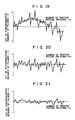
- Fig. 19 shows a graphical diagram of the measured result (synchronizing characteristic) of the displacement of synchronization of a printing machine at the normal operation time (400 rpm) is a model manner.
- the variation in speed is converted to the print pattern, there is an irregularity of approximately several mm of displacement with respect to the reference length. It is understood that this irregularity results from the combination of the large periodic wave over several hundreds of the number of print patterns and the small periodic wave of the face that the displacements alternatively become large and small at every other print pattern, and ranges in approximately several mm.
- the influence of the long periodic wave of several hundreds of the number of the print patterns of the variations of the displacement of the synchronization shown in Fig. 19 is eliminated.
- a plurality of print patterns are used as a set (e.g., 5 to 20 print patterns are used as a set), the average value (designated by a broken line) of the displacement of the synchronization is calculated, and then fed back, and the displacement of the synchronization of the one periodic length of one print pattern of next set is corrected.
- the influence of the long periodic wave can be substantially eliminated.
- a scan starting signal SP for scanning once per 10 pulses is fed to the CCD line sensor camera 8 in 1000 pulses and 100 scans in the state that the displacement of synchronization is 0.
- the scanning lines are unstable due to the displacement of synchronization as shown in Fig. 22 as they are, and therefore large displacement occurs at every print pattern.
- the number of the print patterns of the printed sheet to take the average value of the displacements of synchronization is set to 10 sheets, and the average value of the displacement of synchronization per one print pattern is calculated.
- the average value of the displacements of synchronization per one print pattern of the printed sheet is calculated with a plurality of print patterns as a set, and the displacement of synchronization of the print patterns of a plurality of sheets of the next set is corrected. Then, the displacement of synchronization presented as a long and large periodic wave as shown in Fig. 20 can be eliminated.
- the influence of the short periodic wave at every several print patterns can be reduced to an ignorable degree.
- the scanning lines are n, n+1, n+2, ... for print pattern of the printed sheet in a certain scanning
- the scanning lines become n', n'+ 1, n' +1, ... in the scanning for the next print pattern, and the displacement is M mm.
- the imaginary scanning line is set to the intermediate between both the scanning lines by averaging the image information input by the two print patterns of the printed sheet, and the displacement of this case can be accordingly suppressed to M/2 mm.
- the number of the print patterns to be averaged to obtain the imaginary scanning line is two.
- the number of the print patterns is not limited to two, but may be three times or more.
- a printing defect due to dripped water might, for example, occurs only on the print patterns of several (3 to 5) of printed sheets.
- the number of print patterns to be averaged is preferably set to several by considering the occuring frequency of the print defect (dripped oil or water) occuring at random on the print patterns of the printed sheet according to the density level.
- Fig. 21 shows the state that the averaging process (two print patterns are averaged) is executed by the above-mentioned method for the synchronizing characteristic of the state that the long periodic displacement of synchronization shown in Fig. 20 is eliminated.
- the displacement of synchronization is suppressed to approximately '/5 of the state shown in Fig. 19, the influence of the displacement of synchronization is not affected, and the improper synchronization can be obviated at this point.
- the improper synchronization can be suppressed to a level which is not defective in practical use, but, in the actual inspection of the printed sheet, the reference signal to be compared with the signal to be inspected is input from the normal printed sheet.
- the reference signal is input in the state of displacement of synchronization, the reference signal itself is not accurate, and the resultant inspection becomes meaningless.
- the inspecting device can compare the signal to be inspected with the reference signal and judge the printing defect in the state that the error in the detected signal due to the displacement of synchronization is minimized.
- Fig. 16 is a block diagram showing a timing control circuit arrangement of eliminating the displacement of synchronization of the above-mentioned long period.
- a timing pulse TP from the rotary encoder 5 is input to a counter 201, which counts the number of timing pulses TP for one print pattern of a printed sheet and outputs a count number CN.
- the counter 201 may be started and reset by the start of the print pattern, or a starting mark may be simultaneously printed on a printed sheet.
- the counter 201 is connected to a reference count memory 203 and a differential circuit 202.
- the memory 203 stores the count number CN of the timing pulses of the print pattern of the printed sheet when inputting the above-mentioned reference information.
- the memory 203 is connected to the differential circuit 202, and used as a reference count number SCN for comparing with the counted number of the print pattern to be inspected of the printed sheet after starting of the inspection.
- the differential circuit 202 calculates the difference between the count number CN of one print pattern during inspecting and the reference count number SCN, and transfers a differential count number DCN (corresponding to the displacement of synchronization) as the result to a differential count memory 204.
- the memory 204 stores the differential count number DCN in the amount corresponding to predetermined number of print patterns (10 patterns in the above example).
- the memory 204 is connected to an adder circuit 205, which calculates the sum of the count number DCN of the predetermined number of the print patterns.
- the adder 205 is connected to a divider circuit 206, which divides it by the predetermined number of print patterns, thereby producing an average value ADCN of the count number N (corresponding to the amount of displacement of synchronization for one print pattern). In this case, when the predetermined number is 2", a high calculating speed can be achieved by using a shifting circuit instead of the divider circuit.
- the count number SCN from the memory 203 is, on the other hand, transferred to the divider circuit 209, which divides the count number SCN by a predetermined scanning line number and produces a reference scanning interval pulse number SDN.
- the divider 209 is connected to a reference timing memory 208, which stores the pulse number SDN.
- the divider 209 and a reference timing memory 208 are connected to a timing correcting circuit 207, which counts a timing pulse TP for the print patterns of the next set on the basis of the reference scanning interval pulse number and the average value ADCN per one print pattern in one set and generates a scan starting pulse SP. In case that the average value ADCN is 0, the timing pulse TP is counted in the amount corresponding to the pulse number SDN, and a scan-starting pulse SP is generated.
- the scan-starting pulse SP is generated at an equal interval in the absolute value of the average value ADCN in one print pattern at an interval smaller by 1 than the pulse number SDN.
- the scan-starting pulse SP is generated at an equal interval in the absolute value of the average value ADCN in one print pattern at an interval larger by 1 than the pulse number SDN. Since these circuits have a margin in the calculating time for calculating at every one scan, an exclusive microprocessor is used and programmed.
- the pulse TP may be replaced with clocks shorter than the starting pulse.
- the CCD line sensor camera 8 can be scanned at the timing for eliminating the displacement of synchronization of a long period as shown in Fig. 20.
- the previous value memory 16 stores the D n-1(i,j) .
- an averaging circuit 300 inputs the image information N n(i,j) and the previous value signal D n-1(i,j) of the memory 16, and calculates by a differential circuit 301 a differential signal (V n(i. j) -D n-1(i, j) ).
- the differential circuit 301 is connected to a divider circuit 302 to produce the average value of the differential signal (V n(i,j) -D n-1(i,j) ).
- the output is not a mere average, but the differential circuit can calculate a weighted average.
- the divider 302 is connected to an adder circuit 303, which adds the signal D n-1(i, j ) and the average value transferred from the divider 302 and calculates the averaged signal D n(i, j) .
- the averaged signal D n(i,j) produced as described above is compared as the information to be inspected with the reference signal to average the detected image information at a timing axis, which means the same result as the inspection with respect to the imaginary scanning line of the print pattern of the printed sheet.
- the averaged signal D n(i, j) is stored in the memory 16, and utilized for the averaging with the detected image information V n+1(i, of the next print pattern of the printed sheet.
- the information to be inspected and input to the first differential circuit 101 may use the image information input from the CCD line sensor camera 8 in the state that no displacement of synchronization occurs (e.g. in a sheet-fed press) as it is, but when the averaged signal D n(i,j) produced by utilizing the timing control circuit 200, the averaging circuit 300 and the previous value memory 16 when a displacement of synchronization occurs (e.g., in a web rotary press), is used, the error judging circuit 100 can inspect in a state equivalent to the state that no displacment of synchronization occurs to accurately inspect the print pattern of the printed sheet.
Landscapes
- Engineering & Computer Science (AREA)
- General Health & Medical Sciences (AREA)
- Health & Medical Sciences (AREA)
- Life Sciences & Earth Sciences (AREA)
- Analytical Chemistry (AREA)
- Signal Processing (AREA)
- Quality & Reliability (AREA)
- Physics & Mathematics (AREA)
- Biomedical Technology (AREA)
- Chemical & Material Sciences (AREA)
- Multimedia (AREA)
- Biochemistry (AREA)
- General Physics & Mathematics (AREA)
- Immunology (AREA)
- Pathology (AREA)
- Inking, Control Or Cleaning Of Printing Machines (AREA)
- Investigating Materials By The Use Of Optical Means Adapted For Particular Applications (AREA)
Claims (8)
Priority Applications (3)
| Application Number | Priority Date | Filing Date | Title |
|---|---|---|---|
| DE8585102956T DE3578768D1 (de) | 1985-03-14 | 1985-03-14 | Einrichtung zum ueberpruefen von abdruecken. |
| EP85102956A EP0194331B1 (de) | 1985-03-14 | 1985-03-14 | Einrichtung zum Überprüfen von Abdrücken |
| US06/712,151 US4685139A (en) | 1985-03-14 | 1985-03-15 | Inspecting device for print |
Applications Claiming Priority (1)
| Application Number | Priority Date | Filing Date | Title |
|---|---|---|---|
| EP85102956A EP0194331B1 (de) | 1985-03-14 | 1985-03-14 | Einrichtung zum Überprüfen von Abdrücken |
Publications (2)
| Publication Number | Publication Date |
|---|---|
| EP0194331A1 EP0194331A1 (de) | 1986-09-17 |
| EP0194331B1 true EP0194331B1 (de) | 1990-07-18 |
Family
ID=8193371
Family Applications (1)
| Application Number | Title | Priority Date | Filing Date |
|---|---|---|---|
| EP85102956A Expired - Lifetime EP0194331B1 (de) | 1985-03-14 | 1985-03-14 | Einrichtung zum Überprüfen von Abdrücken |
Country Status (3)
| Country | Link |
|---|---|
| US (1) | US4685139A (de) |
| EP (1) | EP0194331B1 (de) |
| DE (1) | DE3578768D1 (de) |
Cited By (4)
| Publication number | Priority date | Publication date | Assignee | Title |
|---|---|---|---|---|
| DE4228904A1 (de) * | 1992-08-29 | 1994-03-03 | Heidelberger Druckmasch Ag | Verfahren zum Prüfen von Druckformen vor dem Druck |
| RU2109340C1 (ru) * | 1991-08-12 | 1998-04-20 | Кениг Унд Бауэр Аг | Способ оценки печатных изображений на носителе |
| RU2109341C1 (ru) * | 1991-08-12 | 1998-04-20 | Кениг Унд Бауэр Аг | Способ осуществления контроля качества изображений |
| RU2180621C2 (ru) * | 2000-05-11 | 2002-03-20 | Мрыхин Станислав Дмитриевич | Способ оптического измерения высоты контактного провода |
Families Citing this family (89)
| Publication number | Priority date | Publication date | Assignee | Title |
|---|---|---|---|---|
| US5144421A (en) * | 1954-12-24 | 1992-09-01 | Lemelson Jerome H | Methods and apparatus for scanning objects and generating image information |
| US4969038A (en) * | 1963-03-11 | 1990-11-06 | Lemelson Jerome H | Method for scanning image information |
| US4984073A (en) * | 1954-12-24 | 1991-01-08 | Lemelson Jerome H | Methods and systems for scanning and inspecting images |
| US5128753A (en) * | 1954-12-24 | 1992-07-07 | Lemelson Jerome H | Method and apparatus for scaning objects and generating image information |
| US4882764A (en) * | 1985-03-29 | 1989-11-21 | Quad/Tech, Inc. | Cutoff control system |
| US4885785A (en) * | 1986-10-31 | 1989-12-05 | Quad/Tech, Inc. | Cutoff control system |
| US4950911A (en) * | 1986-12-10 | 1990-08-21 | Process Automation Business, Inc. | Apparatus and method for inspecting sheet material |
| US4922337B1 (en) * | 1988-04-26 | 1994-05-03 | Picker Int Inc | Time delay and integration of images using a frame transfer ccd sensor |
| FR2633062B1 (fr) * | 1988-06-21 | 1992-11-27 | Dubuit Mach | Procede pour le controle de qualite d'une impression, et machine d'impression mettant en oeuvre un tel procede |
| USRE36047E (en) * | 1988-09-26 | 1999-01-19 | Picker International, Inc. | Multi-mode TDI/raster-scan television camera system |
| JPH02170279A (ja) * | 1988-12-23 | 1990-07-02 | Hitachi Ltd | 被検査対象パターンの欠陥検出方法及びその装置 |
| JPH0792853B2 (ja) * | 1989-06-19 | 1995-10-09 | 株式会社日本コンラックス | 紙葉類識別装置及び方法 |
| US5058175A (en) * | 1990-01-11 | 1991-10-15 | Mitsubishi Jukogyo Kabushiki Kaisha | Quality inspection method for a printed matter |
| JPH03223976A (ja) * | 1990-01-29 | 1991-10-02 | Ezel Inc | 画像照合装置 |
| JPH03224073A (ja) * | 1990-01-30 | 1991-10-03 | Ezel Inc | 位置合わせ装置 |
| ATE123443T1 (de) * | 1990-02-22 | 1995-06-15 | Komori Printing Mach | Apparat zur untersuchung von drucksachen und entsprechendes verfahren. |
| DE4012608A1 (de) * | 1990-04-20 | 1991-10-24 | Roland Man Druckmasch | Verfahren und vorrichtung zur bestimmung von passerdifferenzen an druckbildstellen eines mehrfarbenoffsetdruckes |
| US5144566A (en) * | 1990-06-14 | 1992-09-01 | Comar, Inc. | Method for determining the quality of print using pixel intensity level frequency distributions |
| US5181081A (en) * | 1990-09-06 | 1993-01-19 | Wea Manufacturing, Inc. | Print scanner |
| US5201395A (en) * | 1990-09-27 | 1993-04-13 | Oki Electric Industry Co., Ltd. | Bill examination device |
| EP0533305B1 (de) * | 1991-09-18 | 1997-08-27 | Komori Corporation | Verfahren und Gerät zum Nachweisen von fehlerhaften Drucksachen in einer Druckmaschine |
| CH684590A5 (de) * | 1991-09-26 | 1994-10-31 | Grapha Holding Ag | Verfahren zur Einheitlichkeitsprüfung von Druckbogen und Vorrichtung zur Durchführung desselben. |
| GB9120848D0 (en) * | 1991-10-01 | 1991-11-13 | Innovative Tech Ltd | Banknote validator |
| IT1250847B (it) * | 1991-10-15 | 1995-04-21 | Urmet Spa | Apparecchio per la validazione di banconote |
| US5321770A (en) * | 1991-11-19 | 1994-06-14 | Xerox Corporation | Method for determining boundaries of words in text |
| CA2077969C (en) * | 1991-11-19 | 1997-03-04 | Daniel P. Huttenlocher | Method of deriving wordshapes for subsequent comparison |
| US5440648A (en) * | 1991-11-19 | 1995-08-08 | Dalsa, Inc. | High speed defect detection apparatus having defect detection circuits mounted in the camera housing |
| JP3576570B2 (ja) * | 1991-11-19 | 2004-10-13 | ゼロックス コーポレイション | 比較方法 |
| US5841955A (en) * | 1991-12-02 | 1998-11-24 | Goss Graphic Systems, Inc. | Control system for a printing press |
| DE4217942A1 (de) * | 1992-05-30 | 1993-12-02 | Koenig & Bauer Ag | Druck-Qualitätskontrolleinrichtung für eine Schön- und Widerdruck-Rotationsdruckmaschine |
| GB2271080A (en) * | 1992-09-08 | 1994-04-06 | Tecscan Electronics Limited | Print monitor. |
| EP0612042B2 (de) * | 1993-02-17 | 2003-06-04 | Kba-Giori S.A. | Vorrichtung und Verfahren zum Prüfen von Drucksachen |
| FI95888C (fi) * | 1993-04-26 | 1996-04-10 | Valtion Teknillinen | Menetelmä painatuksen laadun valvomiseksi |
| WO1995000337A1 (en) * | 1993-06-17 | 1995-01-05 | The Analytic Sciences Corporation | Automated system for print quality control |
| DE4321177A1 (de) * | 1993-06-25 | 1995-01-05 | Heidelberger Druckmasch Ag | Vorrichtung zur parallelen Bildinspektion und Farbregelung an einem Druckprodukt |
| DE4321179A1 (de) * | 1993-06-25 | 1995-01-05 | Heidelberger Druckmasch Ag | Verfahren und Einrichtung zur Steuerung oder Regelung von Betriebsvorgängen einer drucktechnischen Maschine |
| DE4432371B4 (de) * | 1994-09-12 | 2004-12-09 | Heidelberger Druckmaschinen Ag | Verfahren zum Drucken und Weiterverarbeiten von Nutzen |
| US5812705A (en) * | 1995-02-28 | 1998-09-22 | Goss Graphic Systems, Inc. | Device for automatically aligning a production copy image with a reference copy image in a printing press control system |
| DE29507302U1 (de) * | 1995-05-05 | 1995-06-22 | MAN Roland Druckmaschinen AG, 63075 Offenbach | Rotationsdruckmaschine |
| US5767980A (en) * | 1995-06-20 | 1998-06-16 | Goss Graphic Systems, Inc. | Video based color sensing device for a printing press control system |
| US5805280A (en) * | 1995-09-28 | 1998-09-08 | Goss Graphic Systems, Inc. | Control system for a printing press |
| US5903712A (en) * | 1995-10-05 | 1999-05-11 | Goss Graphic Systems, Inc. | Ink separation device for printing press ink feed control |
| IT1284432B1 (it) * | 1996-03-22 | 1998-05-21 | De La Rue Giori Sa | Procedimento di controllo automatico della qualita' di stampa di un'immagine policroma |
| US5771811A (en) * | 1996-10-10 | 1998-06-30 | Hurletron, Incorporated | Pre-registration system for a printing press |
| US5828075A (en) * | 1996-10-11 | 1998-10-27 | Hurletron, Incorporated | Apparatus for scanning colored registration marks |
| GB2337327B (en) * | 1997-02-18 | 2000-11-15 | Raymond Charles Johnson | Apparatus and method for monitoring hand washing |
| US5999636A (en) * | 1997-10-10 | 1999-12-07 | Printprobe Technology, Llc | Apparatus and process for inspecting print material |
| JP2000036033A (ja) * | 1998-07-21 | 2000-02-02 | Toshiba Eng Co Ltd | 明暗検査装置および明暗検査方法 |
| US6335978B1 (en) | 1999-02-09 | 2002-01-01 | Moore North America, Inc. | Variable printing system and method with optical feedback |
| US6678067B1 (en) | 1999-04-06 | 2004-01-13 | Videk, Inc. | Automated document inspection system |
| JP2000326495A (ja) * | 1999-05-24 | 2000-11-28 | Matsushita Electric Ind Co Ltd | クリーム半田印刷の検査方法 |
| US6591746B2 (en) | 2001-06-13 | 2003-07-15 | Hurletron, Incorporated | Registration system for printing press |
| ATE535009T1 (de) | 2002-05-08 | 2011-12-15 | Phoseon Technology Inc | Hocheffiziente halbleiter-lichtquelle sowie verfahren zu deren verwendung und herstellung |
| US6867423B2 (en) * | 2002-09-17 | 2005-03-15 | Quad/Tech, Inc. | Method and apparatus for visually inspecting a substrate on a printing press |
| US20040188644A1 (en) * | 2002-09-17 | 2004-09-30 | Quad/Tech, Inc. | Method and apparatus for visually inspecting a substrate on a printing press |
| JP4472260B2 (ja) * | 2003-02-07 | 2010-06-02 | 日本ボールドウィン株式会社 | 印刷面検査方法 |
| WO2005043954A2 (en) * | 2003-10-31 | 2005-05-12 | Phoseon Technology, Inc. | Series wiring of highly reliable light sources |
| US7819550B2 (en) * | 2003-10-31 | 2010-10-26 | Phoseon Technology, Inc. | Collection optics for led array with offset hemispherical or faceted surfaces |
| DE102004014547B4 (de) * | 2004-03-23 | 2010-06-10 | Koenig & Bauer Aktiengesellschaft | Verfahren zur frühzeitigen Erkennung einer Abweichung in von einer Druckmaschine erzeugten Druckbildern einer laufenden Produktion |
| WO2005100961A2 (en) * | 2004-04-19 | 2005-10-27 | Phoseon Technology, Inc. | Imaging semiconductor strucutures using solid state illumination |
| US7423280B2 (en) * | 2004-08-09 | 2008-09-09 | Quad/Tech, Inc. | Web inspection module including contact image sensors |
| US9281001B2 (en) | 2004-11-08 | 2016-03-08 | Phoseon Technology, Inc. | Methods and systems relating to light sources for use in industrial processes |
| US7519222B2 (en) * | 2005-01-14 | 2009-04-14 | Hewlett-Packard Development Company, L.P. | Print defect detection |
| DE102005031957B4 (de) * | 2005-07-08 | 2007-03-22 | Koenig & Bauer Ag | Vorrichtung zur Inspektion eines Bedruckstoffes mit uneinheitlich reflektierenden Oberflächen |
| US7252360B2 (en) | 2005-10-25 | 2007-08-07 | Ecole polytechnique fédérale de Lausanne (EPFL) | Ink thickness variations for the control of color printers |
| JP4646801B2 (ja) * | 2005-12-27 | 2011-03-09 | キヤノン株式会社 | 画像品質の評価方法およびその装置 |
| JP4739017B2 (ja) * | 2005-12-28 | 2011-08-03 | キヤノン株式会社 | 色評価処理方法、色評価処理装置、コンピュータプログラムおよび記録媒体 |
| US7642527B2 (en) * | 2005-12-30 | 2010-01-05 | Phoseon Technology, Inc. | Multi-attribute light effects for use in curing and other applications involving photoreactions and processing |
| JP2007210326A (ja) * | 2006-01-12 | 2007-08-23 | Komori Corp | シート状物の仕分け方法及び装置 |
| WO2007091846A1 (en) * | 2006-02-07 | 2007-08-16 | Hantech Co., Ltd. | Apparatus and method for detecting defects in wafer using line sensor camera |
| DE102007016980A1 (de) * | 2007-04-10 | 2008-10-16 | Maschinenfabrik Wifag | Verfahren zur Messung optischer Spektren im Rollendruck |
| US20100039510A1 (en) * | 2008-08-13 | 2010-02-18 | Apollo Systems, Llc | Method and DEVICE for PRINT INSPECTION |
| US8752831B2 (en) * | 2008-10-06 | 2014-06-17 | Xerox Corporation | Systems and methods for controlling substrate flatness in printing devices using the flow of air |
| US8186675B2 (en) * | 2008-10-06 | 2012-05-29 | Xerox Corporation | Systems and methods for controlling substrate flatness in printing devices using vacuum and/or the flow of air |
| US7957657B2 (en) * | 2009-02-12 | 2011-06-07 | Xerox Corporation | Universal module for enabling measurements on color printers |
| FR2961327B1 (fr) * | 2010-06-11 | 2012-07-27 | Goss Int Montataire Sa | Procede de traitement de produits plats et dispositif correspondant |
| US8564856B2 (en) * | 2010-12-06 | 2013-10-22 | Xerox Corporation | Automatic recognition of document scan error |
| US8804157B2 (en) * | 2011-04-06 | 2014-08-12 | International Business Machines Corporation | Print quality verification system for detecting a mismatch in a printed document |
| US9704236B2 (en) | 2011-09-27 | 2017-07-11 | Hewlett-Packard Development Company, L.P. | Detecting printing effects |
| US9306589B1 (en) * | 2014-10-01 | 2016-04-05 | Cypress Semicondcutor Corporation | Analog-digital conversion system and method for controlling the same |
| US9646191B2 (en) * | 2015-09-23 | 2017-05-09 | Intermec Technologies Corporation | Evaluating images |
| JP2017109439A (ja) * | 2015-12-18 | 2017-06-22 | リョービMhiグラフィックテクノロジー株式会社 | 印刷機 |
| JP6665544B2 (ja) * | 2016-01-20 | 2020-03-13 | 株式会社リコー | 検査装置、検査システム、検査方法及びプログラム |
| US11285733B2 (en) | 2018-05-16 | 2022-03-29 | Hewlett-Packard Development Company, L.P. | Determining reflected light intensities of light sources |
| JP7443719B2 (ja) * | 2019-10-29 | 2024-03-06 | コニカミノルタ株式会社 | 画像検査装置及び画像検査システム |
| CN112461862A (zh) * | 2020-09-27 | 2021-03-09 | 云南远足科技有限公司 | 一种卷烟纸图案在线检测纠偏设备及其方法 |
| JP7692288B2 (ja) * | 2021-05-31 | 2025-06-13 | 三菱重工機械システム株式会社 | 良紙判定装置および印刷機 |
| CN114486937B (zh) * | 2022-02-15 | 2023-10-20 | 凌云光技术股份有限公司 | 一种模切机在线缺陷检测装置及方法 |
| CN117656585B (zh) * | 2023-12-14 | 2026-01-30 | 青岛合兴包装有限公司 | 一种用于纸箱双面印刷的视觉定位方法 |
Family Cites Families (8)
| Publication number | Priority date | Publication date | Assignee | Title |
|---|---|---|---|---|
| US3883737A (en) * | 1971-07-01 | 1975-05-13 | Int Computers Ltd | Circuits for the generation of clock pulses for use with a scanning device |
| JPS5546172A (en) * | 1978-09-29 | 1980-03-31 | Kirin Brewery Co Ltd | Detector for foreign material |
| IT1130315B (it) | 1979-03-19 | 1986-06-11 | Rca Corp | Sistema di ispezione per la rivelazione di difetti in configurazioni regolari |
| US4349880A (en) * | 1979-03-19 | 1982-09-14 | Rca Corporation | Inspection system for detecting defects in regular patterns |
| JPS5698634A (en) * | 1980-01-09 | 1981-08-08 | Dainippon Printing Co Ltd | Printed matter testing device |
| DE3248928T1 (de) * | 1981-07-29 | 1983-07-07 | Dai Nippon Insatsu K.K., Tokyo | Druck-inspektionsverfahren und vorrichtung zur durchfuehrung des verfahrens |
| US4488648A (en) * | 1982-05-06 | 1984-12-18 | Powers Manufacturing, Inc. | Flaw detector |
| JPS59200927A (ja) * | 1983-04-28 | 1984-11-14 | Nippon Univac Supply Kk | カラ−印刷監視装置 |
-
1985
- 1985-03-14 EP EP85102956A patent/EP0194331B1/de not_active Expired - Lifetime
- 1985-03-14 DE DE8585102956T patent/DE3578768D1/de not_active Expired - Lifetime
- 1985-03-15 US US06/712,151 patent/US4685139A/en not_active Expired - Lifetime
Cited By (4)
| Publication number | Priority date | Publication date | Assignee | Title |
|---|---|---|---|---|
| RU2109340C1 (ru) * | 1991-08-12 | 1998-04-20 | Кениг Унд Бауэр Аг | Способ оценки печатных изображений на носителе |
| RU2109341C1 (ru) * | 1991-08-12 | 1998-04-20 | Кениг Унд Бауэр Аг | Способ осуществления контроля качества изображений |
| DE4228904A1 (de) * | 1992-08-29 | 1994-03-03 | Heidelberger Druckmasch Ag | Verfahren zum Prüfen von Druckformen vor dem Druck |
| RU2180621C2 (ru) * | 2000-05-11 | 2002-03-20 | Мрыхин Станислав Дмитриевич | Способ оптического измерения высоты контактного провода |
Also Published As
| Publication number | Publication date |
|---|---|
| US4685139A (en) | 1987-08-04 |
| EP0194331A1 (de) | 1986-09-17 |
| DE3578768D1 (de) | 1990-08-23 |
Similar Documents
| Publication | Publication Date | Title |
|---|---|---|
| EP0194331B1 (de) | Einrichtung zum Überprüfen von Abdrücken | |
| US5774225A (en) | System and method for color measurement and control on-press during printing | |
| EP0741032B1 (de) | Dynamische Reflektionsdichtemessung und Regelsystem für eine Rollenrotationsdruckmaschine | |
| US5809894A (en) | System and method for registration control on-press during press set-up and printing | |
| US20020026879A1 (en) | System and method for registration control on-press during press set-up and printing | |
| EP0921381A2 (de) | Optischer Farbsensor | |
| JP2516606B2 (ja) | 印刷品質検査装置 | |
| JP4179471B2 (ja) | 印刷濃度測定装置 | |
| JP2621690B2 (ja) | 印刷欠陥検査装置 | |
| JPH0257772B2 (de) | ||
| JP2876999B2 (ja) | 印刷欠陥検査装置 | |
| JPH06246906A (ja) | 印刷物の検査装置 | |
| JP4139584B2 (ja) | 印刷色調監視システム | |
| JP2680588B2 (ja) | 印刷物検査方法 | |
| JPH01218835A (ja) | インライン印刷物濃度自動調整装置 | |
| JPS59109832A (ja) | 印刷物検査装置 | |
| JP2859430B2 (ja) | 印刷物のリファレンスデータの補正方法及び装置 | |
| JPH0410862B2 (de) | ||
| JPS59128419A (ja) | 印刷物検査装置 | |
| JP3877181B2 (ja) | 巻帯体印刷機用のダイナミック反射密度測定及び制御システム | |
| JPS61153548A (ja) | 印刷物の検査方法 | |
| JPH0458389B2 (de) | ||
| JPS6112344A (ja) | 印刷物検査装置 | |
| JPH0339464B2 (de) | ||
| JPH09141837A (ja) | 印刷監視装置 |
Legal Events
| Date | Code | Title | Description |
|---|---|---|---|
| PUAI | Public reference made under article 153(3) epc to a published international application that has entered the european phase |
Free format text: ORIGINAL CODE: 0009012 |
|
| AK | Designated contracting states |
Kind code of ref document: A1 Designated state(s): CH DE IT LI |
|
| 17P | Request for examination filed |
Effective date: 19870220 |
|
| 17Q | First examination report despatched |
Effective date: 19880624 |
|
| GRAA | (expected) grant |
Free format text: ORIGINAL CODE: 0009210 |
|
| AK | Designated contracting states |
Kind code of ref document: B1 Designated state(s): CH DE IT LI |
|
| REF | Corresponds to: |
Ref document number: 3578768 Country of ref document: DE Date of ref document: 19900823 |
|
| ITF | It: translation for a ep patent filed | ||
| PLBI | Opposition filed |
Free format text: ORIGINAL CODE: 0009260 |
|
| PLBI | Opposition filed |
Free format text: ORIGINAL CODE: 0009260 |
|
| 26 | Opposition filed |
Opponent name: MAN ROLAND DRUCKMASCHINEN AG Effective date: 19910405 |
|
| 26 | Opposition filed |
Opponent name: GAO GESELLSCHAFT FUER AUTOMATION UND ORGANISATION Effective date: 19910417 Opponent name: MAN ROLAND DRUCKMASCHINEN AG Effective date: 19910405 |
|
| ITTA | It: last paid annual fee | ||
| PLAB | Opposition data, opponent's data or that of the opponent's representative modified |
Free format text: ORIGINAL CODE: 0009299OPPO |
|
| R26 | Opposition filed (corrected) |
Opponent name: MAN ROLAND DRUCKMASCHINEN AG * 910417 GAO GESELL Effective date: 19910405 |
|
| APAC | Appeal dossier modified |
Free format text: ORIGINAL CODE: EPIDOS NOAPO |
|
| PLBN | Opposition rejected |
Free format text: ORIGINAL CODE: 0009273 |
|
| STAA | Information on the status of an ep patent application or granted ep patent |
Free format text: STATUS: OPPOSITION REJECTED |
|
| 27O | Opposition rejected |
Effective date: 19951129 |
|
| PGFP | Annual fee paid to national office [announced via postgrant information from national office to epo] |
Ref country code: DE Payment date: 19990319 Year of fee payment: 15 |
|
| PGFP | Annual fee paid to national office [announced via postgrant information from national office to epo] |
Ref country code: CH Payment date: 19990324 Year of fee payment: 15 |
|
| PG25 | Lapsed in a contracting state [announced via postgrant information from national office to epo] |
Ref country code: LI Free format text: LAPSE BECAUSE OF NON-PAYMENT OF DUE FEES Effective date: 20000331 Ref country code: CH Free format text: LAPSE BECAUSE OF NON-PAYMENT OF DUE FEES Effective date: 20000331 |
|
| REG | Reference to a national code |
Ref country code: CH Ref legal event code: PL |
|
| PG25 | Lapsed in a contracting state [announced via postgrant information from national office to epo] |
Ref country code: DE Free format text: LAPSE BECAUSE OF NON-PAYMENT OF DUE FEES Effective date: 20010103 |
|
| APAH | Appeal reference modified |
Free format text: ORIGINAL CODE: EPIDOSCREFNO |