EP0194044B2 - Production of capacitors of the stacked type - Google Patents
Production of capacitors of the stacked type Download PDFInfo
- Publication number
- EP0194044B2 EP0194044B2 EP86300866A EP86300866A EP0194044B2 EP 0194044 B2 EP0194044 B2 EP 0194044B2 EP 86300866 A EP86300866 A EP 86300866A EP 86300866 A EP86300866 A EP 86300866A EP 0194044 B2 EP0194044 B2 EP 0194044B2
- Authority
- EP
- European Patent Office
- Prior art keywords
- reel
- support
- stack
- metallized
- reels
- Prior art date
- Legal status (The legal status is an assumption and is not a legal conclusion. Google has not performed a legal analysis and makes no representation as to the accuracy of the status listed.)
- Expired - Lifetime
Links
Images

Classifications
-
- H—ELECTRICITY
- H01—ELECTRIC ELEMENTS
- H01G—CAPACITORS; CAPACITORS, RECTIFIERS, DETECTORS, SWITCHING DEVICES, LIGHT-SENSITIVE OR TEMPERATURE-SENSITIVE DEVICES OF THE ELECTROLYTIC TYPE
- H01G4/00—Fixed capacitors; Processes of their manufacture
- H01G4/30—Stacked capacitors
- H01G4/304—Stacked capacitors obtained from a another capacitor
-
- Y—GENERAL TAGGING OF NEW TECHNOLOGICAL DEVELOPMENTS; GENERAL TAGGING OF CROSS-SECTIONAL TECHNOLOGIES SPANNING OVER SEVERAL SECTIONS OF THE IPC; TECHNICAL SUBJECTS COVERED BY FORMER USPC CROSS-REFERENCE ART COLLECTIONS [XRACs] AND DIGESTS
- Y10—TECHNICAL SUBJECTS COVERED BY FORMER USPC
- Y10T—TECHNICAL SUBJECTS COVERED BY FORMER US CLASSIFICATION
- Y10T29/00—Metal working
- Y10T29/43—Electric condenser making
- Y10T29/435—Solid dielectric type
Definitions
- This invention is concerned with the mass production of capacitors in layers or stacks.
- the mother capacitor is divided (using known shearing means) with radial cuts, perpendicular to the winding turns, into individual capacitors whose shape is substantially parallelepiped, though with a slight curvature in the region of the two sides.
- German patent No.892 321 is a process wherein the width of the mother capacitor is greater than the width of the individual capacitors it is wished to produce, these being formed by cutting the mother capacitor radially and perpendicularly to the axis thereof.
- This process is particularly complex since interruptions have to be provided in the metallized layers along the cutting planes, and since the said films are very thin it is practically impossible to perform the cutting operations without causing a number to be damaged.
- Another problem with this process lies in the difficulty of defining the cutting planes with precision.
- the individual capacitors thus produced are metallized on both sides, this being done by sprays, so as to render them suitable for contact purposes; subsequently complicated and costly operations have to be carried out (the interrupted parts of the films in the mother capacitor have to be metallized) in order that only the metallized layers of the films belonging to one polarity have an electrical continuation with the corresponding sprayed side.
- the interrupted parts of the films in the mother capacitor have to be metallized
- the unit constituted by the drum and by the plurality of mother capacitors is end metallized, radially compressed when necessary, and subjected to a predetermined temperature before or after the said metallization.
- the separation, one from the other, of the mother capacitors takes place in the region of the capacitively ineffective inserts or layers.
- Each mother capacitor yields, through radial cuts, two or more arcuate portions from which, again through radial cuts, the individual layer capacitors of a predetermined length are produced.
- An object of the invention is to provide an improved process by which capacitors of the stacked type can be produced.
- the invention provides a process for producing capacitors of the stacked type comprising the steps defined in claim 1.
- a preferred process according to the invention comprises in the order stated hereunder, the following steps: the simultaneous winding of two superposed films, each metallized on one side and with the metallized side of one film in contact with the non-metallized side of the other film, around a stick-shaped support until a reel made up of a predetermined number of turns is formed, the reel comprising two elongated substantially rectilinear, parallel side portions at either side of the support connected by curved portions of small radius at either and of the support; the formation inside a frame, open at the front and rear, of a stack constituted by a number of superposed reels wound onto the corresponding supports, and by separation diaphragms, each interposed between two consecutive reels with a flat side portion of each reel in contact with the adjacent diaphragm and spacing the support from the diaphragm so that edge faces of the reels are exposed; the compression, at a predetermined pressure, of the said stack; the metallization, by spraying, of both the front and rear exposed faces of the said
- two dielectric films 1, are shown, each having on one side a layer 1 a, 2a of metallization, (in the order of a few microns or tens of microns in thickness).
- the said layers 1a and 2a do not extend over the full width of the film; in fact the layer of metallization is not applied to one longitudinal margin of each of the films.
- the said films 1 and 2 are superposed longitudinally and slightly offset transversely (in accordance with the known art, see Figure 1) in such a way that the layer of metallization 2a is in contact with the non-metallized side of the film 1, and the layer 1a is in contact with the non-metallized side of the film 2.
- the films 1, 2 are then wound simultaneously around a cylindrical support 3 (of circular section, for example) until a reel 4 made up of a predetermined number of turns is formed. Subsequently the reel 4 is sheared, in a known way (not shown) on a cross section of the reel.
- An arcuate portion 5, defined by the shearing of the reel 4, is gradually separated from the support ( Figure 2) in such a way as to create a corresponding capacitive rod 6 extending rectilinearly ( Figure 3) with each piece of film being flat, the gauge of the rod 6 being identical with that of the reel 4.
- Means are provided to prevent the stack of superposed films 1, 2 from delaminating, and peeling (or flaking), at this point, but do not form part of the process claimed herein as an invention, and therefore are not shown in Figures 2 and 3.
- the rod 6 thus produced is compressed (for example, at a predetermined temperature) by known pressing means 7, after which the longitudinally extending edge faces 6a of the rod 6 are metallized (in a known way) using known spraying means 8.
- the said spraying operation connects, as is known, at one of the edge faces 6a the layers of metal relating to one polarity (the layers 1 a, for example) and at the other edge 6a, the layers of metal relating to the other polarity (that is, in the first process, the layers 2a).
- the rod 6 is sheared transversely in such a way as to produce a plurality of individual capacitors 9 of the required capacitance (for example, all of the same capacitance subject to predetermined tolerances).
- the films 1 and 2 (which may be of any suitable width, dependent upon the capacitor to be manufactured for example the films may be no more than 2,5 mm wide or as much as 27 cm wide) are wound around a stick-shaped support 10 (that is, which is straight and relatively iong but narrow, the dimensions being chosen according to the width and thickness of the capacitors to be manufactured and the support 10 suitably being reusable in which case it may conveniently be made of a suitable metal e.g. a flat steel piece, brass, aluminium or the like, or alternatively disposable, in which case it may be made of a suitably rigid disposable material e.g. wood or rigid plastic, reinforced if necessary e.g. with glass or carbon fibres).
- a suitable metal e.g. a flat steel piece, brass, aluminium or the like
- a suitably rigid disposable material e.g. wood or rigid plastic, reinforced if necessary e.g. with glass or carbon fibres.
- the ends 10a of the support 10 may conveniently be rounded off (see Figure 6) to facilitate winding.
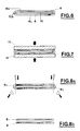
- the reel 4 thus formed comprises two elongated substantially rectilinear parallel side portions 4a at either side of the support 10, connected by curved portions of small radius at either end of the support 10. Once a reel 4 has been formed, the side portions 4a thereof are compressed (using known pressing means 11) against the stick-shaped support 10 (see Figure 7).
- the reel is sheared in the region of curved end portions 4b (for example see Figure 8a or, where the ends of the support 10 are rounded off, by a single cut along a plane lengthwise of the support to provide two bars with curved end portions which may be removed by cuts in the direction shown in Figure 8a) and, in this way, two capacitive rods 6 are created, both of which extend rectilinearly (see Figure 8b), the layers of film 1, 2 being flat. From the said rods, following the metallization of the longitudinal edge faces thereof 3 previously described, capacitors 9 are produced in the previously described way.
- a major feature of processes according to the invention is the creation of capacitive rods 6 extending rectilinearly, constituted by a stack of elongated pieces of films 1, 2 which are flat and arranged so as to alternate systematically. This simplifies subsequent compression and metallization phases for the rods since the surfaces thereof are flat instead of being curved as is the case with the previously known processes hereinbefore discussed.
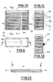
- Figures 9 and 10 show a frame 20 comprising a base 20a and two vertical C section walls 20b. Inside the frame 20 a plurality of reels 4 wound on corresponding stick-shaped supports 10 (in the manner previously described with reference to Figure 6) and a plurality of separation diaphragms 22, made either of metal or of synthetic resin, are placed alternately to form a stack 23. Each separation diaphragm 22 is interposed between two similar consecutive reels (see Figures 10, 11 and 12) with a flat side portion of each reel in contact with the adjacent diaphragm thus spacing the support from the diaphragm with edge faces of the reels formed by edges of the fi Ims wound round the support, exposed.
- the areas of the side faces of the stack are considerably greater than the section of the jet of the spraying means; this simplifies and, at the same time, speeds up the spraying phase thereby increasing the efficiency thereof.
- the sole area of each reel that it either not metallized or unsatisfactorily metallized is that of the curved ends 4b which, as will be explained below, are not used in the formation of the capacitive rods.
- thermal stabilization of the reels can be effected: this it done by subjecting the stack 23 to a predetermined temperature maintained for a predetermined period of time.
- the stack 23 is decompressed and the reels 4 are extracted from the frame 20 along with the corresponding diaphragms 22.
- the separation of the reels 4 one from the other is facilitated by the diaphragms 22 since these, after the brushing operation, constitute an interruption in the layer of metal sprayed on the edge faces of any two consecutively placed reels 4.
- the shearing of the ends 4b of each reel 4 creates at least two capacitive rods 6 each extending rectilinearly and in which the layers of film are flat, and the transverse shearing of these produces a plurality of individual capacitors 9.
- the supports (10) may be first removed from the reels (e.g by pushing using suitable apparatus, not shown), the metallization ensuring that the reels are sufficiently rigid and stable to retain their rectilinearform, the ends 4b then being sheared (see Figure 13).
- the individual capacitors 9 produced by a process embodying the invention are strictly in the form of parallelepipeds without any curvature (even very slight), and are thus clearly distinguished from the capacitors produced by the prior art processes involving so-called mother capacitors of arcuate form discussed above.
- the stack of superposed pieces of the films 1, 2 that constitutes each capacitor therefore has little or no tendency to peel and/or flake since no internal tension sufficient to cause this, exists.
Landscapes
- Engineering & Computer Science (AREA)
- Power Engineering (AREA)
- Manufacturing & Machinery (AREA)
- Microelectronics & Electronic Packaging (AREA)
- Fixed Capacitors And Capacitor Manufacturing Machines (AREA)
- Other Investigation Or Analysis Of Materials By Electrical Means (AREA)
Priority Applications (1)
| Application Number | Priority Date | Filing Date | Title |
|---|---|---|---|
| AT86300866T ATE49489T1 (de) | 1985-02-12 | 1986-02-10 | Herstellung von kondensatoren des stapeltyps. |
Applications Claiming Priority (4)
| Application Number | Priority Date | Filing Date | Title |
|---|---|---|---|
| IT333285 | 1985-02-12 | ||
| IT03332/85A IT1187312B (it) | 1985-02-12 | 1985-02-12 | Procedimento per la realizzazione di condensatori di tipo impilato |
| IT350385 | 1985-07-17 | ||
| IT03503/85A IT1186596B (it) | 1985-07-17 | 1985-07-17 | Procedimento per la realizzazione di condensatori di tipo impilato |
Publications (4)
| Publication Number | Publication Date |
|---|---|
| EP0194044A2 EP0194044A2 (en) | 1986-09-10 |
| EP0194044A3 EP0194044A3 (en) | 1987-09-30 |
| EP0194044B1 EP0194044B1 (en) | 1990-01-10 |
| EP0194044B2 true EP0194044B2 (en) | 1994-08-03 |
Family
ID=26325342
Family Applications (1)
| Application Number | Title | Priority Date | Filing Date |
|---|---|---|---|
| EP86300866A Expired - Lifetime EP0194044B2 (en) | 1985-02-12 | 1986-02-10 | Production of capacitors of the stacked type |
Country Status (10)
| Country | Link |
|---|---|
| US (1) | US4719675A (ja) |
| EP (1) | EP0194044B2 (ja) |
| JP (1) | JPH0611020B2 (ja) |
| BR (1) | BR8600803A (ja) |
| CA (1) | CA1260566A (ja) |
| DE (1) | DE3668255D1 (ja) |
| ES (1) | ES8801564A1 (ja) |
| FI (2) | FI860646A7 (ja) |
| IE (1) | IE57192B1 (ja) |
| PT (1) | PT82005B (ja) |
Families Citing this family (7)
| Publication number | Priority date | Publication date | Assignee | Title |
|---|---|---|---|---|
| US4942610A (en) * | 1989-03-31 | 1990-07-17 | Rayburn Charles C | Capacitive structure |
| EP0420162B1 (de) * | 1989-09-26 | 1995-05-03 | Siemens Aktiengesellschaft | Verfahren zum Herstellen eines elektrischen Leistungskondensators in Stapelbauweise |
| US5157820A (en) * | 1990-12-12 | 1992-10-27 | Integrated Power Components, Inc. | Capacitor manufacturing process |
| US5513424A (en) * | 1992-07-03 | 1996-05-07 | Compagnie Europeene De Composants Electroniques Lcc | Method for the manufacture of foil capacitors |
| KR100496488B1 (ko) * | 2002-09-18 | 2005-06-22 | 스마트전자 주식회사 | 적층형 필름 칩 커패시터의 제조방법 |
| JP2013074000A (ja) * | 2011-09-27 | 2013-04-22 | Kojima Press Industry Co Ltd | 積層フィルムコンデンサの製造方法 |
| JP6185051B2 (ja) * | 2013-05-01 | 2017-08-23 | 小島プレス工業株式会社 | フィルムコンデンサ及びフィルムコンデンサ素子並びにフィルムコンデンサ素子のエージング装置及びエージング方法 |
Family Cites Families (8)
| Publication number | Priority date | Publication date | Assignee | Title |
|---|---|---|---|---|
| US2654060A (en) * | 1950-01-20 | 1953-09-29 | Tinius Olsen Testing Mach Co | Capacity type strain gauge and method of manufacture |
| US2765517A (en) * | 1953-01-09 | 1956-10-09 | Western Electric Co | Method of making stacked type capacitors from metallized dielectric |
| US3471098A (en) * | 1968-01-10 | 1969-10-07 | Western Electric Co | Apparatus and method for winding tapes onto mandrels |
| US3728765A (en) * | 1969-06-18 | 1973-04-24 | Siemens Ag | Process for the production of capacitors |
| US3654532A (en) * | 1970-05-25 | 1972-04-04 | Illinois Tool Works | Multilayer plastic chip capacitor |
| DE2643087C2 (de) * | 1976-09-24 | 1978-08-24 | Siemens Ag, 1000 Berlin Und 8000 Muenchen | Verfahren zur Herstellung eines Schichtkondensators |
| US4531268A (en) * | 1981-02-27 | 1985-07-30 | Illinois Tool Works Inc. | Method of making capacitive structures |
| FR2528225A1 (fr) * | 1982-06-04 | 1983-12-09 | Europ Composants Electron | Procede de fabrication d'un pave elementaire de condensateur multi-couches et dispositif pour sa mise en oeuvre |
-
0
- FI FI860646A patent/FI860646L/fi unknown
-
1986
- 1986-02-03 IE IE299/86A patent/IE57192B1/en not_active IP Right Cessation
- 1986-02-07 BR BR8600803A patent/BR8600803A/pt not_active IP Right Cessation
- 1986-02-10 PT PT82005A patent/PT82005B/pt unknown
- 1986-02-10 EP EP86300866A patent/EP0194044B2/en not_active Expired - Lifetime
- 1986-02-10 DE DE8686300866T patent/DE3668255D1/de not_active Expired - Fee Related
- 1986-02-11 US US06/828,128 patent/US4719675A/en not_active Expired - Fee Related
- 1986-02-11 CA CA000501602A patent/CA1260566A/en not_active Expired
- 1986-02-12 ES ES552251A patent/ES8801564A1/es not_active Expired
- 1986-02-12 FI FI860646A patent/FI860646A7/fi not_active IP Right Cessation
- 1986-02-12 JP JP61028746A patent/JPH0611020B2/ja not_active Expired - Fee Related
Also Published As
| Publication number | Publication date |
|---|---|
| EP0194044A2 (en) | 1986-09-10 |
| JPS6271212A (ja) | 1987-04-01 |
| FI860646A0 (fi) | 1986-02-12 |
| IE860299L (en) | 1986-08-12 |
| DE3668255D1 (de) | 1990-02-15 |
| EP0194044B1 (en) | 1990-01-10 |
| FI860646A7 (fi) | 1986-08-18 |
| US4719675A (en) | 1988-01-19 |
| ES552251A0 (es) | 1987-11-01 |
| JPH0611020B2 (ja) | 1994-02-09 |
| IE57192B1 (en) | 1992-05-20 |
| EP0194044A3 (en) | 1987-09-30 |
| ES8801564A1 (es) | 1987-11-01 |
| PT82005A (en) | 1986-03-01 |
| FI860646L (fi) | 1986-08-13 |
| CA1260566A (en) | 1989-09-26 |
| BR8600803A (pt) | 1986-11-04 |
| PT82005B (pt) | 1991-03-20 |
Similar Documents
| Publication | Publication Date | Title |
|---|---|---|
| EP0194044B2 (en) | Production of capacitors of the stacked type | |
| HU203817B (en) | Electric capacitor made from undeformably fixed coil or sheet pack containing metallized plastic sheet arranged in layer | |
| GB1216946A (en) | Improvements in or relating to methods of manufacturing electrical capacitors | |
| BR8405941A (pt) | Capacitor eletrico construido a partir de um empilhamento reforcado de camadas dieletricas metalizadas,justapostas,e processo para a sua fabricacao | |
| CA1241392A (en) | Electrical capacitor and method for the manufacture thereof | |
| ES8202981A1 (es) | Procedimiento para la fabricacion de condensadores en capas | |
| JPH0275429A (ja) | 雄型コネクタ用端子の製造方法 | |
| FR2548440A1 (fr) | Film metallise pour la realisation de condensateurs et procede de fabrication desdits condensateurs | |
| JPH0227554Y2 (ja) | ||
| JPH0793237B2 (ja) | フィルムコンデンサの製造方法 | |
| US5518567A (en) | Process for the production of a composite material part constituted by a central body and ailerons | |
| JPH0464211A (ja) | 金属化フィルムコンデンサの製造方法 | |
| JPH0232780B2 (ja) | ||
| CN2566431Y (zh) | 电容器 | |
| JPH02907Y2 (ja) | ||
| JPH0357205A (ja) | 積層フィルムコンデンサの製造方法 | |
| JPH0464210A (ja) | 金属化フィルムコンデンサの製造方法 | |
| JPS59228712A (ja) | コンデンサの製造方法 | |
| JPS59103324A (ja) | コンデンサ用金属蒸着フイルムの非蒸着部形成方法及び装置 | |
| JPH02198121A (ja) | フィルムコンデンサの製造方法 | |
| JPH11168025A (ja) | フィルムコンデンサの製造方法 | |
| JPH048935B2 (ja) | ||
| KR960012290B1 (ko) | 적층필름콘덴서의 제조방법 | |
| JPH0793239B2 (ja) | 金属化プラスチックフィルムコンデンサの製造方法 | |
| JPS59208817A (ja) | コンデンサ |
Legal Events
| Date | Code | Title | Description |
|---|---|---|---|
| PUAI | Public reference made under article 153(3) epc to a published international application that has entered the european phase |
Free format text: ORIGINAL CODE: 0009012 |
|
| AK | Designated contracting states |
Kind code of ref document: A2 Designated state(s): AT BE CH DE FR GB IT LI LU NL SE |
|
| PUAL | Search report despatched |
Free format text: ORIGINAL CODE: 0009013 |
|
| AK | Designated contracting states |
Kind code of ref document: A3 Designated state(s): AT BE CH DE FR GB IT LI LU NL SE |
|
| 17P | Request for examination filed |
Effective date: 19871014 |
|
| 17Q | First examination report despatched |
Effective date: 19890302 |
|
| GRAA | (expected) grant |
Free format text: ORIGINAL CODE: 0009210 |
|
| AK | Designated contracting states |
Kind code of ref document: B1 Designated state(s): AT BE CH DE FR GB IT LI LU NL SE |
|
| REF | Corresponds to: |
Ref document number: 49489 Country of ref document: AT Date of ref document: 19900115 Kind code of ref document: T |
|
| REF | Corresponds to: |
Ref document number: 3668255 Country of ref document: DE Date of ref document: 19900215 |
|
| ITTA | It: last paid annual fee | ||
| ET | Fr: translation filed | ||
| ITF | It: translation for a ep patent filed | ||
| PLBI | Opposition filed |
Free format text: ORIGINAL CODE: 0009260 |
|
| 26 | Opposition filed |
Opponent name: SIEMENS AKTIENGESELLSCHAFT, BERLIN UND MUENCHEN Effective date: 19900926 |
|
| NLR1 | Nl: opposition has been filed with the epo |
Opponent name: SIEMENS AG. |
|
| EPTA | Lu: last paid annual fee | ||
| PUAH | Patent maintained in amended form |
Free format text: ORIGINAL CODE: 0009272 |
|
| STAA | Information on the status of an ep patent application or granted ep patent |
Free format text: STATUS: PATENT MAINTAINED AS AMENDED |
|
| 27A | Patent maintained in amended form |
Effective date: 19940803 |
|
| AK | Designated contracting states |
Kind code of ref document: B2 Designated state(s): AT BE CH DE FR GB IT LI LU NL SE |
|
| REG | Reference to a national code |
Ref country code: CH Ref legal event code: AEN |
|
| ET3 | Fr: translation filed ** decision concerning opposition | ||
| NLR2 | Nl: decision of opposition | ||
| ITPR | It: changes in ownership of a european patent |
Owner name: ASSUNZIONE O VARIAZIONE MANDATO;MODIANO & ASSOCIAT |
|
| NLR3 | Nl: receipt of modified translations in the netherlands language after an opposition procedure | ||
| EAL | Se: european patent in force in sweden |
Ref document number: 86300866.0 |
|
| REG | Reference to a national code |
Ref country code: GB Ref legal event code: IF02 |
|
| PGFP | Annual fee paid to national office [announced via postgrant information from national office to epo] |
Ref country code: FR Payment date: 20040129 Year of fee payment: 19 |
|
| PGFP | Annual fee paid to national office [announced via postgrant information from national office to epo] |
Ref country code: SE Payment date: 20040130 Year of fee payment: 19 Ref country code: LU Payment date: 20040130 Year of fee payment: 19 |
|
| PGFP | Annual fee paid to national office [announced via postgrant information from national office to epo] |
Ref country code: GB Payment date: 20040204 Year of fee payment: 19 |
|
| PGFP | Annual fee paid to national office [announced via postgrant information from national office to epo] |
Ref country code: BE Payment date: 20040205 Year of fee payment: 19 |
|
| PGFP | Annual fee paid to national office [announced via postgrant information from national office to epo] |
Ref country code: AT Payment date: 20040211 Year of fee payment: 19 |
|
| PGFP | Annual fee paid to national office [announced via postgrant information from national office to epo] |
Ref country code: CH Payment date: 20040217 Year of fee payment: 19 |
|
| PGFP | Annual fee paid to national office [announced via postgrant information from national office to epo] |
Ref country code: NL Payment date: 20040223 Year of fee payment: 19 |
|
| PGFP | Annual fee paid to national office [announced via postgrant information from national office to epo] |
Ref country code: DE Payment date: 20040423 Year of fee payment: 19 |
|
| PG25 | Lapsed in a contracting state [announced via postgrant information from national office to epo] |
Ref country code: IT Free format text: LAPSE BECAUSE OF NON-PAYMENT OF DUE FEES Effective date: 20050210 Ref country code: GB Free format text: LAPSE BECAUSE OF NON-PAYMENT OF DUE FEES Effective date: 20050210 Ref country code: AT Free format text: LAPSE BECAUSE OF NON-PAYMENT OF DUE FEES Effective date: 20050210 |
|
| PG25 | Lapsed in a contracting state [announced via postgrant information from national office to epo] |
Ref country code: SE Free format text: LAPSE BECAUSE OF NON-PAYMENT OF DUE FEES Effective date: 20050211 |
|
| PG25 | Lapsed in a contracting state [announced via postgrant information from national office to epo] |
Ref country code: LI Free format text: LAPSE BECAUSE OF NON-PAYMENT OF DUE FEES Effective date: 20050228 Ref country code: CH Free format text: LAPSE BECAUSE OF NON-PAYMENT OF DUE FEES Effective date: 20050228 Ref country code: BE Free format text: LAPSE BECAUSE OF NON-PAYMENT OF DUE FEES Effective date: 20050228 |
|
| BERE | Be: lapsed |
Owner name: *ARCOTRONICS ITALIA S.P.A. Effective date: 20050228 |
|
| PG25 | Lapsed in a contracting state [announced via postgrant information from national office to epo] |
Ref country code: NL Free format text: LAPSE BECAUSE OF NON-PAYMENT OF DUE FEES Effective date: 20050901 Ref country code: DE Free format text: LAPSE BECAUSE OF NON-PAYMENT OF DUE FEES Effective date: 20050901 |
|
| GBPC | Gb: european patent ceased through non-payment of renewal fee |
Effective date: 20050206 |
|
| EUG | Se: european patent has lapsed | ||
| REG | Reference to a national code |
Ref country code: CH Ref legal event code: PL |
|
| PG25 | Lapsed in a contracting state [announced via postgrant information from national office to epo] |
Ref country code: FR Free format text: LAPSE BECAUSE OF NON-PAYMENT OF DUE FEES Effective date: 20051031 |
|
| NLV4 | Nl: lapsed or anulled due to non-payment of the annual fee |
Effective date: 20050901 |
|
| REG | Reference to a national code |
Ref country code: FR Ref legal event code: ST Effective date: 20051031 |
|
| BERE | Be: lapsed |
Owner name: *ARCOTRONICS ITALIA S.P.A. Effective date: 20050228 |