EP0189680A2 - Appareil de stabilisation de source d'alimentation - Google Patents
Appareil de stabilisation de source d'alimentation Download PDFInfo
- Publication number
- EP0189680A2 EP0189680A2 EP85309536A EP85309536A EP0189680A2 EP 0189680 A2 EP0189680 A2 EP 0189680A2 EP 85309536 A EP85309536 A EP 85309536A EP 85309536 A EP85309536 A EP 85309536A EP 0189680 A2 EP0189680 A2 EP 0189680A2
- Authority
- EP
- European Patent Office
- Prior art keywords
- voltage
- secondary coil
- power source
- source apparatus
- coil
- Prior art date
- Legal status (The legal status is an assumption and is not a legal conclusion. Google has not performed a legal analysis and makes no representation as to the accuracy of the status listed.)
- Granted
Links
Images
Classifications
-
- H—ELECTRICITY
- H02—GENERATION; CONVERSION OR DISTRIBUTION OF ELECTRIC POWER
- H02M—APPARATUS FOR CONVERSION BETWEEN AC AND AC, BETWEEN AC AND DC, OR BETWEEN DC AND DC, AND FOR USE WITH MAINS OR SIMILAR POWER SUPPLY SYSTEMS; CONVERSION OF DC OR AC INPUT POWER INTO SURGE OUTPUT POWER; CONTROL OR REGULATION THEREOF
- H02M3/00—Conversion of DC power input into DC power output
- H02M3/22—Conversion of DC power input into DC power output with intermediate conversion into AC
- H02M3/24—Conversion of DC power input into DC power output with intermediate conversion into AC by static converters
- H02M3/28—Conversion of DC power input into DC power output with intermediate conversion into AC by static converters using discharge tubes with control electrode or semiconductor devices with control electrode to produce the intermediate AC
- H02M3/325—Conversion of DC power input into DC power output with intermediate conversion into AC by static converters using discharge tubes with control electrode or semiconductor devices with control electrode to produce the intermediate AC using devices of a triode or a transistor type requiring continuous application of a control signal
- H02M3/335—Conversion of DC power input into DC power output with intermediate conversion into AC by static converters using discharge tubes with control electrode or semiconductor devices with control electrode to produce the intermediate AC using devices of a triode or a transistor type requiring continuous application of a control signal using semiconductor devices only
- H02M3/338—Conversion of DC power input into DC power output with intermediate conversion into AC by static converters using discharge tubes with control electrode or semiconductor devices with control electrode to produce the intermediate AC using devices of a triode or a transistor type requiring continuous application of a control signal using semiconductor devices only in a self-oscillating arrangement
- H02M3/3385—Conversion of DC power input into DC power output with intermediate conversion into AC by static converters using discharge tubes with control electrode or semiconductor devices with control electrode to produce the intermediate AC using devices of a triode or a transistor type requiring continuous application of a control signal using semiconductor devices only in a self-oscillating arrangement with automatic control of output voltage or current
- H02M3/3387—Conversion of DC power input into DC power output with intermediate conversion into AC by static converters using discharge tubes with control electrode or semiconductor devices with control electrode to produce the intermediate AC using devices of a triode or a transistor type requiring continuous application of a control signal using semiconductor devices only in a self-oscillating arrangement with automatic control of output voltage or current in a push-pull configuration
- H02M3/3388—Conversion of DC power input into DC power output with intermediate conversion into AC by static converters using discharge tubes with control electrode or semiconductor devices with control electrode to produce the intermediate AC using devices of a triode or a transistor type requiring continuous application of a control signal using semiconductor devices only in a self-oscillating arrangement with automatic control of output voltage or current in a push-pull configuration of the parallel type
-
- H—ELECTRICITY
- H02—GENERATION; CONVERSION OR DISTRIBUTION OF ELECTRIC POWER
- H02M—APPARATUS FOR CONVERSION BETWEEN AC AND AC, BETWEEN AC AND DC, OR BETWEEN DC AND DC, AND FOR USE WITH MAINS OR SIMILAR POWER SUPPLY SYSTEMS; CONVERSION OF DC OR AC INPUT POWER INTO SURGE OUTPUT POWER; CONTROL OR REGULATION THEREOF
- H02M3/00—Conversion of DC power input into DC power output
- H02M3/22—Conversion of DC power input into DC power output with intermediate conversion into AC
- H02M3/24—Conversion of DC power input into DC power output with intermediate conversion into AC by static converters
- H02M3/28—Conversion of DC power input into DC power output with intermediate conversion into AC by static converters using discharge tubes with control electrode or semiconductor devices with control electrode to produce the intermediate AC
- H02M3/325—Conversion of DC power input into DC power output with intermediate conversion into AC by static converters using discharge tubes with control electrode or semiconductor devices with control electrode to produce the intermediate AC using devices of a triode or a transistor type requiring continuous application of a control signal
- H02M3/335—Conversion of DC power input into DC power output with intermediate conversion into AC by static converters using discharge tubes with control electrode or semiconductor devices with control electrode to produce the intermediate AC using devices of a triode or a transistor type requiring continuous application of a control signal using semiconductor devices only
- H02M3/33561—Conversion of DC power input into DC power output with intermediate conversion into AC by static converters using discharge tubes with control electrode or semiconductor devices with control electrode to produce the intermediate AC using devices of a triode or a transistor type requiring continuous application of a control signal using semiconductor devices only having more than one ouput with independent control
Definitions
- the present invention relates to a multiple output type stabilizing power source apparatus for generating stabilized AC and DC voltages.
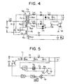
- a typical conventional multiple output type stabilizing power source apparatus as shown in Fig. 5 supplies a stabilized DC voltage to a DC load such as electronic equipment and a stabilized AC voltage to an AC load such as a fluorescent lamp.
- the stabilizing power source apparatus has inverters at the primary and secondary winding sides.
- a reference symbol V 0 denotes a DC voltage; Q 1 , a switching transistor; and T 1 , an inverter transformer.
- the inverter transformer T 1 has a primary winding Np and a secondary winding N s .
- Reference symbols D 1 and D 2 denote rectifying diodes, respectively; L 1 , a choke coil; and C 1 , a smoothing capacitor.
- a reference symbol A 1 denotes a differential amplifier for comparing a reference voltage V R with a DC output V 1 from the secondary winding N S and generating a signal corresponding to the difference.
- a reference symbol OSC denotes an oscillator for generating a triangular wave signal; and PWM, a pulse width modulator for converting the triangular wave from the oscillator OSC to pulses of the same frequency as that of the triangular wave and for changing a pulse width of the converted pulses in accordance with a shift of a crossing point between the triangular wave from the oscillator OSC and the signal from the differential amplifier A 1 .
- a reference symbol DR denotes a driver for amplifying the pulses from the pulse width modulator PWM and for supplying an amplified signal to the base of the transistor Q 1 .
- a reference symbol INV denotes an inverter for receiving the DC voltage V 1 from the secondary winding N S and for generating an AC voltage upon switching; T 2 , a voltage transformer for transforming the AC voltage from the inverter INV; C F , a waveshaping capacitor; and R L , an AC load for receiving an AC output V 2 .
- a resistor R S detects a current flowing through the AC load R L , and the inverter INV is switched to keep the current constant in response to the detection signal.
- a rectangular wave current obtained upon switching of the transistor Q 1 is rectified by the diodes D 1 and D 2 connected to the secondary winding N S .
- the rectified current is smoothed by the choke coil L 1 and the capacitor C 1 to provide the DC output V 1 .
- the DC output V 1 is supplied to the differential amplifier A 1 and is compared with the reference input voltage V R .
- the differential amplifier A 1 provides a signal corresponding to the difference to the pulse width modulator PWM.
- the pulse width modulator PWM the triangular wave from the oscillator OSC is converted to the pulses of the same frequency as that of the triangular wave.
- the pulse width is varied in accordance with the crossing point between the leading ramp of the triangular wave and the output from the differential amplifier A I .
- the pulse is amplified by the driver DR, and the amplified pulse is supplied to the base of the transistor Q 1 .
- the duty factor of the transistor Q 1 is thus controlled in response to the output from the differential amplifier A 1 . Therefore, the DC voltage V 1 is kept constant.
- the stabilized DC output V 1 is supplied to the inverter INV and is converted to the AC voltage upon its switching.
- the AC voltage is boosted by the transformer T 2 .
- the boosted voltage is then smoothed by the capacitor C F , and the smoothed output is supplied to the AC load R L .
- a stabilizing power source apparatus having a primary coil for receiving a DC voltage, a secondary coil magnetically coupled to the primary coil, and a switching element connected in series with the primary coil, the switching element being operated to turn on/off a current flowing through the primary coil so as to obtain a desired voltage output at the secondary coil, wherein the secondary coil is constituted by a first secondary coil and a second secondary coil, and the switching element is provided with a control input terminal for controlling switching thereof, and the apparatus comprises:
- a stabilizing power source apparatus having a first primary coil for receiving a DC voltage, a secondary coil magnetically coupled to the first primary coil, and a first switching element connected in series with the first primary coil, the first switching element being operated to turn on/off a current flowing through the first primary coil so as to obtain a desired voltage output at the secondary coil, wherein the first switching element has a control input terminal for controlling switching thereof, the secondary coil has at least first and second secondary coils, and the apparatus comprises:
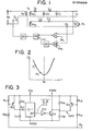
- Fig. 1 is a circuit diagram of a stabilizing power source apparatus according to an embodiment of the present invention.
- the same reference numerals as in Fig. 5 denote the same parts in Fig. 1.
- a reference symbol V 0 denotes an input DC voltage
- Q 1 a switching element
- T 3 an inverter transformer.
- the inverter transformer T 3 has a primary winding Np, a DC voltage output secondary winding N S1 magnetically coupled to the primary winding Np, and an AC output secondary winding N S2 magnetically coupled to the primary winding Np.
- the switching element Q 1 comprises a bipolar transistor but can be replaced with a GTO thyristor, a normal thyristor or the like.
- Reference symbols D 1 and D 2 denote rectifying diodes for the secondary winding N S1 ; L 1 , a choke coil; C 1 , a smoothing capacitor; L 2 , a choke coil for the secondary winding NS2 ; C 3 , a filter capacitor; R S , a resistor for detecting a load current; and R L , an AC load.
- a reference symbol A 1 denotes a differential amplifier for comparing a reference input voltage V R1 with the DC voltage from the secondary winding N S1 and generating a signal representing the difference therebetween.
- a reference symbol A 2 denotes a differential amplifier for receiving the AC voltage from the load current detecting resistor R S inserted between the secondary winding N S2 and the load R L , comparing the AC voltage with a reference input voltage V R2 and generating a signal representing the difference therebetween.
- a reference symbol OSC' denotes an oscillator for generating a triangular wave, the leading ramp of which is changed in response to the signal from the differential amplifier A 2 .
- a reference symbol PM denotes a pulse modulator for comparing the output signal from the differential amplifier A 1 with the triangular wave from the oscillator OSC' and generating a pulse, the width and frequency of which are changed in accordance with the shift of the crossing point between these input signals.
- a reference symbol DR denotes a driver for amplifying the pulse and supplying an amplified signal to the base of the transistor Q 1 .
- the duty factor of the transistor Q 1 is controlled to keep the DC output voltage V 1 constant.
- the switching frequency of the transistor Q 1 is controlled to keep the AC load current constant.
- Fig. 2 is a graph showing the relationship between input impedance Z and frequency f when the AC load R L is viewed from the secondary winding N S2 .
- the switching frequency f of the transistor Q 1 is decreased. Accordingly, the input impedance Z is increased and the load current is decreased (P 1 in Fig. 2).
- the switching frequency f of the transistor Q 1 is increased. Accordingly, the input impedance Z is increased, and the load current is also increased (P 2 in Fig. 2).
- the input impedance Z is given by:
- the resonant frequency f D is given by:
- Fig. 3 is a circuit diagram of the oscillator OSC' in the apparatus in Fig. 1.
- reference symbols R 11 to R 17 denote resistors; C 11 and C 12 , capacitors; Q 11 to Q 13' transistors; IC1, an integrated circuit element as a timer circuit; and IC 2 , an integrated circuit element as a NAND gate.
- the timer circuit IC 1 generates a clock signal with a period T at an output terminal OUT thereof so as to charge the capacitor C 11 in accordance with a time constant determined by the resistance of the resistor R 15 and the capacitance of the capacitor C 11 , and at the same time, discharge the capacitor C 11 in accordance with a time constant determined by the resistance of the resistor R17 and the capacitance of the capacitor C 11 .
- the clock signal is supplied to the base of the transistor Q 13 through the NAND gate IC 2 , so that the triangular wave voltage appears across the capacitor C 12 upon ON/OFF operation of the transistor Q 13'
- the triangular wave voltage signal is supplied from the collector of the transistor Q 13 to the pulse modulator PM.
- the transistor Q 11 When the AC voltage V 2 is constant and the signal from the differential amplifier A 2 is the reference voltage value, the transistor Q 11 is turned off.
- the timer circuit IC 1 generates the clock signal of a predetermined frequency.
- the internal resistance of the transistor Q 11 is decreased and the charge rate of the capacitor C 11 is increased. As a result, the period T of the clock signal is shortened.
- the internal resistance of the transistor Q 12 is decreased to increase the charge rate of the capacitor C 12 .
- the leading ramp of the triangular wave becomes steep. However, when the AC output V 2 is increased, the leading ramp of the triangular wave becomes moderate in the reverse process.
- the frequency of the oscillator OSC' varies in accordance with variations in the output signal from the differential amplifier A 2 which, in turn, varies in accordance with variations in that AC output V 2 0
- the width and frequency of the pulse supplied to the base of the switching transistor Q 1 vary in accordance with the variations in the voltage from the differential amplifier A. and the frequency of the triangular wave from the oscillator OSC'.
- the duty factor and the switching frequency of the transistor Q 1 are controlled to keep the DC voltage V 1 and the AC voltage V 2 constant.
- the inverter at the primary winding comprises a forward type inverter.
- the present invention is not limited to this arrangement.
- a half-bridge type inverter or a full-bridge type inverter can be used in place of the forward type inverter.
- the pulse width and frequency control circuit is exemplified by a PUM consisting of a variable frequency triangular wave oscillator and a comparator in the above description.
- the output signals from the two amplifiers can be supplied to an astable multivibrator to control the ON time intervals of transistors constituting the astable multivibrator. Therefore, the switching frequency and the ON time intervals can be simultaneously controlled.
- Fig. 4 is a circuit diagram of a stabilizing power source apparatus according to another embodiment of the present invention.
- the same reference numerals as in Fig. 1 denote the same parts in Fig. 4.
- a reference numeral V 0 denotes an input DC voltage
- L p a choke coil
- Q 2 and Q 3 switching transistors which are alternately turned on/off
- T 1 an inverter transformer.
- the inverter transformer T 1 has primary windings Np 1 and Np 2 .
- a reference symbol N D denotes a drive coil connected to the bases of the transistors Q 2 and Q 3 .
- a reference symbol Cp denotes a resonant capacitor inserted in parallel with the primary windings Np I and Np 2 .
- the switching transistors Q 2 and Q 3 comprise bipolar transistors, respectively, in the above arrangement, but can be replaced with other switching elements such as MOSFETs, GTO thyristors, normal thyristors.
- a waveshaper When thyristors are used, a waveshaper must be inserted between the coil N D and the two terminals of the switching element. In the case of thyristors, a commutating circuit must be added to turn off the thyristors.
- the above arrangement constitutes a resonant inverter for generating a sinusoidal wave voltage across the primary windings Np 1 and Np 2 .
- the switching operation of the two transistors is called push-pull operation.
- N S1 and N S2 denote secondary windings of the inverter transformer T 1 ; L S1 and L S2' saturable reactors connected in series with the secondary windings N S1 and NS2, respectively; D 1 , D 2 and D 3 , rectifying diodes; L 1 , a choke coil; and C 1 , a smoothing capacitor.
- N S3 denotes an AC output secondary winding
- C F a waveshaping capacitor
- R L an AC load
- a reference symbol A 1 denotes a differential amplifier for comparing a reference voltage V R with the DC voltage V 1 and generating a signal representing the difference therebetween.
- a reference symbol Q 4 denotes a transistor, the base of which is connected to the differential amplifier A. to receive the difference signal as a base current, the collector of which is connected to reactors L S1 and L S1 respectively through the saturable diodes D 4 and D 5 and the emitter of which is connected to the DC voltage V 1 .
- the transistor Q 4 comprises a bipolar transistor, but can be replaced' with another output current control element such as a MOSFFT.
- a voltage obtained by dividing the DC input voltage V 0 in accordance with the number of turns is induced at the drive coil N D magnetically coupled to the primary winding Np l .
- the base-emitter path of the transistor Q 3 is reverse-biased, and the transistor Q 3 is kept off.
- the voltage generated at the primary winding N P1 is a sinusoidal wave.
- a self-excited angular frequency w is given as: where L H is the inductance of the primary winding N P1 of the inverter transformer T 1 , C P ' is the capacitance for the primary winding N P1 based on the resonant capacitor Cp, and C F ' is the capacitance for the primary winding N P1 based on the waveshaping capacitor C F .
- the induction voltage at the drive coil N D which has been supplied as the reverse-bias voltage to the base of the transistor Q 3 is then forward-biased.
- the transistor Q 2 is now reverse-biased to turn on the transistor Q 3 and turn off the transistor Q 2 .
- the self-excited resonance is set in the negative half cycle.
- the transistors Q 2 and Q 3 are alternately turned on/off to generate the sinusoidal wave current at the primary windings N p1 and Np 2 .
- the current is then extracted at the secondary windings N S1 and N S2'
- the sinusoidal wave current is full-wave rectified by the diodes D 1 and D 3 .
- the rectified current is smoothed by the choke coil L 1 and the capacitor C 1 to provide the DC voltage V 1 .
- the DC voltage V 1 still varies in accordance with variations in the input DC voltage V 0 .
- the saturable reactors L S1 and L S2 are connected in series with the secondary windings N S1 and N S2 , respectively, thereby performing phase control.
- the saturable reactors are used to reduce noise at the secondary windings of the transformer.
- the saturable reactors serve as elements for controlling ON time of currents flowing through the coils and may be replaced with switching elements such as transistors.
- the saturable reactors L S1 and L S2 are arranged such that the phase control angles representing the present saturation timings are determined by the reset values of the magnetic flux. When the reset values are increased, the phase control angles are increased, and thus the output voltages are decreased.
- the DC voltage V 1 is compared by the differential amplifier A 1 with the reference input voltage V R , and the difference signal from the differential amplifier A 1 is supplied to the base of the transistor Q 4 .
- the collector of the transistor Q 4 is connected to the saturable reactors L S1 and LS2, the reset values of the saturable reactors L S1 and L S2 are controlled to cancel the variations in the DC voltage V 1 .
- the DC voltage V 1 is kept constant.
- the AC voltage from the secondary windings N S3 is supplied to the AC load R L through the waveshaping capacitor C F .
- the transistors Q 2 and Q 3 have conduction times.
- the transistors Q 2 and Q 3 are simultaneously turned on when the sinusoidal wave voltages at the primary windings N P1 and N p 2 are set to 0.
- the choke coil Lp is arranged at the DC input side to limit the short-circuiting current.
- the capacitor C F is used as the waveshaping element of the AC output secondary winding N S3 .
- a choke coil may be inserted in place of the capacitor C F .
- the self-excited angular frequency w' is given as: where L F ' is the inductance of the choke coil L F which is figured out on the basis of the primary winding N P1 , and Lp//L F ' is the total inductance of the inductance of the choke coil Lp and the inductance L F '.
- the sinusoidal wave voltage is applied in the collector-emitter paths of the transistors Q 2 and Q 3 , and the voltages at the transistors Q 2 and Q 3 are substantially zero at the turn on/off timing, thereby decreasing the switching loss.
- the line filter at the input side need not be large in size.
- the switching loss is decreased as described above, the switching frequency can be increased, and the inverter transformer T 1 can be made compact.
- the stabilizing power source apparatus has a single switching circuit, so that the number of components is decreased and the manufacturing cost is decreased.
- the apparatus is made small as a whole, and its reliability is improved.
- the sinusoidal wave is supplied to the primary windings, so that the conduction noise is decreased, and the circuit arrangement can be simplified.
- the transformer can be made compact and the apparatus as a whole can be made compact.
- the number of transformers can be decreased, and the insulated portion between the primary and secondary windings is decreased, thereby simplifying insulation design.
Landscapes
- Engineering & Computer Science (AREA)
- Power Engineering (AREA)
- Dc-Dc Converters (AREA)
- Inverter Devices (AREA)
Priority Applications (1)
| Application Number | Priority Date | Filing Date | Title |
|---|---|---|---|
| EP91202705A EP0471421B1 (fr) | 1984-12-28 | 1985-12-30 | Appareil de source de puissance stabilisante |
Applications Claiming Priority (4)
| Application Number | Priority Date | Filing Date | Title |
|---|---|---|---|
| JP277717/84 | 1984-12-28 | ||
| JP27771784A JPS61157263A (ja) | 1984-12-28 | 1984-12-28 | 安定化電源装置 |
| JP280922/84 | 1984-12-29 | ||
| JP28092284A JPS61161964A (ja) | 1984-12-29 | 1984-12-29 | 安定化電源装置 |
Related Child Applications (1)
| Application Number | Title | Priority Date | Filing Date |
|---|---|---|---|
| EP91202705.9 Division-Into | 1991-10-18 |
Publications (3)
| Publication Number | Publication Date |
|---|---|
| EP0189680A2 true EP0189680A2 (fr) | 1986-08-06 |
| EP0189680A3 EP0189680A3 (en) | 1988-03-16 |
| EP0189680B1 EP0189680B1 (fr) | 1993-02-10 |
Family
ID=26552531
Family Applications (2)
| Application Number | Title | Priority Date | Filing Date |
|---|---|---|---|
| EP91202705A Expired - Lifetime EP0471421B1 (fr) | 1984-12-28 | 1985-12-30 | Appareil de source de puissance stabilisante |
| EP85309536A Expired - Lifetime EP0189680B1 (fr) | 1984-12-28 | 1985-12-30 | Appareil de stabilisation de source d'alimentation |
Family Applications Before (1)
| Application Number | Title | Priority Date | Filing Date |
|---|---|---|---|
| EP91202705A Expired - Lifetime EP0471421B1 (fr) | 1984-12-28 | 1985-12-30 | Appareil de source de puissance stabilisante |
Country Status (3)
| Country | Link |
|---|---|
| US (1) | US4677534A (fr) |
| EP (2) | EP0471421B1 (fr) |
| DE (2) | DE3587090T2 (fr) |
Cited By (6)
| Publication number | Priority date | Publication date | Assignee | Title |
|---|---|---|---|---|
| EP0240312A3 (en) * | 1986-03-31 | 1989-07-26 | Kabushiki Kaisha Toshiba | Stabilized electric power apparatus for generating direct and alternating current simultaneously in one transformer |
| EP0355415A3 (en) * | 1988-08-26 | 1990-08-16 | Ant Nachrichtentechnik Gmbh | Switching regulator |
| EP0498651A3 (en) * | 1991-02-08 | 1992-10-14 | General Electric Company | High power factor power supply |
| EP0564413A3 (en) * | 1992-02-28 | 1995-08-23 | Canon Kk | Image forming apparatus copying with power supply voltage drift |
| WO2009070086A1 (fr) * | 2007-11-27 | 2009-06-04 | Milux Holding Sa | Regulation de transfert d'energie pour systeme de dispositif medical |
| EP2200164A4 (fr) * | 2007-09-26 | 2010-09-22 | Huawei Tech Co Ltd | Dispositif d'alimentation de convertisseur de courant continu et procédé pour améliorer un tel dispositif |
Families Citing this family (57)
| Publication number | Priority date | Publication date | Assignee | Title |
|---|---|---|---|---|
| US4772995A (en) * | 1987-01-08 | 1988-09-20 | Veeco Instruments Inc. | Switching supply with pulse width and rate modulation |
| US4855885A (en) * | 1988-04-11 | 1989-08-08 | Dsl Dynamic Sciences Limited | Light beam intensifier |
| US4893227A (en) * | 1988-07-08 | 1990-01-09 | Venus Scientific, Inc. | Push pull resonant flyback switchmode power supply converter |
| CA1316980C (fr) * | 1988-12-27 | 1993-04-27 | Daniel C. Hughey | Bloc d'alimentation |
| US5128593A (en) * | 1990-01-25 | 1992-07-07 | Beckman Instruments, Inc. | Power supply for gas-filled lamps |
| US5448469A (en) * | 1990-02-15 | 1995-09-05 | Deutsche Thomson-Brandt Gmbh | Switch mode power supply with output feedback isolation |
| US5231563A (en) * | 1990-09-07 | 1993-07-27 | Itt Corporation | Square wave converter having an improved zero voltage switching operation |
| US5126931A (en) * | 1990-09-07 | 1992-06-30 | Itt Corporation | Fixed frequency single ended forward converter switching at zero voltage |
| US5084666A (en) * | 1990-10-23 | 1992-01-28 | International Business Machines Corporation | Switchable output voltage converter |
| US5132889A (en) * | 1991-05-15 | 1992-07-21 | Ibm Corporation | Resonant-transition DC-to-DC converter |
| US5285367A (en) * | 1992-02-07 | 1994-02-08 | Power Integrations, Inc. | Linear load circuit to control switching power supplies under minimum load conditions |
| GB9214896D0 (en) * | 1992-07-14 | 1992-08-26 | Attwood Brian E | A low cost 1mhz ferrite regulated converter |
| US5479087A (en) * | 1992-10-02 | 1995-12-26 | Compaq Computer Corp. | Synchronized switch tapped coupled inductor regulation circuit |
| WO1994022208A1 (fr) * | 1993-03-17 | 1994-09-29 | National Semiconductor Corporation | Circuit a deplacement de frequence pour regulateur a decoupage |
| JP2758552B2 (ja) * | 1993-08-27 | 1998-05-28 | 浜松ホトニクス株式会社 | プッシュプル共振型スイッチング電源回路 |
| US5640315A (en) * | 1994-03-18 | 1997-06-17 | Nippon Steel Corporation | Switching regulator |
| DE4424800A1 (de) * | 1994-07-14 | 1996-01-18 | Philips Patentverwaltung | Schaltungsanordnung zum Liefern von Speisespannungen |
| KR0150384B1 (ko) * | 1995-05-31 | 1998-10-15 | 배순훈 | 고압안정화회로 |
| US5690693A (en) * | 1995-06-07 | 1997-11-25 | Sulzer Intermedics Inc. | Transcutaneous energy transmission circuit for implantable medical device |
| US5702431A (en) * | 1995-06-07 | 1997-12-30 | Sulzer Intermedics Inc. | Enhanced transcutaneous recharging system for battery powered implantable medical device |
| US5745358A (en) * | 1996-05-01 | 1998-04-28 | Compaq Computer Corporation | Variable-frequency converter with constant programmed delay |
| US5973939A (en) * | 1996-08-29 | 1999-10-26 | Trw Inc. | Double forward converter with soft-PWM switching |
| AU722043B2 (en) | 1997-01-24 | 2000-07-20 | Synqor, Inc. | High efficiency power converter |
| US7269034B2 (en) | 1997-01-24 | 2007-09-11 | Synqor, Inc. | High efficiency power converter |
| US6130509A (en) * | 1999-01-22 | 2000-10-10 | Dell Computer Corporation | Balanced feedback system for floating cold cathode fluorescent lamps |
| US6461292B1 (en) | 1999-08-12 | 2002-10-08 | Obtech Medical Ag | Anal incontinence treatment with wireless energy supply |
| US6482145B1 (en) | 2000-02-14 | 2002-11-19 | Obtech Medical Ag | Hydraulic anal incontinence treatment |
| US6464628B1 (en) | 1999-08-12 | 2002-10-15 | Obtech Medical Ag | Mechanical anal incontinence |
| US6471635B1 (en) | 2000-02-10 | 2002-10-29 | Obtech Medical Ag | Anal incontinence disease treatment with controlled wireless energy supply |
| ATE306233T1 (de) * | 2000-02-10 | 2005-10-15 | Potencia Medical Ag | Behandlung der harninkontinenz mit kabelloser energiezufuhr |
| MXPA02007654A (es) | 2000-02-10 | 2004-08-23 | Potencia Medical Ag | Aparato mecanico para el tratamiento de impotencia. |
| WO2001047433A2 (fr) | 2000-02-10 | 2001-07-05 | Potencia Medical Ag | Traitement pour le controle de l'incontinence urinaire |
| CA2398544C (fr) | 2000-02-11 | 2012-12-11 | Potencia Medical Ag | Appareil de traitement de l'impuissance avec unite de transformation d'energie |
| EP1255513B1 (fr) | 2000-02-14 | 2005-05-25 | Potencia Medical AG | Prothese penienne |
| US20030100929A1 (en) | 2000-02-14 | 2003-05-29 | Peter Forsell | Controlled penile prosthesis |
| EP1255514B1 (fr) | 2000-02-14 | 2006-04-26 | Potencia Medical AG | Appareil prothetique destine a lutter contre l'impuissance masculine pourvu d'une alimentation en energie sans fil |
| KR100369834B1 (ko) * | 2000-12-27 | 2003-01-30 | 삼성전자 주식회사 | 디스플레이 장치의 전원제어시스템 및 그 제어방법 |
| DE60140421D1 (de) | 2001-01-22 | 2009-12-24 | St Microelectronics Srl | Schaltnetzteil |
| DE10122534A1 (de) * | 2001-05-09 | 2002-11-21 | Philips Corp Intellectual Pty | Resonanter Konverter |
| EP1257048B1 (fr) * | 2001-05-09 | 2017-10-04 | Philips Lighting Holding B.V. | Dispositif de régulation pour convertisseur résonant |
| US20100052554A1 (en) * | 2006-12-21 | 2010-03-04 | OSRAM Gesellschaft mit beschänkter Haftung | Cell Arrangement for Feeding Electrical Loads such as Light Sources, Corresponding Circuit and Design Method |
| US7764517B2 (en) * | 2007-11-02 | 2010-07-27 | National Semiconductor Corporation | Power supply with reduced power consumption when a load is disconnected from the power supply |
| EP2244662B1 (fr) * | 2008-01-28 | 2021-09-29 | Implantica Patent Ltd. | Dispositif et système d'extraction de caillots sanguins |
| EP3072480B1 (fr) | 2008-01-29 | 2021-04-28 | Implantica Patent Ltd. | Appareil de traitement de gerd comprenant un dispositif de stimulation |
| US7983059B2 (en) * | 2008-09-02 | 2011-07-19 | Analog Devices, Inc. | High frequency power converter based on transformers |
| EP3120896A1 (fr) | 2008-10-10 | 2017-01-25 | Kirk Promotion LTD. | Système, appareil et procédé permettant de traiter une patiente souffrant de troubles sexuels |
| EP2349096B1 (fr) | 2008-10-10 | 2021-01-27 | MedicalTree Patent Ltd. | Valvule artificielle perfectionnée |
| WO2010042011A1 (fr) | 2008-10-10 | 2010-04-15 | Milux Holding Sa | Dispositif, système et méthode d'assistance cardiaque |
| US12440664B2 (en) | 2008-10-10 | 2025-10-14 | Peter Forsell | Method of fixating a heart help device |
| WO2010042046A1 (fr) | 2008-10-10 | 2010-04-15 | Milux Holding S.A. | Appareil, système et procédé de traitement de dysfonctionnement sexuel féminin |
| ES2985873T3 (es) | 2008-10-10 | 2024-11-07 | Implantica Patent Ltd | Medios de fijación para conjunto de control médico implantable |
| US8149600B2 (en) * | 2009-05-22 | 2012-04-03 | Infineon Technologies Ag | System and method for ringing suppression in a switched mode power supply |
| US10952836B2 (en) | 2009-07-17 | 2021-03-23 | Peter Forsell | Vaginal operation method for the treatment of urinary incontinence in women |
| US9949812B2 (en) | 2009-07-17 | 2018-04-24 | Peter Forsell | Vaginal operation method for the treatment of anal incontinence in women |
| US9293997B2 (en) | 2013-03-14 | 2016-03-22 | Analog Devices Global | Isolated error amplifier for isolated power supplies |
| US10199950B1 (en) | 2013-07-02 | 2019-02-05 | Vlt, Inc. | Power distribution architecture with series-connected bus converter |
| JP7596885B2 (ja) * | 2021-03-24 | 2024-12-10 | スミダコーポレーション株式会社 | 出力安定化回路及びdcdcコンバータ回路 |
Family Cites Families (9)
| Publication number | Priority date | Publication date | Assignee | Title |
|---|---|---|---|---|
| NL7101662A (fr) * | 1971-02-09 | 1972-08-11 | ||
| BE791943A (fr) * | 1972-02-18 | 1973-03-16 | Telecomunicazioni Soc It | Regulateur de tension et/ou de courant |
| JPS52203B2 (fr) * | 1972-07-20 | 1977-01-06 | ||
| DE3008887C2 (de) * | 1980-03-07 | 1982-06-24 | Siemens AG, 1000 Berlin und 8000 München | Gegentaktumrichter mit einem sättigbaren Übertrager |
| US4322817A (en) * | 1980-12-29 | 1982-03-30 | Gte Automatic Electric Labs Inc. | Switching regulated pulse width modulated push-pull converter |
| US4451876A (en) * | 1981-06-19 | 1984-05-29 | Hitachi Metals, Ltd. | Switching regulator |
| NL8105160A (nl) * | 1981-11-16 | 1983-06-16 | Philips Nv | Schakeling voor het omzetten van een ingangsgelijkspanning in een uitgangsgelijkspanning. |
| DE3209975A1 (de) * | 1982-03-18 | 1983-09-29 | Nixdorf Computer Ag, 4790 Paderborn | Schaltungsanordnung zur steuerung der hoehe einer abzugebenden pulsierenden spannung, insbesondere in einem gleichspannungswandler |
| US4535399A (en) * | 1983-06-03 | 1985-08-13 | National Semiconductor Corporation | Regulated switched power circuit with resonant load |
-
1985
- 1985-12-30 DE DE8585309536T patent/DE3587090T2/de not_active Expired - Fee Related
- 1985-12-30 US US06/814,494 patent/US4677534A/en not_active Expired - Fee Related
- 1985-12-30 DE DE3588108T patent/DE3588108T2/de not_active Expired - Fee Related
- 1985-12-30 EP EP91202705A patent/EP0471421B1/fr not_active Expired - Lifetime
- 1985-12-30 EP EP85309536A patent/EP0189680B1/fr not_active Expired - Lifetime
Cited By (7)
| Publication number | Priority date | Publication date | Assignee | Title |
|---|---|---|---|---|
| EP0240312A3 (en) * | 1986-03-31 | 1989-07-26 | Kabushiki Kaisha Toshiba | Stabilized electric power apparatus for generating direct and alternating current simultaneously in one transformer |
| EP0355415A3 (en) * | 1988-08-26 | 1990-08-16 | Ant Nachrichtentechnik Gmbh | Switching regulator |
| EP0498651A3 (en) * | 1991-02-08 | 1992-10-14 | General Electric Company | High power factor power supply |
| EP0564413A3 (en) * | 1992-02-28 | 1995-08-23 | Canon Kk | Image forming apparatus copying with power supply voltage drift |
| EP2200164A4 (fr) * | 2007-09-26 | 2010-09-22 | Huawei Tech Co Ltd | Dispositif d'alimentation de convertisseur de courant continu et procédé pour améliorer un tel dispositif |
| WO2009070086A1 (fr) * | 2007-11-27 | 2009-06-04 | Milux Holding Sa | Regulation de transfert d'energie pour systeme de dispositif medical |
| US8600517B2 (en) | 2007-11-27 | 2013-12-03 | Peter Forsell | Energy transfer control adapted to a medical device system |
Also Published As
| Publication number | Publication date |
|---|---|
| EP0471421B1 (fr) | 1996-05-22 |
| EP0189680B1 (fr) | 1993-02-10 |
| EP0471421A2 (fr) | 1992-02-19 |
| EP0189680A3 (en) | 1988-03-16 |
| DE3588108D1 (de) | 1996-06-27 |
| US4677534A (en) | 1987-06-30 |
| DE3588108T2 (de) | 1996-11-07 |
| EP0471421A3 (en) | 1993-02-03 |
| DE3587090D1 (de) | 1993-03-25 |
| DE3587090T2 (de) | 1993-06-03 |
Similar Documents
| Publication | Publication Date | Title |
|---|---|---|
| US4677534A (en) | Stabilizing power source apparatus | |
| EP0444428B1 (fr) | Alimentation régulée en modulation de largeur d'impulsion comprenant une bobine d'induction avec 3 enroulements | |
| JP3443654B2 (ja) | 電圧共振型インバータ回路 | |
| EP0240312A2 (fr) | Appareil d'alimentation stabilisée de puissance fournissant simultanément du courant continu et du courant alternatif dans un transformateur | |
| JP2003520407A (ja) | 多ランプ動作用の電力帰還力率修正方式 | |
| CN1087762A (zh) | 交直流变换器 | |
| JPH09131051A (ja) | 力率改善コンバータ回路 | |
| US5394319A (en) | Non-coupled integrated magnetic structure | |
| US5563775A (en) | Full bridge phase displaced resonant transition circuit for obtaining constant resonant transition current from 0° phase angle to 180° phase angle | |
| JP3312369B2 (ja) | インバータ装置 | |
| JP3371595B2 (ja) | 電流共振型スイッチング電源 | |
| JPS59191485A (ja) | 低損失高周波インバ−タ | |
| JPH05304772A (ja) | 電源回路 | |
| KR20020036166A (ko) | 스위칭모드 전원공급기 | |
| KR920000361B1 (ko) | 링깅쵸크 콘버터용 고효율 베이스 드라이버회로 | |
| JP3259337B2 (ja) | 電力変換装置 | |
| JP2628204B2 (ja) | 直列共振コンバータの駆動方法 | |
| JP3492779B2 (ja) | 電源装置 | |
| JP3277551B2 (ja) | 電源回路 | |
| JP3378509B2 (ja) | 電源装置 | |
| JPS5923186B2 (ja) | スイッチング電源回路 | |
| JPH0731155A (ja) | インバータ装置 | |
| JP3316314B2 (ja) | 電源装置 | |
| JPH08149851A (ja) | 圧電トランス駆動装置 | |
| JP2690418B2 (ja) | 電源装置 |
Legal Events
| Date | Code | Title | Description |
|---|---|---|---|
| PUAI | Public reference made under article 153(3) epc to a published international application that has entered the european phase |
Free format text: ORIGINAL CODE: 0009012 |
|
| 17P | Request for examination filed |
Effective date: 19860109 |
|
| AK | Designated contracting states |
Kind code of ref document: A2 Designated state(s): DE FR GB IT NL |
|
| PUAL | Search report despatched |
Free format text: ORIGINAL CODE: 0009013 |
|
| AK | Designated contracting states |
Kind code of ref document: A3 Designated state(s): DE FR GB IT NL |
|
| 17Q | First examination report despatched |
Effective date: 19900817 |
|
| GRAA | (expected) grant |
Free format text: ORIGINAL CODE: 0009210 |
|
| AK | Designated contracting states |
Kind code of ref document: B1 Designated state(s): DE FR GB IT NL |
|
| XX | Miscellaneous (additional remarks) |
Free format text: TEILANMELDUNG 91202705.9 EINGEREICHT AM 30/12/85. |
|
| ITF | It: translation for a ep patent filed | ||
| XX | Miscellaneous (additional remarks) | ||
| REF | Corresponds to: |
Ref document number: 3587090 Country of ref document: DE Date of ref document: 19930325 |
|
| ET | Fr: translation filed | ||
| PLBE | No opposition filed within time limit |
Free format text: ORIGINAL CODE: 0009261 |
|
| STAA | Information on the status of an ep patent application or granted ep patent |
Free format text: STATUS: NO OPPOSITION FILED WITHIN TIME LIMIT |
|
| 26N | No opposition filed | ||
| PGFP | Annual fee paid to national office [announced via postgrant information from national office to epo] |
Ref country code: FR Payment date: 19961211 Year of fee payment: 12 |
|
| PGFP | Annual fee paid to national office [announced via postgrant information from national office to epo] |
Ref country code: GB Payment date: 19961223 Year of fee payment: 12 |
|
| PGFP | Annual fee paid to national office [announced via postgrant information from national office to epo] |
Ref country code: NL Payment date: 19961231 Year of fee payment: 12 |
|
| PGFP | Annual fee paid to national office [announced via postgrant information from national office to epo] |
Ref country code: DE Payment date: 19970107 Year of fee payment: 12 |
|
| PG25 | Lapsed in a contracting state [announced via postgrant information from national office to epo] |
Ref country code: GB Free format text: LAPSE BECAUSE OF NON-PAYMENT OF DUE FEES Effective date: 19971230 |
|
| PG25 | Lapsed in a contracting state [announced via postgrant information from national office to epo] |
Ref country code: FR Free format text: THE PATENT HAS BEEN ANNULLED BY A DECISION OF A NATIONAL AUTHORITY Effective date: 19971231 |
|
| PG25 | Lapsed in a contracting state [announced via postgrant information from national office to epo] |
Ref country code: NL Free format text: LAPSE BECAUSE OF NON-PAYMENT OF DUE FEES Effective date: 19980701 |
|
| GBPC | Gb: european patent ceased through non-payment of renewal fee |
Effective date: 19971230 |
|
| NLV4 | Nl: lapsed or anulled due to non-payment of the annual fee |
Effective date: 19980701 |
|
| PG25 | Lapsed in a contracting state [announced via postgrant information from national office to epo] |
Ref country code: DE Free format text: LAPSE BECAUSE OF NON-PAYMENT OF DUE FEES Effective date: 19980901 |
|
| REG | Reference to a national code |
Ref country code: FR Ref legal event code: ST |