EP0183231A2 - Datenprozessor - Google Patents
Datenprozessor Download PDFInfo
- Publication number
- EP0183231A2 EP0183231A2 EP85115002A EP85115002A EP0183231A2 EP 0183231 A2 EP0183231 A2 EP 0183231A2 EP 85115002 A EP85115002 A EP 85115002A EP 85115002 A EP85115002 A EP 85115002A EP 0183231 A2 EP0183231 A2 EP 0183231A2
- Authority
- EP
- European Patent Office
- Prior art keywords
- address
- data
- thru
- memory
- signal
- Prior art date
- Legal status (The legal status is an assumption and is not a legal conclusion. Google has not performed a legal analysis and makes no representation as to the accuracy of the status listed.)
- Granted
Links
Images


Classifications
-
- G—PHYSICS
- G06—COMPUTING OR CALCULATING; COUNTING
- G06F—ELECTRIC DIGITAL DATA PROCESSING
- G06F12/00—Accessing, addressing or allocating within memory systems or architectures
-
- G—PHYSICS
- G06—COMPUTING OR CALCULATING; COUNTING
- G06F—ELECTRIC DIGITAL DATA PROCESSING
- G06F12/00—Accessing, addressing or allocating within memory systems or architectures
- G06F12/02—Addressing or allocation; Relocation
- G06F12/06—Addressing a physical block of locations, e.g. base addressing, module addressing, memory dedication
- G06F12/0646—Configuration or reconfiguration
- G06F12/0653—Configuration or reconfiguration with centralised address assignment
Definitions
- This invention relates to data processing technology, and more particularly to technology which is especially effective when applied to a microprocessor.
- a microcomputer system is constructed of a microprocessor, storage devices such as a ROM (read-only memory) and a RAM (random access memory), an input/output interface (I/O), etc.
- storage devices such as a ROM (read-only memory) and a RAM (random access memory), an input/output interface (I/O), etc.
- I/O input/output interface
- any of prior-art microprocessors has been constructed so as to be capable of direct access to the ROM and the static RAM.
- RAS row address strobe
- CAS column address strobe
- RFSH signal RFSH
- a certain prior-art microprocessor has a built-in refresh counter which generates the refresh address of the dynamic RAM. Even with such a microprocessor, the RAS signal and the CAS signal must be produced by the external circuits.
- An object of this invention is to provide a microprocessor which facilitates the design of a system employing a dynamic RAM and which can reduce the packaging area of the system.
- Another object of this invention is to provide a microprocessor of high versatility in which the capacity and number of dynamic RAMs to be used, the positions of dynamic RAM areas in an address space, and so forth can be freely changed.
- a microprocessor comprises therein a refresh counter which generates a refresh address, a control signal forming circuit which forms control signals, such as RAS signal and CAS signal, required for accessing a dynamic RAM, and a register which designates either access to the dynamic RAM or access to a static RAM (or a ROM), an address outputting mode being alterable in accordance with the content of the register, whereby not only the static RAM but also the dynamic RAM can be accessed, and the latter can be refreshed without disposing any external circuit, to facilitate the design of a system and to reduce the packaging area of the system.
- a refresh counter which generates a refresh address
- a control signal forming circuit which forms control signals, such as RAS signal and CAS signal, required for accessing a dynamic RAM
- a register which designates either access to the dynamic RAM or access to a static RAM (or a ROM), an address outputting mode being alterable in accordance with the content of the register, whereby not only the static RAM but also the dynamic RAM can be accessed, and the latter
- the above register comprises registers which designate the address ranges and capacities of the dynamic RAMs to be used, namely, the number of bits of address signals, thereby to provide a microprocessor of high versatility in which the capacities or number of the dynamic RAMs to be used can be changed freely to some extent.
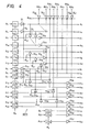
- Fig. 1 is a circuit block diagram of one embodiment in the case of applying the present invention to a 16-bit microprocessor.
- a portion enclosed with a chain line A is formed on a single semiconductor substrate such as single-crystal silicon by known semiconductor production technology.
- circuit symbol CPU shown by circuit symbol CPU is a microprocessor portion.
- this microprocessor portion CPU is constructed of, for example, an execution unit EXEC which is composed of an arithmetic-logic unit, dedicated registers such as a program counter, a stack pointer, a status register, and general-purpose registers for use as work areas, and a controller CONT which is composed of an instruction register to which microprogram instructions read out from an external memory not shown are successively input, micro ROMs in which microinstructions corresponding to respective macroinstructions are stored, and so on.
- EXEC which is composed of an arithmetic-logic unit, dedicated registers such as a program counter, a stack pointer, a status register, and general-purpose registers for use as work areas
- controller CONT which is composed of an instruction register to which microprogram instructions read out from an external memory not shown are successively input, micro ROMs in which microinstructions corresponding to respective macroinstructions are stored, and so on.
- the execution unit EXEC is operated in a proper sequence which is determined by control signals delivered from the controller CONT. Thus, desired data processing is executed. Coupled to the controller CONT are external terminals CT which are supplied with interrupt signals and reset signals.
- an oscillator OSC and a clock pulse generator CPG are provided.
- the oscillator OSC has its oscillation frequency determined by a circuit element, such as quartz vibrator or ceramics vibrator not shown, which is coupled between external terminals XT 1 and XT 2 .
- the clock pulse generator CPG receives the oscillation output of the oscillator OSC and properly divides its frequency, thereby to form a system clock P.
- a refresh counter RC which generates a refresh address of a dynamic RAM
- an address multiplexor MPX which selects either the address from the refresh counter RC or an address that is delivered from the execution unit EXEC to an address bus line A-BUS
- a control signal generator CSG which controls the operation of the address multiplexor MPX.
- the refresh counter RC is operated by the operating clock signal P of the system, and outputs a synchronizing signal RFSH indicative of the timing of refresh once in every about 2 milliseconds.
- the refresh counter RC also forms address signals for accessing the respective memory rows of the dynamic RAM, within the cycle of the synchronizing signal RFSH.
- the synchronizing signal RFSH is also fed to the microprocessor portion CPU and the control signal generator CSG.
- the microprocessor portion CPU When the synchronizing signal RFSH has been generated, the microprocessor portion CPU is prohibited from accessing the address bus A-BUS. Simultaneously therewith, switching control signals to be described in detail later are supplied from the control signal generator CSG to the address multiplexor MPX. In accordance with the switching control signals, the multiplexor MPX selects the refresh address supplied from the refresh counter RC, instead of the address signals on the address bus A-BUS. The address signals selected by the multiplexor MPX are output to an external address bus A-BUSE through an address buffer A-BFF.
- the synchronizing signal RFSH supplied from the refresh counter RC to the control signal generator CSG is externally fed as the signal RFSH indicative of the refresh timing.
- a plurality of address spaces to correspond to a plurality of sorts of memories and data indicating the attributes of the respective memories are set in the microprocessor in order to permit the memories to be simultaneously coupled to external address terminals AT.
- the embodiment is provided for discriminating the plurality of address spaces with two address setting registers AR 1 and AR 2 , two comparators COMP and COMP 2 which compare the contents of the address setting registers AR 1 and AR 2 with the address delivered from the microprocessor portion CP onto the address bus A-BUS and decide the relations of magnitudes thereof, respectively, and a decision circuit DCD which decides which address range the address signal on the address bus A-BUS falls within, by reference to the outputs of the two comparators COMP 1 and COMP 2 .
- Each of the address setting registers AR 1 and AR 2 has its operation controlled by the control signal delivered from the execution unit EXEC of the microprocessor portion CPU, and has address data written therein through a data bus D-BUS.
- the data to be written into the address setting registers AR 1 and AR 2 is stored along with programs to be executed by the shown microprocessor, in an unshown ROM the address terminals of which are coupled to the external address bus lines A-BUSE and the data output terminals of which are coupled to external data bus lines D-BUSE.
- the data is set in the address setting registers AR 1 and AR 2 as follows by way of example.
- the data to be written into the register AR 1 is read out from the unshown ROM and is once written into an unshown working register within the execution unit EXEC through a data buffer D-BFF as well as the internal data bus lines D-BUS. Subsequently, the data of the working register is output to the internal data bus D-BUS, and the control signal for writing the data into the register AR 1 is output from the execution unit EXEC. Thus, the data of the data bus line D-BUS is written into the register AR 1 . Also the register AR 2 has the data written thereinto according to a similar operating sequence.
- the whole memory space can be divided in three in accordance with the data set in the two address setting registers AR 1 and AR 2 .
- the address data of the address setting register AR 1 signifies the head address of the second address space among the first to third address spaces
- that of the address setting register AR 2 signifies the head address of the third address space.
- the data of the register AR makes it possible to identify the boundary between the first address space and the second address space, and that of the register AR 2 makes it possible to identify the boundary between the second address space and the third address space.
- the first address space is set to an address range from “000000” to "3FFFFF”
- the second address space is set to an address range from "400000” to "AFFFFF”.
- the third address space is set to a range from "BOOOOO" to "FFFFFF”.
- the ranges of the address data supplied from the CPU to the address bus lines A-BUS are decided by the comparators COMP 1 , COMP 2 and the decision circuit DCD.
- the comparator COMP 1 compares the address data of the address bus lines A-BUS with the data set in the register AR 1 . This comparator COMP 1 outputs "1" if the address data of the address bus lines A-BUS is greater than that of the register AR 1 , and it outputs "0" if not.
- the comparator COMP Z outputs "1" if the address data of the address bus lines A-BUS is greater than that of the register AR 2 , and it outputs "0" if not.
- the decision circuit DCD is, in effect, constructed of a decoder which decodes the outputs of the comparators COMP 1 and COMP 2 .
- the decision circuit DCD On the basis of the outputs of the comparators COMP 1 and COMP 2 , the decision circuit DCD provides three sorts of control signals which indicate the address spaces of the data of the address bus lines A-BUS.
- the output of the decision circuit DCD is used as the operation control signals of selecting circuits SEL 1 and SEL 2 to be described later.
- registers CR 1 - CR 3 each including stages B 0 - B 2 in which the data indicating the property of the memory corresponding to the address range is written.
- the configuration registers CR 1 to CR 3 have the setting of data therein controlled by the CPU. That is, the data for the configuration registers CR 1 to CR 3 is supplied through the data bus D-BUS.
- bit B O is used for data which corresponds to the addressing mode of the memory to be externally connected through the external bus lines A-BUSE and D-BUSE, and the bits B 1 and B 2 are used for data which corresponds to the storage capacity of the memory to be externally connected.
- the bit B 0 is set at "1" for a memory of the address multiplexing system such as a dynamic RAM, in other words, for a memory to which two kinds of address data items such as a row-group address and a column-group address are to be supplied in time division, and it is set at "0" for a memory to which two kinds of address data items are to be simultaneously supplied, such as a ROM or a static RAM.
- the two bits consisting of the bits B 1 and B 2 correspond to four sorts of storage capacities.
- the combinations of the bits B 1 and B 2 ; "00", “01”, “10” and “11” correspond respectively to the storage capacities of 16 kilobits, 64 kilobits, 256 kilobits and 1 megabit.
- the address setting registers AR 1 and AR 2 are respectively set at "400000” and "BOOOOO" in hexadecimal numbers and where the bits B 0 of the configuration registers CR 1 - CR 3 are respectively set at '0', '1' and '0'.
- the value '0' of the bit B 0 signifies the address range of the ROM or the static RAM other than the dynamic RAM
- the value '1' of the bit B 0 signifies the address range of the dynamic RAM, as described before.
- the address range of addresses "000000” to "3FFFFF” as illustrated in Fig. 2 becomes the first address space or address region ASP 1 directed to the static RAM or the ROM
- the address range of addresses "400000” to "AFFFFF” becomes the second address space ASP 2 directed to the dynamic RAM
- the address range of addresses "BOOOOO" to "FFFFFF” becomes the third address space ASP3 directed to the ROM or the static RAM.
- the information items of the bits B 0 of the respective configuration registers CR 1 - CR 3 are passed through the selecting circuit SELl whose switching operation is effected with the decision output signal of the decision circuit DCD, whereby one of the information items is selectively supplied to the control signal generator CSG. More specifically, if the address delivered onto the address bus A-BUS lies between "000000" and "3FFFFF", the selecting circuit SEL 1 which is controlled by the output of the decision circuit DCD at that time functions to supply the control signal generator CSG with the content of the bit B 0 of the configuration register CR 1 .
- the decision circuit DCD, the configuration registers CR 1 - CR 3 and the selecting circuit SELL constitute address decision means.
- the control signal generator CSG forms control signals with which address data items A 0 - A 23 on the address bus A-BUS are passed through the address multiplexor MPX as they are, so as to be supplied to the address buffer A-BFF, and it delivers the control signals to the address multiplexor MPX.
- the control signal generator CSG causes a latch circuit (not shown) within the address multiplexor MPX to accept the signal of a part corresponding to upper bits (or lower bits) required for accessing the dynamic RAM, among the address data items delivered from the microprocessor portion CPU onto the address bus A-BUS, and it allows the signal of a part corresponding to the lower bits (or the upper bits) of the address, to pass through the address multiplexor MPX as it is, thereby to deliver this signal as a row address signal.
- control signal generator CSG functions to send the upper bits (or lower bits) of the address already held in the latch circuit within the address multiplexor MPX, from the address multiplexor MPX to the address buffer A-BFF and to externally deliver them as a column address signal from the same address terminals as those of the row address signal.
- the upper bits and the lower bits of the address are delivered out individually, namely, by the address multiplexing system.
- a RAS signal row address strobe signal
- the control signal generator CSG in synchronism with this row address signal as shown in Fig. 3
- a CAS signal column address strobe signal
- the dynamic RAM connected to the microprocessor of this embodiment is accessed in synchronism with the falling edges of the RAS signal and the CAS signal and by accepting the addresses delivered from the address buffer A-BFF at those times, whereby desired data can be read out.
- the data bus D-BUS has the data buffer D-BFF connected thereto, the latter serving to input and output data between it and the unshown external memories through external data terminals DT as illustrated in Fig. 1.
- the information items of the sets of the bits B 1 and B 2 in the configuration registers CR 1 - CR 3 pass through the selecting circuit SEL 2 whose switching state is controlled by the output of the decision circuit DCD, whereby one of the sets is sent to the control signal generator CSG.
- the bits B 1 and B 2 of any of the configuration registers CR 1 - CR 3 subject to the bit B 0 being set at '1' are set at '0, 0' by way of example, they indicate that the capacity of the corresponding dynamic RAM is 16 kbits, as stated before.
- the control signal generator CSG When supplied with the information items of the bits B 1 and B 2 of any of the configuration registers CR 1 - CR 3 , the control signal generator CSG operates subject to these bits being '0, 0', to recognize 14 bits (for example, A 1 - A 14 ) in the signal on the address bus A-BUS as the formal address of the dynamic RAM and to latch half (A 8 - A 14 ) of the bits in the address multiplexor MPX and pass the remaining half (A 1 - A 7 ) therethrough without any change. Thereafter, the circuit CSG causes the address multiplexor MPX to deliver the half (A 8 - A 14 ) to the same external terminals.
- the control signal generator CSG operates to recognize 16 bits (for example, A 1 - A 16 ) in the signal on the address bus as the formal address and to latch half (A 9 - A 16 ) of the bits in the multiplexor MPX and pass the remaining half (A 1 - A 8 ) therethrough without any change.
- the control signal generator CSG similarly operates to halve the signal of 18 bits or 20 bits and deliver it in two divided steps.
- the bits not used for the access to the dynamic RAM are once latched in the address multiplexor MPX and are successively delivered out while the lower bits and upper bits are sequentially output as stated above.
- An address decoder installed on a memory board forms a chip select signal on the basis of the delivered bits so as to select the dynamic RAM.
- the signal which is supplied from the selecting circuit SELl to the control signal generator CSG and which indicates the information specifying whether or not the address range is of the dynamic RAM is delivered out as a signal DRAM. Owing to this signal DRAM, whether or not the microprocessor is accessing the dynamic RAM can be known. It is also possible, for example, to use this signal as the chip select signal of the dynamic RAM or to bring the ROM or the static RAM into an unselected state with this signal.
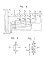
- Fig. 4 shows a practicable circuit arrangement of the multiplexor MPX.
- the multiplexor MPX is constructed of latch circuits LT 1 thru LT 24 the input terminals of which are coupled to corresponding address lines A 1 thru A 20 , A 0 , and A 21 thru A 23 constituting the address bus and the data accepting timings of which are controlled by a timing signal ⁇ l , and inverter circuits IV 1 thru IV 47 .
- inverter circuits IV 1 thru IV 47 those IV 1 thru IV 8 , IV 13 thru IV 27 , and IV 38 thru IV 47 are clocked inverter circuits the operations of which are respectively controlled by timing signals ⁇ r0 , ⁇ c0 thru ⁇ c6 , and ⁇ ref .
- each of the clocked inverter circuits is constructed, as shown in Fig. 7, of P-channel output MOSFETs Q 3 and Q 4 which are serially connected between a power source terminal V DD and an output terminal OUT, and N-channel MOSFET s Q 5 and Q 6 which are serially connected between the output terminal OUT and the ground point of the circuit.
- the MOSFETs Q 4 and Q S have their gates coupled to an input terminal IN, the MOSFET Q 6 has its gate coupled to a control line ⁇ , and the MOSFET Q 3 has its gate coupled to the control line ⁇ through an inverter IV60.
- the clocked inverter circuit of the above arrangement is responsively brought into an operating state and supplies the output terminal OUT with an output signal which is inverted in level with respect to an input signal fed to the input terminal IN.
- the control signal ⁇ is at a low level
- the clocked inverter circuit is brought into a latch state. That is, the output of the clocked inverter circuit is held at a previous output level irrespective of the level of an input signal by a holding capacitance not shown, e. g., a stray capacitance coupled to the output terminal.
- Fig. 6 shows a circuit example of the inverter circuit.
- the clocked inverter circuits IV 5 thru IV 8 , IV 14 , IV 16 , IV 18 , and I V 22 thru IV 27 can be regarded as column selection circuits as will be understood from later description.
- the clocked inverter circuits IV 38 thru IV 47 in Fig. 4 have their respective input terminals RA 0 thru RA9 coupled to the output terminals of the refresh counter RC in Fig. 1.
- the timing signals or control signals ⁇ l , ⁇ r0 , ⁇ c0 thru ⁇ c6 , and ⁇ ref for controlling the operation of the multiplexor MPX are produced from the control signal generator CSG.
- Fig. 5 is a circuit diagram of part of the control signal generator CSG.
- the control signal ⁇ ref which is supplied to the circuit in Fig. 5 is formed, for example, in such a way that the refresh control signal RFSH delivered from the refresh counter RC in Fig. 1 is inverted by an inverter circuit.
- the timing signal ⁇ r0 is, in effect, regarded as an upper- (or lower-) bit select signal.
- This timing signal ⁇ r0 is brought to the high level or "1" level in the first half of the cycle of the clock signal ⁇ (hereinbelow, termed the first cycle) if the bit signal B 0 delivered from the selecting circuit SELl in Fig. 1 is "1", in other words, if the bit B 0 of the configuration register selected by the selecting circuit SEL 1 indicates the address multiplexing system, and it is brought to the high level in the first cycle and the succeeding second cycle if the bit signal B O is "0".
- the timing signal ⁇ r0 is responsively brought to the low level or "0" level if the refresh control signal RFSH is at the low level, that is, it indicates the refresh operation.
- timing signal ⁇ r0 is as follows by way of example.
- the circuit is constructed of a pulse formation circuit which receives the output of the clock pulse generator CPG in Fig. 1, thereby to form a first clock signal having the aforementioned first cycle and a second clock signal having the aforementioned first and second cycles; a first gate circuit made up of an AND circuit which forms the logical product signal among the bit signal B 0 delivered from the selection circuit SEL 1 , the first clock signal, and the control signal RFSH; a second gate circuit made up of an AND circuit which forms the logical product signal among the inverted signal of the bit signal B 0' the second clock signal, and the control signal RFSH; and a third gate circuit which forms the logical sum signal between the outputs of the first and second gate circuits.
- an AND circuit is composed of a NAND circuit and an inverter circuit
- an OR circuit is composed of a NOR circuit and an inverter circuit.
- the timing signal ⁇ c0 is regarded as a lower (or upper) bit select signal.
- This timing signal ⁇ c0 is held at the high level in the aforementioned second cycle if the bit signal B 0 output from the selection circuit SEL 1 in Fig. 1 is "1", whereas it is held at the "0" level or low level in response to the value "0" of the bit signal B 0 , as well as the low level ("0" level) of the signal RFSH.
- the timing signal ⁇ c0 is generated by an AND circuit which forms the logical product signal among the first and second clock signals, the inverted signal of the bit signal B 0 , and the control signal RFSH.
- a gate circuit G 11 made up of an AND circuit has its output brought to the "1" level or high level responsively when the bit signals Bland B 2 supplied from the selection circuit SEL 2 in Fig. 1 are "0" and "0", in other words, when the combination of the bit signals Bland B 2 indicates a memory requiring address signals of 14 bits, such as a 16-kilobit memory of 1-bit format.
- a gate circuit G 12 has its output brought to the "1" level responsively when the bit signals Bland B 2 are "1" and "0” respectively, in other words, when they indicate a memory requiring address signals of 16 bits, such as a 64-kilobit memory of 1-bit format.
- the outputs of gate circuits G 13 and G 14 are brought to the "1" level when the bit signals B 1 and B 2 indicate a memory requiring address signals of 18 bits, such as a 256-kilobit memory of 1-bit format, and a memory such as a 1-megabit memory, respectively.
- a gate circuit G 1 made up of an AND circuit receives the output of the gate circuit G 11 and the timing signal ⁇ c0 . Therefore, when the bit signals B 1 and B 2 indicate the 16-kilobit memory, the output ⁇ c1 of this gate circuit G 1 is brought to the "1" level in synchronism with the timing signal ⁇ c0 .
- a gate circuit G 2 receives the output of an OR gate circuit G 7 supplied with the output of the gate circuit G 11 or G 12 , together with the timing signal ⁇ c0' Therefore, when the bit signals B 1 and B 2 indicate the 16-kilobit or 64-kilobit memory, the output ⁇ c2 of this gate circuit G 2 is brought to the "1" level in synchronism with the timing signal ⁇ c0 .
- the timing signal ⁇ c3 which is output from a gate circuit G 3 is brought to the "1" level in synchronism with the timing signal ⁇ c0 when the combination of the bit signals B 1 and B 2 indicates the 16-kilobit, 64-kilobit or 256-kilobit memory
- the timing signal ⁇ c4 which is output from a gate circuit G 4 is brought to the "1" level in synchronism with the timing signal ⁇ c0 when the bit signals B 1 and B 2 indicate the 64-kilobit, 256-kilobit or 1-megabit memory.
- the timing signal ⁇ c5 ' is brought to the "1" level in synchronism with the timing signal ⁇ c0' and if the bit signals B 1 and B 2 indicate the.1- megabit memory, the timing signal ⁇ c6 is brought to the "1" level in synchronism with the timing signal ⁇ c0 .
- the address multiplexor MPX in Fig. 4 is operated in response to the timing signals which are output from the control signal generator CSG in Fig. 5.
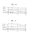
- Fig. 8 shows a timing chart in the case where the 16-kilobit DRAM is accessed.
- the outputs a 1 thru a 7 of the multiplexor MPX are supplied to the address terminals of such a DRAM through the address buffer A-BFF and the external bus lines A-BUSE in Fig. 1.
- the circuit operations will be described by utilizing the timing chart of Fig. 8.
- the timing signal ⁇ l for the latch circuits LT 1 thru LT 24 is brought to the high level in synchronism with the timing at which the address signals are supplied to the address bus lines A-BUS.
- the latch circuits LT 1 thru LT 24 accept the address signals of the address bus lines A-BUS in response to the timing signal ⁇ l .
- the timing signal ⁇ r0 is held at the high level for a period from a time to to a time t 1 in accordance with the fact that the bit signal B 0 supplied to the control signal generator CSG in Fig. 1 is "I".
- the clocked inverter circuits IV 1 thru IV 4 and I V 19 thru IV 21 in Fig. 4 are brought into their operating states in response to the timing signal ⁇ r0 rendered the high level.
- the outputs a 1 thru a4 and a 5 thru a 7 of the multiplexor MPX are respectively brought to levels corresponding to the address signals A 1 thru A 7 of the address bus lines A-BUS.
- the timing signal ⁇ c0 is brought to the high level in synchronism with the timing at which the timing signal ⁇ r0 is rendered the low level.
- the timing signals ⁇ c1 thru ⁇ c3 are brought to the high level in synchronism with the timing signal ⁇ c0 as illustrated at D in Fig. 8 because the bit signals B 1 and B 2 supplied to the control signal generator CSG in Fig. 1 are "0" and "0" indicative of the 16-kilobit memory.
- the remaining timing signals ⁇ c4 thru ⁇ c6 are held at the low level irrespective of the timing signal ⁇ c0 as illustrated at E in Fig. 8.
- the clocked inverter circuits IV 5 thru IV 8 in Fig. 4 are brought into their operating states in response to the timing signal ⁇ c0 rendered the high level, and those IV 14 , IV 16 and I V 18 are brought into their operating states in response to the respective timing signals ⁇ c1' ⁇ c2 and ⁇ c3 rendered the high level.
- the respective levels of the outputs a 1 thru a 4 of the multiplexor MPX are determined by the inverter circuits IV 5 thru IV 8 .
- the respective levels of the outputs a 5 thru a 7 are determined by the inverter circuits IV 14 , IV 16 and IV 18 .
- the inputs of the inverter circuits IV 5 thru IV 8' the input of the inverter circuit IV 14 , and the inputs of the inverter circuits IV 16 and IV 18 are respectively coupled to the latch circuits LT 5 thru LT 8' LT 9 , and LT 10 and LT 11 .
- the outputs a 1 thru a4 and a 5 thru a 7 of the multiplexor MPX are therefore brought to levels corresponding to the address signals All thru A 14 , A 8 , A 9 and A 10 respectively as illustrated at F in Fig. 8, in response to the timing signals ⁇ c0 thru ⁇ c3 rendered the high level.
- the timing signal ⁇ r0 for the clocked inverter circuits IV 1 thru IV 4 and IV 19 thru IV 21 is brought to the low level in synchronism with the timing at which the clocked inverter circuits IV 5 thru IV 8 , IV 14 , IV 16 and IV 18 are operated. Therefore, the inverter circuits IV 1 thru I V 4 and IV 19 thru I V 21 do not affect the output levels of the inverter circuits IV 5 thru IV B , IV 14 , IV 16 and IV 18 .
- the outputs a 1 thru a 7 determined at the time t 0 are set as the row address signals for the 16-kilobit DRAM, and the outputs a 1 thru a 7 determined at the time t 1 are set as the column address signals.
- the outputs a 1 thru a 7 are maintained at the previous levels by means of holding capacitances such as stray capacitances existent in the respective output lines even when the timing signals ⁇ c0 thru ⁇ c3 are returned from the high level to the low level thereby to bring the clocked inverter circuits IV 5 etc. into their non-operating states. These outputs a 1 thru a 7 are updated in response to the timing signal ⁇ r0 rendered the high level again.
- the outputs a 0 and a 15 thru a 23 which need not be address-multiplexed have their respective levels determined at the time t 0 as illustrated at G in Fig. 8. That is, the outputs a 0 and a 15 thru a 23 have their respective levels determined by the static inverter circuits IV34, IV 28 thru IV 33 and IV 35 thru IV37 which receive the outputs of the latch circuits LT 21 , LT 15 thru LT20 and LT 22 thru LT 24 .
- the outputs a 8 thru a 14 are brought to levels corresponding respectively to the address signals A 8 thru A 14 at the time t 0 . Since these outputs as thru a 14 are not supplied to the address input terminals of the 16-kilobit DRAM, they may well be maintained at the levels corresponding to the address signals A 8 thru A 16 .
- the address signals A 8 thru A 14 are supplied to the outputs a 1 thru a 7 after altering the order thereof properly.
- the address signal A 8 is not supplied to the output a l but is supplied to the output a 5 .
- the address signal A 9 is not supplied to the output a 2 (not shown) but is supplied to the output a 9 .
- Such alterations merely signify that the correspondence between logic addresses indicated by the address signals A 1 thru A 14 and the physical addresses of the DRAM is changed.
- Fig. 9 shows a timing chart in the case where the 64-kilobit DRAM is accessed.
- the timing signals ⁇ c1 , ⁇ c5 and ⁇ c6 are held at the low level as shown at E and H in Fig. 9, in response to the respective values "1" and "0" of the bit signals B 1 and B 2 (C and D in Fig. 9) and irrespective of the timing signal ⁇ c0 (B in Fig. 9).
- the timing signals ⁇ c2' ⁇ c3 and ⁇ c4 are brought to the high level in synchronism with the the timing signal ⁇ c0 .
- the outputs a 1 thru a 8 of the multiplexor MPX are brought to levels corresponding to the respective address signals A 1 thru A 8 in response to the timing signal ⁇ r0 rendered the high level at a time t 0 , and they are brought to levels corresponding to the respective address signals A 9 thru A 16 in response to the timing signals ⁇ c0 and ⁇ c2 thru ⁇ c4 rendered the high level at a time t l .
- the outputs a 0 and a 17 thru a 23 are brought to levels corresponding respectively to the address signals A O and A 17 thru A 23 .
- Fig. 10 shows a timing chart of the refresh operation.
- timing signals ⁇ r0 and ⁇ c0 are held at the low level as illustrated at A and B in Fig. 10.
- the clocked inverter circuits IV 1 thru IV 8 and IV 13 thru IV 27 which are coupled to the latch circuits in Fig. 4 are brought into the non-operating states.
- the clocked inverter circuits IV 38 thru IV4 7 in Fig. 4 are responsively brought into the operating states.
- the outputs a 1 thru a 10 of the multiplexor MPX are brought to levels corresponding to the respective address signals RA 0 thru RA 9 delivered from the refresh counter RC in Fig. 1, as illustrated at D in Fig. 10.
- the DRAM not shown, which is coupled to the external bus lines A-BUSE in Fig.
- Fig. 11 shows a timing chart in the case where the SRAM or ROM which is not of the address multiplexing system is accessed.
- timing signals ⁇ c0 and ⁇ c1 thru ⁇ c6 are all maintained at the low level as illustrated at B and C in Fig. 11.
- the outputs a 0 thru a 23 of the multiplexor MPX are brought to levels corresponding to the respective address signals A 0 thru A 23 in response to the timing signal ⁇ r0 (A in Fig. 11) rendered the high level at a time t 0 .
- the SRAM or ROM is accessed.
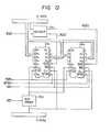
- Fig. 12 is a connection diagram of external memories.
- each of the external memories DM 1 and DM 2 is constructed of a dynamic RAM of 64 kbits which has address terminals A 0 - A 7 , a data output terminal DOUT, a column address strobe terminal CAS, a reference potential terminal (ground terminal) V ss , a refresh control terminal RFSH, a data input terminal DIN, a write enable terminal WE, a row address strobe terminal RAS and a power source terminal V cc .
- Each of the memories DM 1 and DM 2 is adapted to input/output data of one bit at a time.
- a plurality of memories are required for such data.
- an external address bus A-BUSE is coupled to the external address terminals AT in Fig. 1, and an external data bus D-BUSE is coupled to the external data terminals DT in Fig. 1.
- a decoder DEC forms row address strobe signals RAS 1 and RAS 2 to be supplied to the respective memories DM 1 and DM 2 , on the basis of an address signal of 1 bit supplied through the external address bus A-BUSE and a row address strobe signal supplied through the terminal RAS in Fig. 1.
- the address terminals A 0 - A 7 of the memories DM and DM 2 are fed with common address signals through the external address bus A-BUSE.
- the memory DM 1 is selected by the signal RAS 1 and the address signals applied to the address terminals A 0 - A 7
- the memory DM 2 is similarly selected by the signal RAS 2 and the signals of the address terminals A 0 - A 7 .
- the column address strobe terminals CAS, refresh control terminals RFSH and write enable terminals WE of the memories DM 1 and DM 2 are respectively connected in common to terminals CAS, RFSH and WR in Fig. 1.
- the data output terminals DOUT of the memories DM 1 and DM 2 are connected in common to the input terminal of a bus driver TSC, and the data input terminals DIN are connected to the external data bus D-BUSE, along with the output terminal of the bus driver TSC.
- the bus driver TSC is constructed of a tri-state circuit which, subject to the low level of a read control signal RD supplied thereto, produces at its output terminal an output signal of a level corresponding to an input signal supplied to its input terminal. If the signal RD is at its high level, the output of the bus driver TSC is brought into a high impedance state.
- the refresh counter RC is built in the microprocessor as shown in Fig. 1, and when the refresh address of this refresh counter RC is to be provided externally, the signal RFSH indicative of the corresponding timing is output. Therefore, a complicated refresh control circuit for forming the refresh signal of the dynamic RAM need not be constructed by an external circuit.
- the microprocessor of this embodiment includes therein the register for setting the address range of the dynamic RAM, and when any address of the dynamic RAM is to be accessed, the address is automatically multiplexed within the chip.
- the dunamic RAM can be accessed as simply as the static RAM without disposing any external circuit.
- the read and write controls of the dynamic RAM are executed in accordance with the read control signal RD and write control signal WR which are output from the microprocessor portion CPU.
- the address range of the dynamic RAM can be set at will by setting proper addresses in the address setting registers AR 1 and AR 2 .
- the above embodiment is generally used in such a way that the bits B 0 of the configuration registers CR I - CR 3 are reset to "0" in a reset state, thereby to first establish a ROM access state and execute a program in the ROM, whereupon the address setting registers AR 1 and AR 2 are previously set in conformity with the system arrangement. It is also possible, however, to alter the set values of the address setting registers AR 1 and AR 2 in the course of the program so as to change the address range of the dynamic RAM.
- the respective address spaces which are set by the address setting registers AR 1 and AR 2 may correspond to a plurality of sorts of memories.
- the ROM and the static RAM which have the same addressing system can correspond within a single address space. In this case, a partial address space in the single address space is caused to correspond to the ROM, and another partial address space is caused to correspond to the static RAM.
- the configuration registers CR 1 - CR 3 are furnished with the bits B 1 and B 2 indicating the capacities of the dynamic RAMs, so that a system can be constructed using the RAMs which have any desired capacities of 16 kbits - 1 Mbits.
- those bits of each of the configuration registers CR 1 - CR 3 which indicate the capacity of the dynamic RAM are not restricted to the 2 bits B 1 and B 2 as in the embodiment, but they may well be replaced with 1 bit or with 3 or more bits.
- 2 bits may well be used instead of the 1 bit B O indicating the information as to whether or not the address range of the dynamic RAM is concerned, thereby making it possible to distinguish the address ranges of the ROM and the static RAM.
- the configuration registers CR 1 - CR 3 may well be furnished with bits which bear information other than the foregoing (for example, a bit which indicates whether a corresponding address area is read-only or read/write, a bit which indicates whether a program or data is concerned, and a bit which indicates whether a system area or a user area is concerned).
- the two address setting registers are disposed so as to make it possible to trisect the address space owned by the microprocessor.
- the number of the registers is not restricted to 2, but 1 register or at least 3 registers can also be disposed.
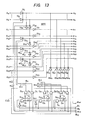
- Fig. 13 is a circuit diagram of an address multiplexor MPX and a part of a control signal generator CSG in another embodiment.
- timing signals ⁇ r0 , ⁇ c0 and ⁇ ref in the control signal generator CSG are respectively the same as those of the preceding embodiment.
- an inverter circuit IV 45 and an AND gate circuit G 1 constitute a decoder which forms an output signal of high level when bit signals Bland B 2 are "1" and "0" respectively, namely, when the bit signals B 1 and B 2 indicates a memory such as 64-kilobit memory of 1-bit format.
- a timing signal ⁇ r1 to be output from an OR gate circuit G 2 is brought to the high level in synchronism with the timing signal ⁇ r0 if the bit signals B 1 and B 2 indicate the 64-kilobit memory, and it is maintained at the high level irrespective of the timing signal ⁇ r0 unless the bit signals B l and B 2 indicate the 64-kilobit memory.
- a timing signal ⁇ r2 to be output from an OR gate circuit G 6 is brought to the high level in synchronism with the timing signal ⁇ r0 if the bit signals B 1 and B 2 are "0" and "1" respectively, namely, if they indicate a memory such as 256-kilobit memory of 1-bit format, and it is maintained at the high level irrespective of the timing signal ⁇ r0 if they are not.
- a timing signal ⁇ r3 to be output from an OR gate circuit G 10 is brought to the high level in synchronism with the timing signal ⁇ r0 if the bit signals B 1 and B 2 are "1" and "1", namely, if they indicate a memory such as 1-megabit memory of 1-bit format, and it is maintained at the high level if they are not.
- a timing signal ⁇ c1 to be output from an AND gate circuit G 4 is brought to the high level, only when the bit signals B I and B 2 indicate the 64-kilobit memory and besides the timing signal ⁇ c0 is brought to the high level.
- a timing signal ⁇ c2 to be output from an AND gate circuit G 8 is brought to the high level, only when the bit signals B 1 and B 2 indicate the 256- kilobit memory and besides the timing signal ⁇ c0 is brought to the high level.
- a timing signal ⁇ c3 is brought to the high level, only when the bit signals B 1 and B 2 indicate the 1-megabit memory and besides the timing signal ⁇ c0 is brought to the high level.
- the multiplexor MPX is constructed of clocked inverter circuits IV 0 thru IV 6 , I V 24 thru IV 30 , IV 14 , IV 31 , IV 16 , IV 32 , IV 18 , and I V 33 and static inverter circuits IV 7 thru IV 13 , IV 15 , IV 17 , and IV 19 thru IV 23' the input terminals of which receive the address signals A 0 thru A 23 at the address bus lines A-BUS in Fig. 1, and clocked inverter circuits IV 34 thru IV4 3 , the input terminals of which receive the respective outputs RA 0 thru RA 9 of the refresh counter RC in Fig. 1.
- the address signals A 0 thru A 6 are regarded as the row address signals, and those A 7 thru A 13 are regarded as the column address signals.
- the outputs a 0 thru a 6 of the multiplexor MPX are supplied to the address terminals of the DRAM.
- the outputs a O thru a 6 are rendered levels corresponding to the address signals A 0 thru A 6 when the timing signal ⁇ r0 is rendered the high level, because the inverter circuits IV 0 thru IV 6 are brought into their operating states in response to this high level, and they are rendered levels corresponding to the address signals A 7 thru A 13 when the timing signal ⁇ c0 is rendered the high level, because the inverter circuits IV 24 thru IV 30 are brought into their operating states in response to this high level.
- the outputs a 7 thru a 23 of the multiplexor MPX are held at levels corresponding to the respective address signals A 7 thru A 23 .
- the outputs a 7 thru a 13 have their respective levels determined by the static inverter circuits IV 7 thru IV 13 .
- the inverter circuits IV 14 , IV 16 etc. are put in their operating states because the timing signals ⁇ r1 , ⁇ r2 etc. are maintained at the high level without regard to the timing signal ⁇ r0 . Therefore, the outputs a 14 , a 16 etc. are brought to levels corresponding to the address signals A 14 , A 16 etc.
- the address signals A 0 thru A 6 and A 14 are regarded as the row address signals, and those A 7 thru A 13 and A 15 are regarded as the column address signals.
- the address signals A 7 thru A 13 and A 15 are supplied to the outputs a 0 thru a 6 and a 14 at the timing of the timing signal ⁇ c0 . Therefore, the outputs a 0 thru a 6 and a 14 are fed to the address input terminals of the DRAM through the address buffer A-BFF in Fig. 1.
- the address signals A 0 thru A 6 , A 14 and A 16 are regarded as the row address signals, and the address signals A 7 thru A 13 , A 15 and A 17 are regarded as the column address signals.
- the address signals A 0 thru A 6 , A 15 and A 17 are supplied to the outputs a 0 thru a 6 , a 14 and a 16 at the timing of the timing signal ⁇ c0 . Therefore, the outputs a 0 thru a 6 , a 14 and a 16 are supplied to the address input terminals of the DRAM.
- the address signals A 0 thru A 6 , A 14' A 16 and A 18 are regarded as the row address signals, and those A 7 thru A 13 , A 15 , A 17 and A 19 are regarded as the column address signals.
- the address signals A 7 thru A 13 , A 15' A 17 and A 19 are supplied to the outputs a 0 thru a 6 , a 14 , a 16 and a 18 at the timing of the timing signal ⁇ c0 . Therefore, the outputs a 0 thru a 6 , a 14' a 16 and a 18 are supplied to the address input/output terminals of the DRAM.
- the timing signals ⁇ r0 and ⁇ c0 are brought to the low level and the refresh control signal ⁇ ref is brought to the high level as in the preceding embodiment.
- the clocked inverter circuits IV 34 thru I V 43 in Fig. 13 are brought into their operating states, and the outputs RA 0 thru RA 9 of the refresh counter RC in Fig. 1 are supplied to the outputs a 0 thru a 6 , a 14 , a 16 and a 16 through these inverter circuits IV 34 thru I V 4 3.
- the timing signal ⁇ c0 in the circuit of Fig. 13 is maintained at the low level as in the preceding embodiment.
- the timing signals ⁇ c1 thru ⁇ c3 are maintained at the low level in accordance with the timing signal ⁇ c0 .
- the column selection circuits namely, the clocked inverter circuits IV 24 thru IV 30 and I V 31 thru IV 33 are put in their non-operating states.
- the outputs a 0 thru a 23 are brought to levels corresponding to the address signals A 0 thru A 23 in synchronism with the timing signal ⁇ r0 .
- the address range of a dynamic RAM is made variable by a register, but it is also possible to replace the register with means to generate a fixed address and to fixedly divide an address space.
- configuration registers CR l - CR 3 themselves may well be omitted so as to uniquely designate which memory an address range divided by the address setting registers AR 1 and AR 2 belongs to, in accordance with the decision output of the decision circuit DCD and to operate the address multiplexor MPX in correspondence therewith.
Landscapes
- Engineering & Computer Science (AREA)
- Theoretical Computer Science (AREA)
- Physics & Mathematics (AREA)
- General Engineering & Computer Science (AREA)
- General Physics & Mathematics (AREA)
- Dram (AREA)
- Microcomputers (AREA)
- Memory System (AREA)
- Document Processing Apparatus (AREA)
- Digital Computer Display Output (AREA)
Applications Claiming Priority (2)
| Application Number | Priority Date | Filing Date | Title |
|---|---|---|---|
| JP248109/84 | 1984-11-26 | ||
| JP59248109A JPH0642263B2 (ja) | 1984-11-26 | 1984-11-26 | デ−タ処理装置 |
Publications (3)
| Publication Number | Publication Date |
|---|---|
| EP0183231A2 true EP0183231A2 (de) | 1986-06-04 |
| EP0183231A3 EP0183231A3 (en) | 1989-02-15 |
| EP0183231B1 EP0183231B1 (de) | 1993-02-24 |
Family
ID=17173359
Family Applications (1)
| Application Number | Title | Priority Date | Filing Date |
|---|---|---|---|
| EP85115002A Expired - Lifetime EP0183231B1 (de) | 1984-11-26 | 1985-11-26 | Datenprozessor |
Country Status (7)
| Country | Link |
|---|---|
| US (3) | US4792891A (de) |
| EP (1) | EP0183231B1 (de) |
| JP (1) | JPH0642263B2 (de) |
| KR (3) | KR930002323B1 (de) |
| DE (1) | DE3587116T2 (de) |
| HK (1) | HK28696A (de) |
| SG (1) | SG59880G (de) |
Cited By (3)
| Publication number | Priority date | Publication date | Assignee | Title |
|---|---|---|---|---|
| EP0473274A3 (en) * | 1990-08-31 | 1992-04-01 | Advanced Micro Devices, Inc. | Memory bank comparator system |
| US5241665A (en) * | 1990-08-31 | 1993-08-31 | Advanced Micro Devices, Inc. | Memory bank comparator system |
| WO1997027547A3 (en) * | 1996-01-27 | 1997-10-16 | Motorola Israel Ltd | Dynamic ram in a microprocessor system |
Families Citing this family (35)
| Publication number | Priority date | Publication date | Assignee | Title |
|---|---|---|---|---|
| US5187799A (en) * | 1988-05-17 | 1993-02-16 | Calif. Institute Of Technology | Arithmetic-stack processor which precalculates external stack address before needed by CPU for building high level language executing computers |
| US5283885A (en) * | 1988-09-09 | 1994-02-01 | Werner Hollerbauer | Storage module including a refresh device for storing start and stop refresh addresses |
| US5193193A (en) * | 1988-09-14 | 1993-03-09 | Silicon Graphics, Inc. | Bus control system for arbitrating requests with predetermined on/off time limitations |
| US5179667A (en) * | 1988-09-14 | 1993-01-12 | Silicon Graphics, Inc. | Synchronized DRAM control apparatus using two different clock rates |
| JPH02260195A (ja) * | 1989-03-30 | 1990-10-22 | Mitsubishi Electric Corp | リフレッシュコントロール回路 |
| US5128563A (en) * | 1990-11-28 | 1992-07-07 | Micron Technology, Inc. | CMOS bootstrapped output driver method and circuit |
| US5206935A (en) * | 1991-03-26 | 1993-04-27 | Sinks Rod G | Apparatus and method for fast i/o data transfer in an intelligent cell |
| US5229969A (en) * | 1991-04-15 | 1993-07-20 | Micron Technology, Inc. | Method for synchronizing refresh cycles in self-refreshing DRAMs having timing circuit shutdown |
| US5229970A (en) * | 1991-04-15 | 1993-07-20 | Micron Technology, Inc. | Circuit for synchronizing refresh cycles in self-refreshing drams having timing circuit shutdown |
| US5208779A (en) * | 1991-04-15 | 1993-05-04 | Micron Technology, Inc. | Circuit for providing synchronous refresh cycles in self-refreshing interruptable DRAMs |
| JPH05113870A (ja) * | 1991-10-23 | 1993-05-07 | Mitsubishi Electric Corp | ソート処理プロセツサ |
| US6223264B1 (en) | 1991-10-24 | 2001-04-24 | Texas Instruments Incorporated | Synchronous dynamic random access memory and data processing system using an address select signal |
| JP3134450B2 (ja) * | 1992-02-17 | 2001-02-13 | 日本電気株式会社 | マイクロプロセッサ |
| US5402384A (en) * | 1992-04-24 | 1995-03-28 | Citizen Watch Co., Ltd. | Dynamic ram |
| US5363337A (en) * | 1992-07-15 | 1994-11-08 | Micron Technology, Inc. | Integrated circuit memory with variable addressing of memory cells |
| US5379400A (en) * | 1992-08-07 | 1995-01-03 | International Business Machines Corp. | Method and system for determining memory refresh rate |
| US5278801A (en) * | 1992-08-31 | 1994-01-11 | Hewlett-Packard Company | Flexible addressing for drams |
| JPH06150023A (ja) | 1992-11-06 | 1994-05-31 | Hitachi Ltd | マイクロコンピュータ及びマイクロコンピュータシステム |
| JP3244340B2 (ja) * | 1993-05-24 | 2002-01-07 | 三菱電機株式会社 | 同期型半導体記憶装置 |
| JPH0778106A (ja) | 1993-09-08 | 1995-03-20 | Hitachi Ltd | データ処理システム |
| JP3904244B2 (ja) * | 1993-09-17 | 2007-04-11 | 株式会社ルネサステクノロジ | シングル・チップ・データ処理装置 |
| KR950014089B1 (ko) * | 1993-11-08 | 1995-11-21 | 현대전자산업주식회사 | 동기식 디램의 히든 셀프 리프레쉬 방법 및 장치 |
| JPH07153266A (ja) * | 1993-11-26 | 1995-06-16 | Mitsubishi Electric Corp | Dram制御回路 |
| JP3563768B2 (ja) * | 1994-05-31 | 2004-09-08 | 株式会社ルネサステクノロジ | Romプログラム変更装置 |
| US5557578A (en) * | 1995-05-01 | 1996-09-17 | Apple Computer, Inc. | Dynamic memory refresh controller and method |
| US5557577A (en) * | 1995-05-01 | 1996-09-17 | Apple Computer, Inc. | System and method for performing wake-up operations to a memory |
| US5946703A (en) * | 1997-02-07 | 1999-08-31 | Silicon Integrated Systems Corp. | Method for reading data in data reading and writing system |
| US6327640B1 (en) * | 1997-03-07 | 2001-12-04 | Advanced Micro Devices, Inc. | Overlapping peripheral chip select space with DRAM on a microcontroller with an integrated DRAM controller |
| JP4722305B2 (ja) | 2001-02-27 | 2011-07-13 | 富士通セミコンダクター株式会社 | メモリシステム |
| WO2003067445A1 (en) * | 2002-02-06 | 2003-08-14 | Koninklijke Philips Electronics N.V. | Address space, bus system, memory controller and device system |
| US7117398B2 (en) * | 2002-11-22 | 2006-10-03 | Texas Instruments Incorporated | Program counter range comparator with equality, greater than, less than and non-equal detection modes |
| KR100653686B1 (ko) * | 2003-12-31 | 2006-12-04 | 삼성전자주식회사 | 동적 반도체 메모리 장치 및 이 장치의 절전 모드 동작방법 |
| US8267780B2 (en) | 2004-03-31 | 2012-09-18 | Nintendo Co., Ltd. | Game console and memory card |
| US7512029B2 (en) * | 2006-06-09 | 2009-03-31 | Micron Technology, Inc. | Method and apparatus for managing behavior of memory devices |
| KR100881196B1 (ko) * | 2007-05-29 | 2009-02-05 | 삼성전자주식회사 | 선택 가능한 두개의 비트 구조를 갖는 메모리 장치 및 이를구비하는 시스템 |
Family Cites Families (16)
| Publication number | Priority date | Publication date | Assignee | Title |
|---|---|---|---|---|
| DE2212922B2 (de) * | 1972-03-17 | 1976-02-05 | Karl Schmidt Gmbh, 7107 Neckarsulm | Gebauter kolben fuer verbrennungskraftmaschinen |
| US4332008A (en) * | 1976-03-09 | 1982-05-25 | Zilog, Inc. | Microprocessor apparatus and method |
| JPS53136924A (en) * | 1977-05-06 | 1978-11-29 | Fujitsu Ltd | Control system for memory device |
| DE2842548A1 (de) * | 1978-09-29 | 1980-04-10 | Siemens Ag | Programmierbare speicherschutzlogik fuer mikroprozessorsysteme |
| JPS5798600U (de) * | 1980-12-09 | 1982-06-17 | ||
| JPS57143652A (en) * | 1981-03-02 | 1982-09-04 | Fuji Electric Co Ltd | Extension system for memory unit |
| JPS57143651A (en) * | 1981-03-02 | 1982-09-04 | Nec Corp | Control system using in common the same test panel |
| JPS57203276A (en) * | 1981-06-09 | 1982-12-13 | Nippon Telegr & Teleph Corp <Ntt> | Information storage device |
| US4433378A (en) * | 1981-09-28 | 1984-02-21 | Western Digital | Chip topography for MOS packet network interface circuit |
| IT1142074B (it) * | 1981-11-24 | 1986-10-08 | Honeywell Inf Systems | Sistema di elaborazione dati con allocazione automatica dell'indirizzo in una memoria modulare |
| JPS58192148A (ja) * | 1982-05-07 | 1983-11-09 | Hitachi Ltd | 演算処理装置 |
| JPS59162691A (ja) * | 1983-03-07 | 1984-09-13 | Hitachi Ltd | ダイナミツクram |
| US4613953A (en) * | 1983-04-22 | 1986-09-23 | Ncr Corporation | Paging register for memory devices |
| US4755964A (en) * | 1985-04-19 | 1988-07-05 | American Telephone And Telegraph Company | Memory control circuit permitting microcomputer system to utilize static and dynamic rams |
| US4835733A (en) * | 1985-09-30 | 1989-05-30 | Sgs-Thomson Microelectronics, Inc. | Programmable access memory |
| JPH0458675A (ja) * | 1990-06-28 | 1992-02-25 | Toshiba Corp | 2値イメージ伸張方式 |
-
1984
- 1984-11-26 JP JP59248109A patent/JPH0642263B2/ja not_active Expired - Lifetime
-
1985
- 1985-11-20 US US06/799,795 patent/US4792891A/en not_active Expired - Lifetime
- 1985-11-21 KR KR1019850008718A patent/KR930002323B1/ko not_active Expired - Fee Related
- 1985-11-26 SG SG1995905782A patent/SG59880G/en unknown
- 1985-11-26 EP EP85115002A patent/EP0183231B1/de not_active Expired - Lifetime
- 1985-11-26 DE DE8585115002T patent/DE3587116T2/de not_active Expired - Lifetime
-
1990
- 1990-07-25 US US07/560,230 patent/US5021951A/en not_active Ceased
-
1993
- 1993-11-26 KR KR1019930025387A patent/KR940002086B1/ko not_active Expired - Fee Related
- 1993-11-26 KR KR1019930025388A patent/KR940002076B1/ko not_active Expired - Fee Related
-
1996
- 1996-02-15 HK HK28696A patent/HK28696A/en not_active IP Right Cessation
- 1996-10-11 US US08/729,132 patent/USRE36482E/en not_active Expired - Lifetime
Cited By (5)
| Publication number | Priority date | Publication date | Assignee | Title |
|---|---|---|---|---|
| EP0473274A3 (en) * | 1990-08-31 | 1992-04-01 | Advanced Micro Devices, Inc. | Memory bank comparator system |
| US5241665A (en) * | 1990-08-31 | 1993-08-31 | Advanced Micro Devices, Inc. | Memory bank comparator system |
| WO1997027547A3 (en) * | 1996-01-27 | 1997-10-16 | Motorola Israel Ltd | Dynamic ram in a microprocessor system |
| US6035372A (en) * | 1996-01-27 | 2000-03-07 | Motorola, Inc. | Dynamic RAM in a microprocessor system |
| CN1094614C (zh) * | 1996-01-27 | 2002-11-20 | 摩托罗拉以色列有限公司 | 微处理器 |
Also Published As
| Publication number | Publication date |
|---|---|
| US5021951A (en) | 1991-06-04 |
| EP0183231A3 (en) | 1989-02-15 |
| JPH0642263B2 (ja) | 1994-06-01 |
| KR940002086B1 (ko) | 1994-03-17 |
| HK28696A (en) | 1996-02-23 |
| USRE36482E (en) | 2000-01-04 |
| DE3587116T2 (de) | 1993-06-09 |
| JPS61127056A (ja) | 1986-06-14 |
| KR860004356A (ko) | 1986-06-20 |
| EP0183231B1 (de) | 1993-02-24 |
| DE3587116D1 (de) | 1993-04-01 |
| KR940002076B1 (ko) | 1994-03-16 |
| KR930002323B1 (ko) | 1993-03-29 |
| US4792891A (en) | 1988-12-20 |
| SG59880G (en) | 1995-09-01 |
Similar Documents
| Publication | Publication Date | Title |
|---|---|---|
| US5021951A (en) | Data Processor | |
| US5418924A (en) | Memory controller with programmable timing | |
| US5151986A (en) | Microcomputer with on-board chip selects and programmable bus stretching | |
| US5359717A (en) | Microprocessor arranged to access a non-multiplexed interface or a multiplexed peripheral interface | |
| US4831522A (en) | Circuit and method for page addressing read only memory | |
| US4870562A (en) | Microcomputer capable of accessing internal memory at a desired variable access time | |
| EP0432575B1 (de) | Datenprozessor mit Wartezustandsteuerungseinheit | |
| US4780812A (en) | Common memory system for a plurality of computers | |
| US5832251A (en) | Emulation device | |
| US5325521A (en) | Wait control device | |
| JPS6045828A (ja) | シングルチツプマイコン | |
| US5222226A (en) | Single-chip microprocessor having variable memory address mapping | |
| JPH07152721A (ja) | マイクロコンピュータ | |
| US5155826A (en) | Memory paging method and apparatus | |
| EP1164490B1 (de) | Rekonfigurierbare Speicherabbildung für ein System auf einem Chip | |
| US4631665A (en) | Microprocessor having a programmable logic array | |
| US4807119A (en) | Memory address mapping mechanism | |
| KR950000124B1 (ko) | 다이나믹형 메모리의 액세스 방법 및 데이타 처리 시스템의 구축 방법과 데이타 처리 시스템 | |
| EP0334523B1 (de) | Mikroprozessor | |
| EP0157341B1 (de) | Speicherschnittstellenschaltung | |
| US6327640B1 (en) | Overlapping peripheral chip select space with DRAM on a microcontroller with an integrated DRAM controller | |
| US20030226081A1 (en) | On chip debugging method of microcontrollers | |
| US5410725A (en) | Data processor with microcode memory compression | |
| KR0181592B1 (ko) | 피엘씨의 아이오 모듈과 특수모듈의 슬롯 선택장치 | |
| JPH0816900B2 (ja) | データ処理システムを構築する方法 |
Legal Events
| Date | Code | Title | Description |
|---|---|---|---|
| PUAI | Public reference made under article 153(3) epc to a published international application that has entered the european phase |
Free format text: ORIGINAL CODE: 0009012 |
|
| AK | Designated contracting states |
Kind code of ref document: A2 Designated state(s): DE FR GB IT |
|
| PUAL | Search report despatched |
Free format text: ORIGINAL CODE: 0009013 |
|
| AK | Designated contracting states |
Kind code of ref document: A3 Designated state(s): DE FR GB IT |
|
| 17P | Request for examination filed |
Effective date: 19890728 |
|
| 17Q | First examination report despatched |
Effective date: 19910128 |
|
| GRAA | (expected) grant |
Free format text: ORIGINAL CODE: 0009210 |
|
| AK | Designated contracting states |
Kind code of ref document: B1 Designated state(s): DE FR GB IT |
|
| REF | Corresponds to: |
Ref document number: 3587116 Country of ref document: DE Date of ref document: 19930401 |
|
| ET | Fr: translation filed | ||
| ITF | It: translation for a ep patent filed | ||
| PLBE | No opposition filed within time limit |
Free format text: ORIGINAL CODE: 0009261 |
|
| STAA | Information on the status of an ep patent application or granted ep patent |
Free format text: STATUS: NO OPPOSITION FILED WITHIN TIME LIMIT |
|
| 26N | No opposition filed | ||
| REG | Reference to a national code |
Ref country code: GB Ref legal event code: IF02 |
|
| PGFP | Annual fee paid to national office [announced via postgrant information from national office to epo] |
Ref country code: FR Payment date: 20041029 Year of fee payment: 20 |
|
| PGFP | Annual fee paid to national office [announced via postgrant information from national office to epo] |
Ref country code: GB Payment date: 20041101 Year of fee payment: 20 |
|
| PGFP | Annual fee paid to national office [announced via postgrant information from national office to epo] |
Ref country code: DE Payment date: 20041206 Year of fee payment: 20 |
|
| PG25 | Lapsed in a contracting state [announced via postgrant information from national office to epo] |
Ref country code: GB Free format text: LAPSE BECAUSE OF EXPIRATION OF PROTECTION Effective date: 20051125 |
|
| REG | Reference to a national code |
Ref country code: GB Ref legal event code: PE20 |