EP0178642B1 - Netzwerk zur Steuerung der Spannungsversorgung von mehreren Digitalmodulen - Google Patents
Netzwerk zur Steuerung der Spannungsversorgung von mehreren Digitalmodulen Download PDFInfo
- Publication number
- EP0178642B1 EP0178642B1 EP85113110A EP85113110A EP0178642B1 EP 0178642 B1 EP0178642 B1 EP 0178642B1 EP 85113110 A EP85113110 A EP 85113110A EP 85113110 A EP85113110 A EP 85113110A EP 0178642 B1 EP0178642 B1 EP 0178642B1
- Authority
- EP
- European Patent Office
- Prior art keywords
- power
- slave
- master
- unit
- power control
- Prior art date
- Legal status (The legal status is an assumption and is not a legal conclusion. Google has not performed a legal analysis and makes no representation as to the accuracy of the status listed.)
- Expired - Lifetime
Links
Images


Classifications
-
- G—PHYSICS
- G06—COMPUTING; CALCULATING OR COUNTING
- G06F—ELECTRIC DIGITAL DATA PROCESSING
- G06F1/00—Details not covered by groups G06F3/00 - G06F13/00 and G06F21/00
- G06F1/26—Power supply means, e.g. regulation thereof
- G06F1/32—Means for saving power
- G06F1/3203—Power management, i.e. event-based initiation of a power-saving mode
- G06F1/3206—Monitoring of events, devices or parameters that trigger a change in power modality
- G06F1/3209—Monitoring remote activity, e.g. over telephone lines or network connections
-
- G—PHYSICS
- G06—COMPUTING; CALCULATING OR COUNTING
- G06F—ELECTRIC DIGITAL DATA PROCESSING
- G06F1/00—Details not covered by groups G06F3/00 - G06F13/00 and G06F21/00
- G06F1/26—Power supply means, e.g. regulation thereof
- G06F1/32—Means for saving power
- G06F1/3203—Power management, i.e. event-based initiation of a power-saving mode
- G06F1/3234—Power saving characterised by the action undertaken
- G06F1/325—Power saving in peripheral device
-
- G—PHYSICS
- G06—COMPUTING; CALCULATING OR COUNTING
- G06F—ELECTRIC DIGITAL DATA PROCESSING
- G06F1/00—Details not covered by groups G06F3/00 - G06F13/00 and G06F21/00
- G06F1/26—Power supply means, e.g. regulation thereof
- G06F1/32—Means for saving power
- G06F1/3203—Power management, i.e. event-based initiation of a power-saving mode
- G06F1/3234—Power saving characterised by the action undertaken
- G06F1/3287—Power saving characterised by the action undertaken by switching off individual functional units in the computer system
-
- Y—GENERAL TAGGING OF NEW TECHNOLOGICAL DEVELOPMENTS; GENERAL TAGGING OF CROSS-SECTIONAL TECHNOLOGIES SPANNING OVER SEVERAL SECTIONS OF THE IPC; TECHNICAL SUBJECTS COVERED BY FORMER USPC CROSS-REFERENCE ART COLLECTIONS [XRACs] AND DIGESTS
- Y02—TECHNOLOGIES OR APPLICATIONS FOR MITIGATION OR ADAPTATION AGAINST CLIMATE CHANGE
- Y02D—CLIMATE CHANGE MITIGATION TECHNOLOGIES IN INFORMATION AND COMMUNICATION TECHNOLOGIES [ICT], I.E. INFORMATION AND COMMUNICATION TECHNOLOGIES AIMING AT THE REDUCTION OF THEIR OWN ENERGY USE
- Y02D10/00—Energy efficient computing, e.g. low power processors, power management or thermal management
-
- Y—GENERAL TAGGING OF NEW TECHNOLOGICAL DEVELOPMENTS; GENERAL TAGGING OF CROSS-SECTIONAL TECHNOLOGIES SPANNING OVER SEVERAL SECTIONS OF THE IPC; TECHNICAL SUBJECTS COVERED BY FORMER USPC CROSS-REFERENCE ART COLLECTIONS [XRACs] AND DIGESTS
- Y02—TECHNOLOGIES OR APPLICATIONS FOR MITIGATION OR ADAPTATION AGAINST CLIMATE CHANGE
- Y02D—CLIMATE CHANGE MITIGATION TECHNOLOGIES IN INFORMATION AND COMMUNICATION TECHNOLOGIES [ICT], I.E. INFORMATION AND COMMUNICATION TECHNOLOGIES AIMING AT THE REDUCTION OF THEIR OWN ENERGY USE
- Y02D30/00—Reducing energy consumption in communication networks
- Y02D30/50—Reducing energy consumption in communication networks in wire-line communication networks, e.g. low power modes or reduced link rate
Definitions
- This disclosure involves the field of computer system networks and is specifically directed to handling the problems of power control in each of the various units involved in the system network, by the use of a master-slave logic system.
- EP-A-0 056 547 discloses a power control network system which overcomes the major inadequacies involved in a large computer system network by providing a centralized power control logic system whereby the each and every one of the modules or cabinet units in this system may be communicated to, in order to find out their power status.
- a central master power control logic unit communicates with a slave power control logic unit which is located in each individual system cabinet of the system.
- the central master power control logic unit can call, and selectively address each and every unit in the system in order to control the condition of its power as to being on or off, or to select marginal voltage conditions, or to find out the power status of that particular unit.
- one central location can operate to control and monitor the power conditions of each unit in the entire system so that no unit is inadvertently off-line or shut down or depowered without the knowledge of the central master power control logic unit.
- a master logic unit and slave logic unit operate with a specialized protocol where the master transmits a unique address to all slave units and the properly addressed slave unit return its unique address to the master unit.
- the present invention provides a system of interconnected modules which include at least one processor module, at least one I/O module, and at least one memory module, and wherein each module includes internal power control switching means and internal power supply means, a power control network for controlling the power status of any selected module, said power control network comprising:
- the internal power supply means is caused to have its output increased or decreased by a fixed percent amount.
- the power steps of a fixed percent amount can be controlled by signals e.g. via a local interface from margin switches or via a remote interface from a slave logic unit.
- the slave logic unit transmits power control instructions from the master unit to a power control switching means which executes not only power on/off operations, but also marginal step voltage adjustments on various ones of the power supply means attached to that power control switching means. This permits “margining" of the output voltages on each power supply means.
- the voltage output of the logic power supplies can thus be adjusted by means of the "margin step function". This results in a easier control of the output voltage of the internal power supply means.
- FIG. 1 illustrates a network of cabinets which house processors, I/O systems and memories whereby a power control network is connected to command and control the power conditions within each and every one of the connected cabinets.
- FIG. 2 is a block diagram of a typical processor type cabinet and its connection to the power control network.
- FIG. 3 shows a "dependently-powered" input/output cabinet in block diagram 4 and its connection to the power control network.
- FIG. 4 is a block diagram showing an "independently-powered" cabinet and its connection to the power control network.
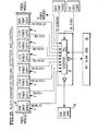
- FIG. 5 is a basic block diagram of the power control network showing the central power net master logic unit connected to control various power net slave logic units in this system.
- FIG. 6 is a block diagram showing the interconnection between the master logic unit and the slave logic units in the system.
- FIG. 7 is a block diagram of a typical power slave logic unit.
- FIG. 8 is a block diagram of the master network power logic unit showing the interconnections to the other parts of the system network.
- FIG. 9 is a block diagram of the peripheral power slave logic unit showing its connection to a peripheral cabinet and to the power control network of FIG. 5.
- FIG. 10 is a schematic diagram showing the protocol used for communication between master and slave units and additionally the byte format used.
- FIG. 11 is a flow diagram which summarizes the protocol activity for the master power network logic unit.
- FIG. 12 is a flow diagram which summarizes the protocol activity of the slave power control logic unit.
- FIG. 13 is an illustration showing the output signals from the slave logic to the power control circuit.
- FIG. 14 is an illustration showing the input signals from the power control circuit to the slave logic unit.
- FIG. 15 shows a block diagram illustrating the circuitry for failure detection and power control.
- FIG. 16 is a block diagram illustrating the circuitry for margin control voltages in local and remote modes.
- This subsystem relates to a computer network and system which interconnects the following type of cabinets:
- a “dependently-powered” cabinet is a cabinet which derives its AC power and its high voltage input DC power from another cabinet (other than itself) -- in this case the other cabinet is called the "processor cabinet". Thus, the "dependently-powered" cabinet must be physically attached to the source cabinet.
- An "independently-powered" cabinet is a cabinet which has its own AC power Source. It may, therefore, be considered as a "free-standing" unit.
- FIG. 1 indicates a block diagram of the network power control subsystem 10. Shown therein are a dependent power I/O cabinet 20 and 30, in addition to two processor cabinets 40 and 50. Additionally connected to the power control network are the independent power I/O cabinets 60 and 70.
- FIG. 2 shows the power components of processor cabinets 40 and 50 which were shown in FIG. 1.
- the power energization of the processor cabinets 40 and 50 is controlled by the power control card 80 shown in FIG. 2.
- the power control card 80 is controlled by a "system operator" through the cabinet control circuits via an "operator panel” 44, and by the operating maintenance personnel who work through the control display 45 (maintenance switches and indicators) within the processor cabinet.
- the power control card 80 additionally monitors the cabinet environmental conditions such as over-temperature and cooling air-loss. This card is further described later under the title of "Power Control Subsystem".
- the state of the cabinet power is further controlled by the power control network (PCN) through a card called the Power Net Slave Card 90.
- the processor cabinet (40, 50) also provides an AC power module 41 and a DC power module 43 for providing a high voltage DC to the attached-dependently-powered cabinets such as 20, 30.
- FIG. 3 illustrates the power components involved in the "dependently-powered” cabinets such as 20 and 30 of FIG. 1.
- the power for these "dependently-powered” cabinets is controlled by the power control card 80 d .
- This power control card 80 d is controlled by a system operator (operating technician) through the cabinet control circuits and operator panel 44 d , and also by the operating maintenance personnel through the control display 45 d (via maintenance switches and indicators) inside the cabinet.
- the power control card 80 d also is used to monitor the cabinet environmental conditions such as over-temperature and the cooling air-loss.
- the power in the dependently powered I/O cabinet of FIG. 3 is also controlled by the power control network through the power net slave card 90 d .
- the "dependently-powered" I/O cabinet (such as 20 and 30) receive their AC and their high voltage DC input voltage from the attached processor cabinets such as 40 and 50 of FIG. 1.
- FIG. 4 there is shown a block diagram of the various power components of the "independently-powered" cabinets such as 60 and 70 of FIG. 1.
- the power for these independently-powered cabinets is controlled by the power control card 80 i .
- the power control card 80 i is controlled by a "system operator” through the cabinet control circuits and operator panel 44 i ; and also by the operating maintenance personnel through the control display 45 i (via maintenance switches and indicators inside the cabinet).
- the power control card 80 i also monitors the environmental conditions in the cabinet such as over-temperature or the loss of "air”.
- the cabinet power of the independently-powered cabinet of FIG. 4 is also controlled by the power control network through the power net slave card 90 i .
- the "independently-powered" I/O cabinets contain two I/O backplanes which are referred to as backplane A, 70 a , and also backplane B, 70 b , in addition to two interface panels described hereinafter.
- the DC power to each backplane is separately controlled.
- the DC power to both interface panels will be supplied the same as on backplane A, 70 a .
- the operator panel 44 i will provide separate controls for each backplane.
- the power control network (PCN) will also provide separate controls for each of the backplanes 70 a and 70 b .
- each backplane The DC power to each backplane is controlled separately.
- the operator panel 44 i will provide separate controls for each backplane and also the power control network connections 95 n shown in FIG. 4 will provide separate controls for each backplane.
- the independently-powered cabinets will have their own AC power source and therefore may be considered as "free standing”.
- the "independently-powered" memory cabinet may provide a remote support interface adapter. This adapter adds the power net master logic card to the cabinet as discussed hereinafter.
- PCN Power Control Network
- a Power Control Network (PCN, FIGS. 1 and 5, via 95 n ) connects all system cabinets. This allows a "SINGLE-POINT" of on-site operator control of the entire system of many cabinets. That is, the on-site operator need only depress a single power-on or power-off switch to control the entire system.
- the PCN provides total "power control" from an external remote support center 300 via telephone connection.
- the integrated PCN system only a single remote connection is needed to drive the entire system.
- the PCN provides a number of system failures and status monitoring functions and system maintenance controls. These functions are described in paragraphs that follow.
- the PCN allows the capability for an UNATTENDED site, that is, no local system operator is required. All system power controls, failure condition monitoring, and maintenance controls are available via the PCN to the remote center, 300.
- the PCN is specifically implemented through power net slave cards contained in each system cabinet and interconnected to the PCN.
- Each slave card is "always" powered, that is, is powered if the AC breaker for its cabinet is on.
- the slave within a cabinet is powered whether the cabinet operating DC power is on or not.
- the power net master logic card 100 of FIG. 8, which is part of the before mentioned remote support interface adapter (contained within an independently-powered memory cabinet), drives the Power Control Network and therefore all the power net slaves.
- the master logic unit 100 provides the central hub between the power control functions (Power Control Network), the remote support center (300) telephone connection and the system maintenance (200, FIG. 8) subsystem.
- the master card 100 is also "always" powered.
- the Operator Control Panels 44, 44 d , 44 i , FIGS. 2, 3, 4, are accessible to the operator on the outside of the respective cabinets.
- the panels provide the following functions:
- the cabinet power control circuitry controls and monitors all the power modules of the various cabinets. It also monitors the various cabinet environmental conditions such as over-temperature, etc.
- the power control circuitry of the network system can be controlled from three sources:
- the operator panel control switches, in element 44, are active only when the cabinet is in the "cabinet mode" with the exception of the processor's power-on/power-off functions, and the cabinet/system switch. Table I indicates the switches for both the cabinet mode or system mode.
- the maintenance switches are active only when the cabinet is in the "cabinet mode".
- the power control network drive functions (the switch type functions) are active only when the cabinet is in the "system mode".
- the power control network monitor functions (that is the status) are always valid.
- the power state of the cabinet will follow the external power control signals derived from the slave units, as 90, 90 d , 90 i , etc.
- control display 45 (FIGS. 2, 3, 4) within a cabinet:
- PCN commands are actions to a cabinet driven by the PCN.
- PCN commands can only affect a cabinet when it is in "system” mode, described in paragraph A above.
- PCN status is information about the cabinet returned over the PCN.
- PCN status is available in either "system” or "cabinet" local modes.
- the PCN functions are selected separately for each backplane.
- the PCN (Power Control Network) functions are:
- the PCN shown in FIGS. 5 and 6 is serially routed, two-wire, twisted-pair.
- the PCN circuit uses R5422 standard differential drivers and receivers (FIG. 6).
- Connected on the PCN will be numerous power net slaves and peripheral slaves and one power net master.
- the total number of connections is 64.
- the maximum transfer rate may reach 10k bits/second.
- FIG. 6 shows the connection of the RS422 drivers and receivers for slave cards and the master card. Also shown is the network termination resistors of 120 and 470 ohms.
- Each slave and master card provides two PCN (Power Control Network) connectors.
- PCN Power Control Network
- One connector receives the PCN cable from the previous unit and the other connector sends the PCN cable to the next unit. The PCN is thus serially routed.
- the PCN cable is a simple, inexpensive, twisted-pair cable.
- the PCN cables For PCN connections to non-attached cabinets, the PCN cables first are routed through interface panel cards in an I/O cabinet through RFI shielded cable into the non-attached cabinet.
- FIG. 7 shows a block diagram for a power net slave card.
- the diagram shows the controlling microprocessor 92 and the address switches 94 which give each cabinet an unique PCN address.
- Each slave has two parallel connecting ports 96, 97 to the power control cards of its cabinet.
- the slave also provides, via circuit 98, clock select or other signals and connects the RS422 interface to the PCN network itself.
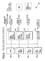
- FIG. 8 shows the power net master logic unit 100 card block diagram
- FIG. 9 shows a peripheral-slave card block diagram. This slave can control only the power-on and power-off of a peripheral cabinet (disk pack controller).
- the power network slave logic shows a logic card connected between the power control circuits of a cabinet and the power control network.
- a major element of the slave logic card is a microprocessor such as an 8748 chip which contains internal program PROM and internal RAM.
- a typical chip of this designation is manufactured by Intel Corporation, whose address is 3065 Bowers Avenue, Santa Clara, California, and wherein this chip is described in a publication entitled "Microcontroller User's Manual", Order #210359-001, copyright 1982, and published by Intel Corporation, Literature Dept. SU3-3, of 3065 Bowers Avenue, Santa Clara, California.
- Each slave logic unit has a unique address which is set within the card by means of switches shown as element 94, address switches, in FIG. 7.
- the slave logic is connected to the power control network of FIG. 5 using the circuits shown in FIG. 6, which are RS422 receiver and driver chips.
- the RS422 receiver and driver chips are those such as typically manufactured by Advanced Micro Devices Company of 901 Thompson Place, (P.O. Box 453), Sunnyvale, California. These circuits are described in a publication entitled "Bipolar Microprocessor Logic & Interface Data Book" published by Advanced Micro Devices Company, copyright 1983.
- the power network slave logic in FIG. 7 has two ports designated as port A interface 96 and port B interface 97. These interfaces connect to the power control circuits within each of the cabinets such, for example, as power control card 80 of FIG. 2, power control card 80 d of FIG. 3, and power control card 80 i of FIG. 4.
- the signals to and from the port A96 and port B97 are described hereinafter.
- the power network slave logic unit 90 has four output signals (shown in FIG. 7 at the extreme right side) which may be activated or deactivated under the control of commands sent over the power control network. Thus, these four output signals may be used in cabinets containing a DPM (dual port memory) , or for independent memory cabinets, in order to select the source for the DPM clocks. These four signals are individually controlled, raised or lowered, by commands from over the power net from the power net master logic unit 100 of FIG. 5.
- DPM dual port memory
- TTL transistor type logic
- the Select Circuits 98 of FIG. 7 use the inverter-buffer chips to provide a signal from the slave logic over a coaxial cable over to the DPM (Dual Port Memory) back plane.
- the power network slave logic unit 90 requires the use of control signals or "always power" from the cabinet in which it resides.
- Two on-board indicators and one switch are used to control each of the power network slave logic units 90, 90 i , 90 d , 90 p .
- a push-button switch (the re-set switch) is used to initialize the slave logic to run its own “self-test”. This is the same function that occurs at slave power-up time.
- One indicator (self-test) is "on” when the slave self-test program is in operation. If a self-test error occurs, this indicator will remain "on”.
- the second indicator (NET ERROR) is "on” whenever the slave logic detects a "NET" problem while the slave is communicating on "NET".
- NET errors include a framing error (too few or too many discs), a parity error, a NET protocol error, and an invalid command.
- the "NET ERROR” indicator will be deactivated when a "good" net communication to the slave logic unit occurs.
- FIG. 8 A block diagram of the power network master logic is shown in FIG. 8.
- the power network master logic 100 of FIG. 8 is housed in an independently-powered memory cabinet within the system, such as cabinet 70 of FIG. 1.
- the power network master logic will require power from this cabinet.
- the master logic 100 is the controlling device on the power control network of FIG. 5. It initiates all communications over the network; and thus, all communications over the network are effectuated between the master 100 and a slave logic unit such as 90. There is only one "active" master logic unit, such as 100, which may be connected to the power control network of FIG. 5 at any given time.
- the network master logic 100 also interfaces to the Maintenance Subsystem (200 shown in FIG. 8) through the System Control Network shown in FIG. 5. Also, as indicated in FIG. 5, the power network master logic is the single point of connection of the system to a Remote Support Center (RSC, 300 in FIGS. 5 and 8).
- RSC Remote Support Center
- FIG. 8 also shows the connections to the Remote Support Center 300 and also to the power control network of FIG. 5.
- the power network master logic unit 100 is provided with a microprocessor 100 u to which are connected a PROM 100 ml and EEPROM 100 m2 in addition to a RAM unit 100 a .
- a power control interface 100 p connects the microprocessor to the power control network and a remote support interface 100 r connects the microprocessor to the remote support center 300.
- a time of day circuit 100 t with battery back-up provides time signals for the unit.
- the power network master logic unit 100 of FIG. 8 provides a central interconnection point for the power control network of FIG. 5, in addition to the system control network which is connected through the interface 100 s . It is also the central interconnection point for the remote support center interface (remote diagnostic) of element 100 r .
- the power network master logic unit 100 as the master unit for the power network, controls all the actions on this network.
- any multi-processor system there may be only one "active" power network master logic unit. Since, however, this unit is of considerable importance to the system operation and maintenance, there is generally provided a spare power network master logic unit, even though a failure in the power subsystem will not affect the operation of the overall processing unit.
- the microprocessor 100 u (Intel 8088) of FIG. 8 may be set to run at 8 megahertz. It executes its code out of the 32 K bytes of PROM 100 ml .
- the 8 K bytes of RAM 100 a are used for data buffers and for operating stacks.
- the 256 bytes of electrically erasable PROM 100 m2 are used to store configuration-dependent option flags.
- the time of day circuit 100 t is backed up by a battery for use during times of power failure. Six indicators and five switches are provided on the master logic unit 100 for maintenance of the master card itself.
- Peripheral Slave Power Control Adaptor Peripheral Slave Power Control Adaptor
- the power control network may include peripheral devices which are provided with a peripheral slave power control adaptor 90 p .
- FIG. 9 shows a block diagram of such a peripheral slave power control adaptor 90 p .
- a microprocessor 92 p which connects to a peripheral power control driver circuit 95 p having connections to the peripheral cabinet.
- address switches 94 p which provide an input to the microprocessor 92 p , and also a driver-receiver circuit 99 p which connects to the power control network of FIG. 5.
- the peripheral slave power control adaptor such as 90 p of FIG. 9, is located in an interface panel within the I/O cabinets such as 60 and 70 of FIG. 1, and also in cabinets 20 and 30 of FIG. 1.
- the peripheral slave power control adaptor 90 p of FIG. 9 connects between the power control network of FIG. 5 and any selected system peripheral cabinets. There are certain cabinet types to which the peripheral slave power control adaptor may be connected. These are:
- the peripheral slave adaptor 90 p provides only "power-on” and “power-off” control for these cabinets.
- the peripheral slave adaptor 90 p is logically a simple slave unit.
- the microprocessor 92 p may use an 8748 microprocessor chip (previously described) and interfaces to the power control network with the RS422 driver receiver chip designated 99 p .
- the peripheral slave logic of FIG. 9 differs from the internal power slave logic unit of FIG. 7 in that, in place of the port A and port B interfaces (96, 97) of FIG. 7, the "peripheral" slave logic has special driver circuits 95 p in order to control the "on/off" state of the connecting peripheral cabinets.
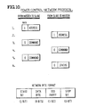
- FIG. 10 is an illustrative drawing showing the particular sequence of events over the network.
- the master logic unit 100 first sends the Address byte shown in line 1 of the drawing of FIG. 10. This Address is the address of the desired slave unit to be addressed. Each slave unit receives and evaluates the Address received and then the appropriate slave unit will return its Address to the master power unit 100.
- the master logic unit 100 will send a Command byte (shown in line 3) to the previously addressed slave unit, such as 90 of FIG. 7.
- the slave unit such as 90, then returns the Command byte to the master as illustrated in line 4 of FIG. 10.
- the slave has received the Command byte, it returns it to the master and if the byte received by the master logic unit 100 then agrees with the byte that it (master unit) had previously sent, the master logic unit 100 re-sends the Command byte again, as illustrated in line 5 showing the Command byte being re-sent from master to slave.
- the slave logic unit 90 will decode and execute the Command received. The slave will then return its General Status byte to the master as seen in line 6 of FIG. 10.
- the specified Status byte is returned instead of the General Status byte.
- the General Status byte which is returned to the slave logic unit 90 will not reflect the new power state of the cabinet involved. It will show the status of the cabinet "prior to" the command. To check the new state of the cabinet involved, a Send Status Command will be sent about 15 seconds later after the power on/off Command was sent.
- FIG. 10 indicates the general network flow for the master power logic unit 100 as it polls the various slaves 90 over the network. After the master logic unit 100 sends an Address, it waits for the return of the addressed slave unit's address. If an incorrect address is returned from the slave logic unit 90, the master power logic unit 100 will re-try the expected address. It will try the desired address three times before it assumes that the Address slave logic unit 90 may be "bad".
- the master power logic unit 100 also does the same re-try/time-out procedures for the Command bytes.
- the master power logic unit 100 finds an "improperly" responding slave logic unit 90, while polling, it will report the condition to the maintenance subsystem 200 over the system control network connected as shown in FIG. 8.
- FIG. 10 also indicates the network byte format for the power network. As shown therein, there is one bit used for a start bit, then 8 bits are used for a data byte, then one bit is used for odd parity, and one bit is used as a stop bit.
- FIG. 11 shows a drawing of a flow chart showing the network flow for the master power control logic unit 100 which summarizes the various protocol steps used in FIG. 10 on lines 1-6.
- FIG. 12 is a flow chart diagram which summarizes the protocol involved for the slave power logic unit in the system operation.
- Table II shows one scheme on which Addresses may be provided for the processor cabinets, the independent memory cabinets, the I/O cabinets, and the various peripheral cabinets, whereby the power control network system may address and communicate with specific cabinets in order to provide Command and Control functions in the power network system.
- the PCN Since the PCN has "great power" over a system, that is, it can turn off a system, it is necessary that the network protocol be fault tolerant and reliable.
- the PCN protocol was designed with several layers of redundancy and checking.
- FIG. 10 shows the PCN byte format.
- the PCN byte contains one start bit, eight bits of information (data byte), one odd-parity bit, and one stop bit.
- FIG. 10 also shows the PCN message transfer protocol between the power net master card and a slave card. All transfers on the PCN are initiated by the master. All transactions follow the steps described below:
- FIG. 11 gives the master flow (less steps a - d).
- FIG. 12 gives the slave flow.
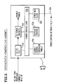
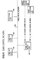
- the power control subsystem shown in FIGS. 13, 14, 15 and 16 is used to controllably sequence various power supply modules either “on” or “off” and to detect failures in the power modules or cooling systems that could damage the logic cards, interfaces or memory storage devices.
- the power sequence control and failure detection is oriented around the power control circuit card 80 (80 i , 80 d ) in conjunction with its interface to the slave logic units 90 (90 i , 90 d ) as shown in FIGS. 13 and 14.
- FIG. 13 shows the output control signals from the slave logic 90 to the power control circuit 80.
- FIG. 14 shows the various "indicator" signals which the power control circuit provides to the slave logic 90.
- TTL transistor type logic
- Each power supply module (as 41, 43, 70 a , 70 b , of FIGS. 2, 3, 4) will send a TTL signal back to the power control circuit 80 (80 i , 80 d ) to indicate if that module failed or was under voltage, over voltage, over current or over temperature.
- the over temperature or air loss sensors of FIG. 15 can send failure signals to the sequencer 80 q in power control circuit 80.
- a precision reference voltage unit 80 r has programmable voltage steps of + (plus) or - (minus) 5 percent which can be controlled by input signals via a local interface from margin switches 80 s , or via a remote interface from slave logic 90. This permits "margining" of the output voltages on each power supply module.
- Each power supply module has a + 5V reference supplied by reference unit 80 r which controls the output voltage of each power module, and any change in reference voltage causes a proportional change in output voltage.
- the precision + 5V reference voltage has two programmable inputs for effecting + 5% and - 5% voltage change steps.
- the margin steps can be activated "locally” by a switch or "remotely” by the slave logic 90.
- Each logic power module has its own separate reference voltage and margin circuit.
- the main AC power module (such as the 15KW input module 41 of FIG. 15) can be set on or off via a TTL signal "S" from the power control circuit 80.
- the cabinet control panel 44 (FIGS. 2, 15) enables "local mode” operation by a technician or system operator, and has an on/off push button with light-indicator, with power-failure/temperature-failure indicator and local/remote switch with indicator light.
- the two modes ford controlling power on/off are the "local” mode and the "remote” mode.
- the local mode requires an "on-site" operator to manually start the power control on/off responses by use of an ON/OFF switch on cabinet control panel 44.
- the remote mode allows the "system control" in the network whereby the master logic 100 (FIG. 8) instructs the appropriate slave logic 90 to command certain actions to its power control circuit 80.
- the local/remote keyswitch in the cabinet control panel 44 enables or disables the local/remote interface (FIG. 16) in the power control circuit 80. Then depending on what mode the system is in, the sequencer 80 q turns each power supply module on/off in the appropriate sequential order.
- each power module can furnish a TTL compatible "fail" signal to the sequencer 80 p in the power control circuit 80.
- the power sequencer 80 q is a circuit which ensures that the main power module 41 is operating before checking the subordinate power modules, after which any incoming failure signal which is detected will make the sequencer shut off all the power modules in that subsystem.
- the sequencer 80 q will also signal the slave logic 90 with a TTL compatible signal. Any failures are also indicated by light-emitting diodes which make reference to each power module. A similar failure indicator on the cabinet control panel 44 is also turned on.
Landscapes
- Engineering & Computer Science (AREA)
- Theoretical Computer Science (AREA)
- General Engineering & Computer Science (AREA)
- Physics & Mathematics (AREA)
- General Physics & Mathematics (AREA)
- Computer Hardware Design (AREA)
- Computing Systems (AREA)
- Power Sources (AREA)
Claims (7)
- Spannungssteuerungsnetzwerk zur Steuerung des Spannungszustands von ausgewählten Modulen in einem System von miteinander verbundenen Modulen, die mindestens ein Prozessormodul, mindestens ein E/A-Modul und mindestens ein Speichermodul umfassen und bei denen jedes Modul eine interne Spannungsteuerungsschalteinrichtung (80) und eine interne Spannungsversorgungseinrichtung enthält, wobei das Spannungssteuerungsnetzwerk aufweist:a) eine Master-Logikspannungseinheiteinrichtung (100) zur Messung des Spannungszustands von jedem Modul und zur Übertragung von Steuerbefehlen zur Regulierung des Ein/Aus-Spannungszustands eines ausgewählten Moduls oder von Modulen oder allen Modulen;b) eine Slave-Logikspannungseinheiteinrichtung für den Empfang der Steuerbefehle und für die Regulierung des Spannungszustandes von jedem Modul, wobei die Slave-Logikspannungseinheiteinrichtung aufweist:(b1) mehrere Slave-Logikeinheiten (90), von denen jede mit der Master-Logikeinheiteinrichtung (100) verbunden ist und bei denen jedes Modul mit einer einzelnen in diesem befindlichen Slave-Einheit (90) versehen ist;(b2) wobei die Spannungssteuerschalteinrichtung (80) unter den Steuerbefehlen von der Master-Einheit (100) über die Slave-Einheit (90) arbeitet, um die Spannung in dem Modul, in dem sich die Slave-Einheit befindet, ein- oder abzuschalten;dadurch gekennzeichnet, daß
die Spannungsteuerungsschalteinrichtung (80)(b2a) eine Einrichtung (80s) aufweist, die eine Erhöhung oder Verringerung des Ausgangs der internen Spannungsversorgungseinrichtung um einen festen Prozent-Betrag veranlaßt. - Spannungsteuerungsnetzwerk nach Anspruch 1, bei welchem jede Slave-Logikeinheit (90)(a) eine Einrichtung (80g) aufweist, um den Spannungszustand der internen Spannungsversorgungseinrichtung zu messen, die sich in demselben Modul wie die Slave-Logikeinheit (90) befindet.
- Spannungsteuerungsnetzwerk nach Anspruch 1 oder 2, bei welchem die Master-Logikspannungseinheiteinrichtung (100) aufweist:(a) eine Master-Microprozessoreinrichtung (100µ) zur Ausführung von Programmbefehlen, um die interne Spannungsversorgungseinrichtung in einem ausgewählten Modul heraus- oder herunterzufahren;(b) eine mit der Master-Microprozessoreinrichtung (100µ) verbundene Speichereinrichtung (100m₁, 100a, 100m₂) zur Programmspeicherung und Datenpufferung;(c) eine mit der Microprozessoreinrichtung (100µ) verbundene Interfaceeinrichtung (100p) zur Durchführung von Datenübertragungen an jede und von jeder Slave-Logikeinheit (90); und(d) eine Tageszeiteinrichtung (100t) zur Übermittlung von Zeitsignalen an die Master-Microprozessoreinrichtung (100µ), um ein unbeaufsichtigtes Hochfahren des Systems und eine Haltelast zu ermöglichen und den Zeitpunkt eines Fehlers der Einheit aufzuzeichnen.
- Spannungssteuerungsnetzwerk nach Anspruch 3, bei welchem die Master-Microprozessoreinrichtung (100µ) außerdem(a) eine Einrichtung enthält, um Befehle an eine Slave-Logikeinheit (90) zur Erhöhung/Absenkung der Spannungswerte um einen festen Betrag zu übermitteln.
- Spannungssteuerungsnetzwerk nach einem der Ansprüche 1 bis 4, bei welchem jede Slave-Logikeinheit (90) aufweist:(a) eine Slave-Microprozessoreinrichtung (92) für den Empfang und die Ausführung von Befehlen von der Master-Spannungslogikeinheit (100) und für die Übertragung der Spannungszustandsinformationsdaten an die Master-Logikeinheit (100);(b) eine Adressenschalteinrichtung zur Erzeugung einer einheitlichen Adresse, um jede Spannungs-Slave-Logikeinheit zu identifizieren, wobei die Schalteinrichtung an die Slave-Microprozessoreinrichtung (92) angeschlossen ist;(c) einen Kommunikationsübertragungsschaltkreis zur Übertragung von Befehlen und Daten zwischen den Slave-Microprozessoreinrichtungen und den Master-Logikeinheiten (100) und(d) einen Interfaceschaltkreis (96, 97) zum Anschluß der Slave-Microprozessoreinrichtungen (92) an die Spannungssteuerungsschalteinrichtungen in den Modulen, um den Ein/Aus-Zustand der Spannung in jedem Modul zu steuern.
- Spannungsteuerungsnetzwerk nach Anspruch 5, bei welchem die Slave-Microprozessoreinrichtung (92)(a) eine Einrichtung für die Ausführung von Befehlen zum Erhöhen/Absenken der Spannung der internen Spannungsversorgungseinrichtung enthält.
- Spannungssteuerungsnetzwerk nach Anspruch 6, bei welchem jede Slave-Logikeinheit (90)(a) einen Speichertaktauswahlschaltkreis (98) enthält, der angeschlossen ist, um Taktsignale von der Slave-Microprozessoreinrichtung (92) zu empfangen und ein Taktauswahlsignal an das Speichermodul zu übermitteln.
Applications Claiming Priority (2)
| Application Number | Priority Date | Filing Date | Title |
|---|---|---|---|
| US06/662,477 US4677566A (en) | 1984-10-18 | 1984-10-18 | Power control network for multiple digital modules |
| US662477 | 1991-02-27 |
Publications (3)
| Publication Number | Publication Date |
|---|---|
| EP0178642A2 EP0178642A2 (de) | 1986-04-23 |
| EP0178642A3 EP0178642A3 (en) | 1988-03-30 |
| EP0178642B1 true EP0178642B1 (de) | 1991-07-24 |
Family
ID=24657887
Family Applications (1)
| Application Number | Title | Priority Date | Filing Date |
|---|---|---|---|
| EP85113110A Expired - Lifetime EP0178642B1 (de) | 1984-10-18 | 1985-10-16 | Netzwerk zur Steuerung der Spannungsversorgung von mehreren Digitalmodulen |
Country Status (5)
| Country | Link |
|---|---|
| US (1) | US4677566A (de) |
| EP (1) | EP0178642B1 (de) |
| JP (1) | JPS61114322A (de) |
| CA (1) | CA1246235A (de) |
| DE (1) | DE3583574D1 (de) |
Families Citing this family (85)
| Publication number | Priority date | Publication date | Assignee | Title |
|---|---|---|---|---|
| US5274797A (en) * | 1986-05-30 | 1993-12-28 | Bull Hn Information Systems Inc. | Multiprocessor system with centralized initialization, testing and monitoring of the system and providing centralized timing |
| WO1988008580A1 (en) * | 1987-05-01 | 1988-11-03 | Digital Equipment Corporation | Backplane bus |
| US5003467A (en) * | 1987-05-01 | 1991-03-26 | Digital Equipment Corporation | Node adapted for backplane bus with default control |
| US4837736A (en) * | 1987-05-01 | 1989-06-06 | Digital Equipment Corporation | Backplane bus with default control |
| EP0357667B1 (de) * | 1987-05-01 | 1993-07-21 | Digital Equipment Corporation | Knoten für rückwandplatinenbus |
| JP2760787B2 (ja) * | 1987-08-28 | 1998-06-04 | 株式会社日立製作所 | 電子計算機システムの運転制御装置 |
| JPH0650457B2 (ja) * | 1987-10-14 | 1994-06-29 | シャープ株式会社 | コンピュータシステムのデバイス電源制御装置 |
| ATA189988A (de) * | 1988-07-25 | 1994-08-15 | Philips Nv | Elektronische baugruppen aufweisendes system mit mindestens einem mikroprozessor |
| JP2694993B2 (ja) * | 1989-02-22 | 1997-12-24 | 株式会社日立製作所 | 電力用信号処理システムおよびディジタル保護リレー装置 |
| JP2761924B2 (ja) * | 1989-06-08 | 1998-06-04 | キヤノン株式会社 | ユニット間通信装置 |
| US5142684A (en) * | 1989-06-23 | 1992-08-25 | Hand Held Products, Inc. | Power conservation in microprocessor controlled devices |
| ATE121208T1 (de) * | 1990-01-30 | 1995-04-15 | Johnson Service Co | Vernetztes betriebsmittelverwaltungssystem. |
| US5396635A (en) * | 1990-06-01 | 1995-03-07 | Vadem Corporation | Power conservation apparatus having multiple power reduction levels dependent upon the activity of the computer system |
| US5742514A (en) * | 1992-10-20 | 1998-04-21 | Compaq Computer Corporation | Integrated remote asynchronous power switch |
| US5483656A (en) * | 1993-01-14 | 1996-01-09 | Apple Computer, Inc. | System for managing power consumption of devices coupled to a common bus |
| KR950005216B1 (ko) * | 1993-03-31 | 1995-05-22 | 삼성전자주식회사 | 컴퓨터 주변장치의 전원절약장치 |
| US5535401A (en) * | 1994-04-05 | 1996-07-09 | International Business Machines Corporation | Method and system of power and thermal management for a data processing system using object-oriented program design |
| US5537462A (en) * | 1994-04-15 | 1996-07-16 | Aegis Technologies, Inc. | Supervisory interface controller and method for remotely controlled terminal |
| US5652893A (en) * | 1994-12-13 | 1997-07-29 | 3Com Corporation | Switching hub intelligent power management |
| AU4519596A (en) * | 1994-12-22 | 1996-07-10 | Intel Corporation | Power budgeting with device specific characterization of power consumption |
| JPH08202468A (ja) * | 1995-01-27 | 1996-08-09 | Hitachi Ltd | マルチプロセッサシステム |
| US5958056A (en) * | 1995-05-26 | 1999-09-28 | Intel Corporation | Method and apparatus for selecting operating voltages in a backplane bus |
| US5809313A (en) * | 1995-07-06 | 1998-09-15 | Sun Microsystems, Inc. | Method and apparatus for powering-on a computer-based system via a network interface |
| DE19614237C1 (de) * | 1996-04-10 | 1997-12-11 | Siemens Ag | Kommunikationssystem mit einer Meisterstation und mindestens einer Sklavenstation |
| JP3145942B2 (ja) * | 1997-02-18 | 2001-03-12 | 日本電気株式会社 | 電源システム |
| US6125448A (en) * | 1997-05-02 | 2000-09-26 | 3Com Corporation | Power subsystem for a communication network containing a power bus |
| KR100262518B1 (ko) * | 1997-07-09 | 2000-08-01 | 윤종용 | 시스템상태를감지할수있는전원분배유닛 |
| DE69904875T2 (de) * | 1998-06-01 | 2003-08-28 | Seiko Epson Corp | Verfahren zur Überwachung des Stromversorgungszustands in einem an einen Hauptrechner angeschlossenen Peripheriegerät |
| JP4403331B2 (ja) * | 2000-02-22 | 2010-01-27 | ソニー株式会社 | 電子機器システム、情報処理機器 |
| US7249043B1 (en) | 2000-03-10 | 2007-07-24 | E.P.M., Inc. | Computer program and method for reducing HVAC demand for energy |
| US6701442B1 (en) | 2000-05-09 | 2004-03-02 | 3Com Corporation | Power management circuit for selectively applying power to network monitoring circuitry which monitors the receipt of network wake-up messages |
| GB2364867B (en) * | 2000-07-17 | 2003-12-10 | Advanced Risc Mach Ltd | A data processing apparatus and slave interface mechanism for controlling access to a slave logic unit by a plurality of master logic units |
| US20070245165A1 (en) * | 2000-09-27 | 2007-10-18 | Amphus, Inc. | System and method for activity or event based dynamic energy conserving server reconfiguration |
| USRE40866E1 (en) | 2000-09-27 | 2009-08-04 | Huron Ip Llc | System, method, and architecture for dynamic server power management and dynamic workload management for multiserver environment |
| US7822967B2 (en) | 2000-09-27 | 2010-10-26 | Huron Ip Llc | Apparatus, architecture, and method for integrated modular server system providing dynamically power-managed and work-load managed network devices |
| US7058826B2 (en) | 2000-09-27 | 2006-06-06 | Amphus, Inc. | System, architecture, and method for logical server and other network devices in a dynamically configurable multi-server network environment |
| US7032119B2 (en) | 2000-09-27 | 2006-04-18 | Amphus, Inc. | Dynamic power and workload management for multi-server system |
| US7228441B2 (en) * | 2000-09-27 | 2007-06-05 | Huron Ip Llc | Multi-server and multi-CPU power management system and method |
| US20030196126A1 (en) * | 2002-04-11 | 2003-10-16 | Fung Henry T. | System, method, and architecture for dynamic server power management and dynamic workload management for multi-server environment |
| US20060248360A1 (en) * | 2001-05-18 | 2006-11-02 | Fung Henry T | Multi-server and multi-CPU power management system and method |
| US6915440B2 (en) * | 2001-06-12 | 2005-07-05 | International Business Machines Corporation | Apparatus, program product and method of performing power fault analysis in a computer system |
| US6653816B2 (en) | 2001-06-24 | 2003-11-25 | Motorola, Inc. | Battery with embedded power management |
| US7203852B2 (en) * | 2001-06-29 | 2007-04-10 | Intel Corporation | System and process for making power readily available to newly added computers |
| US6948079B2 (en) * | 2001-12-26 | 2005-09-20 | Intel Corporation | Method and apparatus for providing supply voltages for a processor |
| US20030126477A1 (en) * | 2001-12-28 | 2003-07-03 | Zhang Kevin X. | Method and apparatus for controlling a supply voltage to a processor |
| EP1474753B1 (de) * | 2002-02-15 | 2018-08-22 | Tridium, Inc. | Komponentenmodell für die echtzeit-systemsteuerung |
| US7394445B2 (en) * | 2002-11-12 | 2008-07-01 | Power-One, Inc. | Digital power manager for controlling and monitoring an array of point-of-load regulators |
| US6949916B2 (en) | 2002-11-12 | 2005-09-27 | Power-One Limited | System and method for controlling a point-of-load regulator |
| US7456617B2 (en) * | 2002-11-13 | 2008-11-25 | Power-One, Inc. | System for controlling and monitoring an array of point-of-load regulators by a host |
| US6833691B2 (en) * | 2002-11-19 | 2004-12-21 | Power-One Limited | System and method for providing digital pulse width modulation |
| US7737961B2 (en) * | 2002-12-21 | 2010-06-15 | Power-One, Inc. | Method and system for controlling and monitoring an array of point-of-load regulators |
| US7266709B2 (en) * | 2002-12-21 | 2007-09-04 | Power-One, Inc. | Method and system for controlling an array of point-of-load regulators and auxiliary devices |
| US7882372B2 (en) * | 2002-12-21 | 2011-02-01 | Power-One, Inc. | Method and system for controlling and monitoring an array of point-of-load regulators |
| US7743266B2 (en) * | 2002-12-21 | 2010-06-22 | Power-One, Inc. | Method and system for optimizing filter compensation coefficients for a digital power control system |
| US7673157B2 (en) | 2002-12-21 | 2010-03-02 | Power-One, Inc. | Method and system for controlling a mixed array of point-of-load regulators through a bus translator |
| US7249267B2 (en) | 2002-12-21 | 2007-07-24 | Power-One, Inc. | Method and system for communicating filter compensation coefficients for a digital power control system |
| US7836322B2 (en) * | 2002-12-21 | 2010-11-16 | Power-One, Inc. | System for controlling an array of point-of-load regulators and auxiliary devices |
| US7373527B2 (en) * | 2002-12-23 | 2008-05-13 | Power-One, Inc. | System and method for interleaving point-of-load regulators |
| US7710092B2 (en) * | 2003-02-10 | 2010-05-04 | Power-One, Inc. | Self tracking ADC for digital power supply control systems |
| US7023190B2 (en) * | 2003-02-10 | 2006-04-04 | Power-One, Inc. | ADC transfer function providing improved dynamic regulation in a switched mode power supply |
| US6936999B2 (en) * | 2003-03-14 | 2005-08-30 | Power-One Limited | System and method for controlling output-timing parameters of power converters |
| US7080265B2 (en) * | 2003-03-14 | 2006-07-18 | Power-One, Inc. | Voltage set point control scheme |
| US7739523B2 (en) * | 2003-03-17 | 2010-06-15 | Canon Kabushiki Kaisha | Display system, access point of display system, and power control method |
| US7831282B2 (en) * | 2003-10-15 | 2010-11-09 | Eaton Corporation | Wireless node providing improved battery power consumption and system employing the same |
| US7372682B2 (en) * | 2004-02-12 | 2008-05-13 | Power-One, Inc. | System and method for managing fault in a power system |
| JP2005254621A (ja) * | 2004-03-11 | 2005-09-22 | Seiko Epson Corp | 電源制御装置及び電源制御方法 |
| US7346788B2 (en) * | 2004-06-04 | 2008-03-18 | Broadcom Corporation | Method and system for monitoring module power information in a communication device |
| US7900065B2 (en) * | 2004-06-04 | 2011-03-01 | Broadcom Corporation | Method and system for monitoring module power status in a communication device |
| US7554310B2 (en) * | 2005-03-18 | 2009-06-30 | Power-One, Inc. | Digital double-loop output voltage regulation |
| US7141956B2 (en) * | 2005-03-18 | 2006-11-28 | Power-One, Inc. | Digital output voltage regulation circuit having first control loop for high speed and second control loop for high accuracy |
| US7239115B2 (en) * | 2005-04-04 | 2007-07-03 | Power-One, Inc. | Digital pulse width modulation controller with preset filter coefficients |
| US7327149B2 (en) * | 2005-05-10 | 2008-02-05 | Power-One, Inc. | Bi-directional MOS current sense circuit |
| US7560913B2 (en) * | 2006-09-22 | 2009-07-14 | International Business Machines Corporation | Input-tracking, automatic output-margining method and system |
| US20090082880A1 (en) * | 2007-09-20 | 2009-03-26 | Tridium Inc. | Wireless device for a building control system |
| US7834613B2 (en) * | 2007-10-30 | 2010-11-16 | Power-One, Inc. | Isolated current to voltage, voltage to voltage converter |
| US8533528B2 (en) * | 2009-12-16 | 2013-09-10 | Hewlett-Packard Development Company, L.P. | Fault tolerant power sequencer |
| JP5457273B2 (ja) * | 2010-05-31 | 2014-04-02 | 富士通コンポーネント株式会社 | 電源制御システム、電源制御システムの制御方法、電源制御装置及びプログラム |
| WO2012003847A1 (en) | 2010-07-08 | 2012-01-12 | Nec Europe Ltd. | Method of supporting power control in a communication network |
| US9213397B2 (en) | 2012-09-21 | 2015-12-15 | Atmel Corporation | Changing power modes of a microcontroller system |
| US9213388B2 (en) | 2012-09-21 | 2015-12-15 | Atmel Corporation | Delaying reset signals in a microcontroller system |
| US9323312B2 (en) | 2012-09-21 | 2016-04-26 | Atmel Corporation | System and methods for delaying interrupts in a microcontroller system |
| US9507406B2 (en) | 2012-09-21 | 2016-11-29 | Atmel Corporation | Configuring power domains of a microcontroller system |
| US9383807B2 (en) * | 2013-10-01 | 2016-07-05 | Atmel Corporation | Configuring power domains of a microcontroller system |
| US9684367B2 (en) | 2014-06-26 | 2017-06-20 | Atmel Corporation | Power trace port for tracing states of power domains |
| EP3410243B1 (de) * | 2016-01-28 | 2020-10-14 | Fuji Corporation | Energieverwaltungssystem für eine produktionslinie |
Family Cites Families (16)
| Publication number | Priority date | Publication date | Assignee | Title |
|---|---|---|---|---|
| US3715729A (en) * | 1971-03-10 | 1973-02-06 | Ibm | Timing control for a multiprocessor system |
| US3736569A (en) * | 1971-10-13 | 1973-05-29 | Ibm | System for controlling power consumption in a computer |
| GB1536046A (en) * | 1976-06-30 | 1978-12-20 | Ibm | Data processing system power control |
| JPS5327322A (en) * | 1976-08-26 | 1978-03-14 | Fujitsu Ltd | Power supply control system |
| JPS5418238A (en) * | 1977-07-12 | 1979-02-10 | Toshiba Corp | Automatic power supply throw-in device |
| US4224684A (en) * | 1978-09-22 | 1980-09-23 | International Business Machines Corporation | Receive/bypass circuit for subsystems in polling system |
| US4213182A (en) * | 1978-12-06 | 1980-07-15 | General Electric Company | Programmable energy load controller system and methods |
| US4312035A (en) * | 1979-06-18 | 1982-01-19 | Greene Richard E | Apparatus for controlling electrical power in a data processing system |
| US4264960A (en) * | 1979-07-02 | 1981-04-28 | Sangamo Weston, Inc. | System for controlling power distribution to customer loads |
| US4316246A (en) * | 1979-09-06 | 1982-02-16 | Honeywell Information Systems Inc. | Battery switching apparatus included within a timer adapter unit |
| US4347576A (en) * | 1980-04-28 | 1982-08-31 | Honeywell Inc. | Load management control apparatus with improved duty cycle operation |
| FR2497373B1 (fr) * | 1980-12-30 | 1986-09-05 | Bull Sa | Systeme d'alimentation microprogrammable pour systeme de traitement de donnees comportant un panneau de service destine aux operations de maintenance et procedes d'exploitation de ce panneau de service |
| JPS582913A (ja) * | 1981-06-30 | 1983-01-08 | Fuji Electric Co Ltd | 高圧安定化電源 |
| JPS5814226A (ja) * | 1981-07-20 | 1983-01-27 | Usac Electronics Ind Co Ltd | 電子計算機の電源制御方式 |
| JPS58115508A (ja) * | 1981-12-29 | 1983-07-09 | Fujitsu Ltd | 電源制御装置 |
| US4589075A (en) * | 1983-02-23 | 1986-05-13 | Buennagel James A | Remote load data acquisition and control system for a power network |
-
1984
- 1984-10-18 US US06/662,477 patent/US4677566A/en not_active Expired - Lifetime
-
1985
- 1985-10-16 CA CA000493062A patent/CA1246235A/en not_active Expired
- 1985-10-16 EP EP85113110A patent/EP0178642B1/de not_active Expired - Lifetime
- 1985-10-16 DE DE8585113110T patent/DE3583574D1/de not_active Expired - Fee Related
- 1985-10-17 JP JP60233142A patent/JPS61114322A/ja active Granted
Also Published As
| Publication number | Publication date |
|---|---|
| JPS61114322A (ja) | 1986-06-02 |
| CA1246235A (en) | 1988-12-06 |
| EP0178642A2 (de) | 1986-04-23 |
| JPH0479005B2 (de) | 1992-12-14 |
| EP0178642A3 (en) | 1988-03-30 |
| DE3583574D1 (de) | 1991-08-29 |
| US4677566A (en) | 1987-06-30 |
Similar Documents
| Publication | Publication Date | Title |
|---|---|---|
| EP0178642B1 (de) | Netzwerk zur Steuerung der Spannungsversorgung von mehreren Digitalmodulen | |
| US4663539A (en) | Local power switching control subsystem | |
| EP0176342B1 (de) | Netzwerk zur Spannungsversorgungskontrolle mit betriebsicherem Kommunikationsprotokoll | |
| US6952785B1 (en) | Methods and apparatus for powering a data communications port | |
| US7930388B2 (en) | Blade server management system | |
| US7317620B2 (en) | LCD panel for a server system | |
| EP1358555B1 (de) | Dienstprozessor und system und verfahren mit einem dienstprozessor | |
| JPH09204240A (ja) | 電力供給装置 | |
| US20020087899A1 (en) | Information storage apparatus including an uninterruptible power supply (UPS) and an interlock control method of the same | |
| US7103761B2 (en) | Server system with multiple management user interfaces | |
| US20040177194A1 (en) | High speed multiple ported bus interface control | |
| CN110688263B (zh) | 基于fpga的硬盘自动切换装置的应用方法 | |
| EP1232440B1 (de) | Fehlertolerante virtuelle rückwand für vmebus | |
| CN218824636U (zh) | 一种用于服务器硬盘背板的电源检测装置 | |
| JP2000163164A (ja) | 電源制御装置および無停電電源装置 | |
| JPH1165603A (ja) | 二重化プロセス入出力装置 | |
| KR100564235B1 (ko) | 알티유(rtu)의 마이크로 콘트롤러 2중화 제어장치와 방법 | |
| CN114857069A (zh) | 一种风扇冶具板 | |
| EP0325079A1 (de) | Vorrichtung zur Fernsteuerung der Kanaladapter in einem Datenverarbeitungssystem | |
| JPH08110822A (ja) | 業務管理システム |
Legal Events
| Date | Code | Title | Description |
|---|---|---|---|
| PUAI | Public reference made under article 153(3) epc to a published international application that has entered the european phase |
Free format text: ORIGINAL CODE: 0009012 |
|
| AK | Designated contracting states |
Kind code of ref document: A2 Designated state(s): DE FR GB NL |
|
| PUAL | Search report despatched |
Free format text: ORIGINAL CODE: 0009013 |
|
| AK | Designated contracting states |
Kind code of ref document: A3 Designated state(s): DE FR GB NL |
|
| 17P | Request for examination filed |
Effective date: 19880921 |
|
| 17Q | First examination report despatched |
Effective date: 19891025 |
|
| RAP1 | Party data changed (applicant data changed or rights of an application transferred) |
Owner name: UNISYS CORPORATION |
|
| GRAA | (expected) grant |
Free format text: ORIGINAL CODE: 0009210 |
|
| AK | Designated contracting states |
Kind code of ref document: B1 Designated state(s): DE FR GB NL |
|
| PG25 | Lapsed in a contracting state [announced via postgrant information from national office to epo] |
Ref country code: NL Effective date: 19910724 |
|
| ET | Fr: translation filed | ||
| REF | Corresponds to: |
Ref document number: 3583574 Country of ref document: DE Date of ref document: 19910829 |
|
| NLV1 | Nl: lapsed or annulled due to failure to fulfill the requirements of art. 29p and 29m of the patents act | ||
| PLBE | No opposition filed within time limit |
Free format text: ORIGINAL CODE: 0009261 |
|
| STAA | Information on the status of an ep patent application or granted ep patent |
Free format text: STATUS: NO OPPOSITION FILED WITHIN TIME LIMIT |
|
| 26N | No opposition filed | ||
| PGFP | Annual fee paid to national office [announced via postgrant information from national office to epo] |
Ref country code: FR Payment date: 20001009 Year of fee payment: 16 |
|
| REG | Reference to a national code |
Ref country code: GB Ref legal event code: IF02 |
|
| PG25 | Lapsed in a contracting state [announced via postgrant information from national office to epo] |
Ref country code: FR Free format text: LAPSE BECAUSE OF NON-PAYMENT OF DUE FEES Effective date: 20020628 |
|
| REG | Reference to a national code |
Ref country code: FR Ref legal event code: ST |
|
| PGFP | Annual fee paid to national office [announced via postgrant information from national office to epo] |
Ref country code: DE Payment date: 20021031 Year of fee payment: 18 |
|
| PGFP | Annual fee paid to national office [announced via postgrant information from national office to epo] |
Ref country code: GB Payment date: 20030915 Year of fee payment: 19 |
|
| PG25 | Lapsed in a contracting state [announced via postgrant information from national office to epo] |
Ref country code: DE Free format text: LAPSE BECAUSE OF NON-PAYMENT OF DUE FEES Effective date: 20040501 |
|
| PG25 | Lapsed in a contracting state [announced via postgrant information from national office to epo] |
Ref country code: GB Free format text: LAPSE BECAUSE OF NON-PAYMENT OF DUE FEES Effective date: 20041016 |
|
| GBPC | Gb: european patent ceased through non-payment of renewal fee |
Effective date: 20041016 |