EP0155058A2 - Verfahren und Anordnung zur Abschätzung wahrer Daten in verzerrten Datensignalen - Google Patents
Verfahren und Anordnung zur Abschätzung wahrer Daten in verzerrten Datensignalen Download PDFInfo
- Publication number
- EP0155058A2 EP0155058A2 EP85200351A EP85200351A EP0155058A2 EP 0155058 A2 EP0155058 A2 EP 0155058A2 EP 85200351 A EP85200351 A EP 85200351A EP 85200351 A EP85200351 A EP 85200351A EP 0155058 A2 EP0155058 A2 EP 0155058A2
- Authority
- EP
- European Patent Office
- Prior art keywords
- circuit
- output
- majority logic
- shift register
- logic circuit
- Prior art date
- Legal status (The legal status is an assumption and is not a legal conclusion. Google has not performed a legal analysis and makes no representation as to the accuracy of the status listed.)
- Granted
Links
- 238000000034 method Methods 0.000 title claims abstract description 8
- 238000005070 sampling Methods 0.000 claims description 4
- 230000007704 transition Effects 0.000 description 5
- 238000010586 diagram Methods 0.000 description 4
- 230000005540 biological transmission Effects 0.000 description 3
- 230000000694 effects Effects 0.000 description 2
- 230000015556 catabolic process Effects 0.000 description 1
- 238000006731 degradation reaction Methods 0.000 description 1
- 238000002407 reforming Methods 0.000 description 1
Images
Classifications
-
- H—ELECTRICITY
- H04—ELECTRIC COMMUNICATION TECHNIQUE
- H04L—TRANSMISSION OF DIGITAL INFORMATION, e.g. TELEGRAPHIC COMMUNICATION
- H04L25/00—Baseband systems
- H04L25/02—Details ; arrangements for supplying electrical power along data transmission lines
- H04L25/06—DC level restoring means; Bias distortion correction ; Decision circuits providing symbol by symbol detection
- H04L25/068—DC level restoring means; Bias distortion correction ; Decision circuits providing symbol by symbol detection by sampling faster than the nominal bit rate
-
- H—ELECTRICITY
- H04—ELECTRIC COMMUNICATION TECHNIQUE
- H04L—TRANSMISSION OF DIGITAL INFORMATION, e.g. TELEGRAPHIC COMMUNICATION
- H04L1/00—Arrangements for detecting or preventing errors in the information received
- H04L1/20—Arrangements for detecting or preventing errors in the information received using signal quality detector
Definitions
- the present invention relates to a method of, and a circuit for, estimating true data from distorted digital data signals which may have become distorted during transmission.
- US Patent Specification 3479457 discloses an apparatus for demodulating phase - or frequency - modulated signals by high speed coded signals. Faults, for example, degradations in the signal to be demodulated, are corrected by clocking the signal into a shift register at a higher frequency than the frequency of the signal to be demodulated. Then pairs of signals from the shift register are compared in an Exclusive-OR circuit and the result is fed to a second shift register having three stages. Different pairs of outputs of the second shift register are taken and supplied to a majority logic circuit comprising three AND gates and three input OR gates connected to the output of each of the AND gates. If necessary this circuitry is duplicated to rectify further faults.
- a drawback to this known circuit is the amount of hardware involved in the majority logic stage if the number of samples is increased. For example, this cited specification states that if one stores five samples in the second shift register which now has five stages then to obtain a majority logic decision by considering different combinations of three samples, ten AND gates are required.
- US Patent Specification 3859655 also discloses reforming a signal using a shift register and majority logic.
- a drawback to these known systems is that more and more circuit elements are required the greater the number of samples used in making a majority logic decision. Accordingly, in situations where space and power consumption are of importance, such as in paging receivers, then it is desirable to be able to make a confident decision based on a smaller number of samples when estimating true data from distorted digital data signals.
- a method of estimating true data from distorted digital data signals comprising successively sampling the digital signal at a clock frequency greater than that of the data rate, applying a plurality of n successive samples to a majority logic circuit having (n + 1) inputs, feeding back to the (n + 1)th input a preceding majority logic circuit decision and repeating the operation by adding at least one new sample to, and discarding at least the longest held sample from, said plurality of successive samples, the output of the majority logic circuit being used to determine the true value of the digital data signal.
- a circuit for estimating true data from distorted digital data signals comprising a shift register having a plurality of n stages, each stage having an output, an input terminal connected to the shift register for applying digital data signals thereto, means for clocking the shift register at a frequency greater than the data rate, and a majority logic circuit having (n + 1) inputs, n inputs of which are coupled to respective outputs of the shift register stages, the (n + l)th input being coupled to a feedback connection which in use applies a preceding majority logic circuit decision thereto.
- the method and circuit in accordance with the present invention not only enables an estimation of the true signal from a noisy or distorted digital signal but also enables the effective signal-to-noise ratio of the input signal to be improved.
- the circuit is independant of technology and the rate of sampling or clocking is optional although it is preferred that it should be of the order of eight times the data rate.
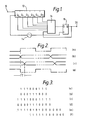
- a data input signal is applied via an input terminal 10 to a six stage shift register 12 which is clocked at say eight times the data rate by a clock signal generator 14.
- the outputs Q o to Q 5 of the shift register 12 are applied to respective inputs of a seven input majority logic circuit 16.
- An output of the circuit 16 is connected to a latching circuit 18 which is clocked in antiphase relative to the clocking of the shift register 12.
- An output of the latching circuit 18 is applied to an output terminal 20 and is also fed back to the seventh input of the circuit 16.
- the clock waveforms (a) and (d) of Figure 2 are applied to the clock inputs of the shift register 12 and the latching circuit 18, respectively, both of which are clocked on a low to high transition as indicated by the arrows applied to these transitions.
- the data signal, waveform (b) of Figure 2 is applied to the input terminal 10.
- the value of the input signal when sampled is stored serially in the shift register 12.
- the outputs Q O to Q 5 of the respective stages of the shift register 12 are applied to the majority logic circuit 16 together with the output the latch circuit 18.
- the circuit 16 has an odd number of inputs there will always be a majority decision output. Thus if three inputs are "l"s and the three others are "0"s then the output will be dependant on the output of the latch 18.
- the number of input signal errors which can be corrected is related to the number (n + 1) of the inputs to the majority logic circuit 16 and is defined generally as [(n)/2].
- n 6 then three error bits can be corrected, for example in Figure 3(a) the three "0"s will be corrected to all "l”s and conversely in Figure 3(b) the three "l”s will be corrected to all "0"s.
- Figures 3(c) and 3(d) illustrate that in order to correct three successive errors, that is the "0"s in Figure 3(c) and the "I"s in Figure 3(d), it is necessary to have four correct digits before and after the erroneous ones as opposed to three correct digits before and after the erroneous ones as shown in Figures 3(a) and 3(b).
- Figure 3(e) illustrates a signal having a distorted transition from 1 to 0 and Figure 3(f) illustrates how this signal can be estimated by the circuit in accordance with the present invention so that there is a single transition from "1" to "0".
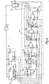
- Figure 4 is a schematic circuit diagram of an embodiment of the present invention having a feedback connection between the output of the latching circuit 18 and the majority logic circuit 16.
- the latching circuit 18 comprises part of an integrated circuit type CD 4013 and the shift register 12 comprises two six stage shift register integrated circuits 12A, 12B of type CD 4015, both of these integrated circuit types being manufactured by the Radio Corporation of America.
- the majority logic circuit 16 is constituted by a plurality of NAND-gates, EX-OR gates and inverters.
- circuit 16 may be regarded as comprising four identical modules 30, 40, 50 and 60 and several other components. Only one of the modules, the module 30, will be described in detail.
- Outputs Qo and Q 1 of the shift register circuit 12A are connected to the inputs of a NAND gate 22 and of an EX-OR gate 24.
- the output of the NAND gate 22 is inverted by an inverter 26 and is applied as one (31) of two inputs to the module 30, the other (32) of the two inputs being the output of the EX-OR gate 24.
- the input 31 is applied to an EX-OR gate 33 and to a NAND gate 34 and the other input 32 is applied to the EX-OR gate 33 and to an EX-OR gate 35.
- the output of the EX-OR gate 33 is applied as an input to a NAND gate 36.
- An output Q 2 of the shift register circuit 12A is connected as an input to the EX-OR gate 35 and the NAND gate 36, and, via an inverter 37, to the NAND gate 38.
- An output of the NAND gate 38 and an input of the EX-OR gate 35 comprise, respectively, inputs 41 and 42 of the module 40.
- a third input to the module 40 comprises the output Q 3 of the shift register circuit 12A.
- the outputs of the module 40 are applied as inputs 51 and 52 of the module 50. Additionally an output Qo' of the shift register circuit 12B is applied as a third input to the module 50. These three inputs are also applied to a NAND gate 72 whose output is connected to a second input of the NAND gate 78.
- the outputs of the module 50 comprise inputs 61 and 62 of the module 60 whose third input is the output Q 1 ' of the shift register circuit 12B. These three inputs are connected to a NAND gate 74 whose output comprises a third input of the NAND gate 78.
- the two outputs of the module 60 together with the feedback connection from the output of the latch 18 are applied to a NAND gate 76 whose output comprises a fourth input of the NAND gate 78.
- the output of the NAND gate 78 is connected to the data input D of the latch 18.
Landscapes
- Engineering & Computer Science (AREA)
- Computer Networks & Wireless Communication (AREA)
- Signal Processing (AREA)
- Quality & Reliability (AREA)
- Power Engineering (AREA)
- Logic Circuits (AREA)
- Detection And Prevention Of Errors In Transmission (AREA)
- Mobile Radio Communication Systems (AREA)
Applications Claiming Priority (2)
| Application Number | Priority Date | Filing Date | Title |
|---|---|---|---|
| GB08406627A GB2156117A (en) | 1984-03-14 | 1984-03-14 | Method of, and a circuit for, estimating true data from distorted digital data signals |
| GB8406627 | 1984-03-14 |
Publications (3)
| Publication Number | Publication Date |
|---|---|
| EP0155058A2 true EP0155058A2 (de) | 1985-09-18 |
| EP0155058A3 EP0155058A3 (en) | 1988-04-20 |
| EP0155058B1 EP0155058B1 (de) | 1991-08-28 |
Family
ID=10558065
Family Applications (1)
| Application Number | Title | Priority Date | Filing Date |
|---|---|---|---|
| EP19850200351 Expired EP0155058B1 (de) | 1984-03-14 | 1985-03-11 | Verfahren und Anordnung zur Abschätzung wahrer Daten in verzerrten Datensignalen |
Country Status (10)
| Country | Link |
|---|---|
| US (1) | US4686676A (de) |
| EP (1) | EP0155058B1 (de) |
| JP (1) | JPS60208133A (de) |
| AU (1) | AU579529B2 (de) |
| CA (1) | CA1241448A (de) |
| DE (1) | DE3583876D1 (de) |
| DK (1) | DK163776C (de) |
| GB (1) | GB2156117A (de) |
| HK (1) | HK78993A (de) |
| SG (1) | SG68793G (de) |
Cited By (5)
| Publication number | Priority date | Publication date | Assignee | Title |
|---|---|---|---|---|
| FR2653283A1 (fr) * | 1989-10-17 | 1991-04-19 | Lucas Ind Plc | Appareil destine a detecter des erreurs sur des trajets de communication. |
| EP0306757A3 (de) * | 1987-09-10 | 1991-07-24 | Nippon Motorola Ltd. | Schaltung für Fehlererkennung und Fehlerkorrektur |
| FR2669794A1 (fr) * | 1990-11-21 | 1992-05-29 | Motorola Inc | Systeme de detection d'erreur. |
| DE4238875A1 (de) * | 1992-11-19 | 1994-05-26 | Micrologica Computersysteme Gm | Aufzeichnungsgerät für Datenleitungen |
| GB2276517A (en) * | 1993-03-22 | 1994-09-28 | Nigel Howard Walton | Sampling and line noise reduction in parallel data transmission |
Families Citing this family (10)
| Publication number | Priority date | Publication date | Assignee | Title |
|---|---|---|---|---|
| US4764923A (en) * | 1987-03-03 | 1988-08-16 | Advance Micro Devices, Inc. | Digital receive filter circuit |
| JPH01166632A (ja) * | 1987-12-22 | 1989-06-30 | Mitsubishi Electric Corp | ディジタル信号の復号方法及びその回路 |
| US4989174A (en) * | 1988-10-27 | 1991-01-29 | Commodore Business Machines, Inc. | Fast gate and adder for microprocessor ALU |
| GB2246687B (en) * | 1990-04-06 | 1994-04-27 | Plessey Co Ltd | Improvements relating to data transmission systems |
| US5023892A (en) * | 1990-04-06 | 1991-06-11 | Printer Systems Corporation | System for detecting and correcting signal distortion |
| US5719904A (en) * | 1994-10-13 | 1998-02-17 | Samsung Electronics Co., Ltd. | Data restoring circuit |
| US5761240A (en) * | 1996-02-06 | 1998-06-02 | Ericsson Inc. | Method and apparatus for determining an optical communications channel without loss of channel messages on a current communications channel |
| US5948116A (en) * | 1996-02-23 | 1999-09-07 | Texas Instruments Deutschland, Gmbh | Bit error correction algorithm |
| JP3930513B2 (ja) * | 2003-05-21 | 2007-06-13 | 富士通株式会社 | 多数決論理回路を有するフリップフロップ回路 |
| US9710012B2 (en) * | 2012-11-21 | 2017-07-18 | Sandisk Technologies Llc | Timing optimized implementation of algorithm to reduce switching rate on high throughput wide buses |
Family Cites Families (16)
| Publication number | Priority date | Publication date | Assignee | Title |
|---|---|---|---|---|
| GB152702A (en) * | 1919-04-23 | 1920-10-25 | Thomas Lenaghan | An improved automatic telephone system |
| FR1396666A (fr) * | 1963-04-30 | 1965-04-23 | Rca Corp | Montage pour la détection et la correction des distorisons dans un signal d'information |
| FR1404512A (fr) * | 1964-05-08 | 1965-07-02 | Cit Alcatel | Récepteurs de télégraphie |
| DE1252727B (de) * | 1965-03-01 | 1967-10-26 | International Business Machines Corporation, Armonk, NY (V St A) | Verfahren zum störungsfreien Empfang übertragener Daten |
| GB1258595A (de) * | 1969-06-23 | 1971-12-30 | ||
| GB1253309A (en) * | 1969-11-21 | 1971-11-10 | Marconi Co Ltd | Improvements in or relating to data processing arrangements |
| US3859655A (en) * | 1970-10-01 | 1975-01-07 | Nederlanden Staat | System for the transfer of two states by multiple scanning |
| SU585549A1 (ru) * | 1976-04-06 | 1977-12-25 | Предприятие П/Я А-7160 | Резервированное запоминающее устройство |
| DE2740840A1 (de) * | 1977-08-09 | 1979-02-22 | Bbc Brown Boveri & Cie | Anlage zur ueberwachung der aussagekraft von auf einer anzahl n funktionell parallelgeschalteter datenkanaelen aufgebrachter elektrischer daten sowie deren verwendung |
| SU656218A1 (ru) * | 1977-12-26 | 1979-04-05 | Ленинградский Ордена Ленина Электротехнический Институт Им. В.И.Ульянова (Ленина) | Счетчик с коррекцией ошибок |
| US4241311A (en) * | 1979-02-01 | 1980-12-23 | Telex Computer Products, Inc. | Digital majority noise filter for bi-level data reception |
| DE3036614A1 (de) * | 1980-09-29 | 1982-05-13 | Siemens AG, 1000 Berlin und 8000 München | Verfahren zur erkennung von digitalinformation bei einer digitalen informationsuebertragung, insbesondere informationsuebertragung in mobilfunk-kommunikationssystemen |
| DE3036612A1 (de) * | 1980-09-29 | 1982-05-13 | Siemens AG, 1000 Berlin und 8000 München | Verfahren zur erkennung von digitalinformation bei einer digitalen informationsuebertragung, insbesondere informationsuebertragung in mobilfunk-kommunikationssystemen |
| US4375683A (en) * | 1980-11-12 | 1983-03-01 | August Systems | Fault tolerant computational system and voter circuit |
| US4484330A (en) * | 1982-03-08 | 1984-11-20 | At&T Bell Laboratories | Majority vote circuit |
| NL8202364A (nl) * | 1982-06-11 | 1984-01-02 | Philips Nv | Serie-parallel-serie schuifregistergeheugen, waarbij het parallelopslagregister mede redundante enkelvoudige opslagregisters bevat, en afbeeldtoestel, voorzien van een zodanig georganiseerd beeldgeheugen. |
-
1984
- 1984-03-14 GB GB08406627A patent/GB2156117A/en not_active Withdrawn
-
1985
- 1985-03-07 CA CA000475996A patent/CA1241448A/en not_active Expired
- 1985-03-11 DK DK110685A patent/DK163776C/da active
- 1985-03-11 AU AU39712/85A patent/AU579529B2/en not_active Ceased
- 1985-03-11 EP EP19850200351 patent/EP0155058B1/de not_active Expired
- 1985-03-11 DE DE8585200351T patent/DE3583876D1/de not_active Expired - Lifetime
- 1985-03-13 JP JP60048437A patent/JPS60208133A/ja active Granted
- 1985-03-14 US US06/711,783 patent/US4686676A/en not_active Expired - Lifetime
-
1993
- 1993-05-26 SG SG687/93A patent/SG68793G/en unknown
- 1993-08-05 HK HK789/93A patent/HK78993A/en not_active IP Right Cessation
Cited By (5)
| Publication number | Priority date | Publication date | Assignee | Title |
|---|---|---|---|---|
| EP0306757A3 (de) * | 1987-09-10 | 1991-07-24 | Nippon Motorola Ltd. | Schaltung für Fehlererkennung und Fehlerkorrektur |
| FR2653283A1 (fr) * | 1989-10-17 | 1991-04-19 | Lucas Ind Plc | Appareil destine a detecter des erreurs sur des trajets de communication. |
| FR2669794A1 (fr) * | 1990-11-21 | 1992-05-29 | Motorola Inc | Systeme de detection d'erreur. |
| DE4238875A1 (de) * | 1992-11-19 | 1994-05-26 | Micrologica Computersysteme Gm | Aufzeichnungsgerät für Datenleitungen |
| GB2276517A (en) * | 1993-03-22 | 1994-09-28 | Nigel Howard Walton | Sampling and line noise reduction in parallel data transmission |
Also Published As
| Publication number | Publication date |
|---|---|
| DK110685D0 (da) | 1985-03-11 |
| DK163776C (da) | 1992-09-07 |
| DK163776B (da) | 1992-03-30 |
| AU3971285A (en) | 1985-09-19 |
| AU579529B2 (en) | 1988-11-24 |
| HK78993A (en) | 1993-08-13 |
| JPS60208133A (ja) | 1985-10-19 |
| SG68793G (en) | 1993-08-06 |
| US4686676A (en) | 1987-08-11 |
| EP0155058A3 (en) | 1988-04-20 |
| DE3583876D1 (de) | 1991-10-02 |
| JPH0453338B2 (de) | 1992-08-26 |
| EP0155058B1 (de) | 1991-08-28 |
| GB2156117A (en) | 1985-10-02 |
| CA1241448A (en) | 1988-08-30 |
| DK110685A (da) | 1985-09-15 |
Similar Documents
| Publication | Publication Date | Title |
|---|---|---|
| US5412698A (en) | Adaptive data separator | |
| US4686676A (en) | Apparatus and method for determining true data in a digital data stream from distorted data | |
| EP0150072B1 (de) | Dekodierschaltung | |
| US4965884A (en) | Data alignment method and apparatus | |
| US5577078A (en) | Edge detector | |
| JPH08149120A (ja) | 非同期シリアルデータ受信装置 | |
| JP3433426B2 (ja) | マンチェスタ符号化データをデコーディングするための方法および装置 | |
| JPH03191633A (ja) | データ転送方式 | |
| US5132993A (en) | Shift register circuit | |
| US5878096A (en) | Digital filter having phase-adjustment ability | |
| US4714892A (en) | Differential phase shift keying demodulator | |
| EP1804449A2 (de) | Dekodierschaltung für ein zweiphasiges BPSK-Signal | |
| CA2037219C (en) | Electronic circuit for generating error detection codes for digital signals | |
| US4539680A (en) | Chip to chip information bit transmission process and device | |
| US5901189A (en) | Symmetrical correlator | |
| US5361289A (en) | Synchronous counter circuit having a plurality of cascade-connected counters | |
| US5930275A (en) | Clock error detection circuit | |
| US20010017905A1 (en) | Data receiving system robust against jitter of clock | |
| EP0282924B1 (de) | Kodierschaltung mit bipolarer Acht- und Sechsnullfolgensubstitution | |
| US6603336B1 (en) | Signal duration representation by conformational clock cycles in different time domains | |
| JP3478290B2 (ja) | Duty補正回路 | |
| EP0983660A1 (de) | Schaltung und verfahren zum empfang von daten | |
| JP3001414B2 (ja) | 符号誤り訂正装置 | |
| JP3458782B2 (ja) | Duty補正回路 | |
| KR920004806Y1 (ko) | 직렬통신 잡음 제거회로 |
Legal Events
| Date | Code | Title | Description |
|---|---|---|---|
| PUAI | Public reference made under article 153(3) epc to a published international application that has entered the european phase |
Free format text: ORIGINAL CODE: 0009012 |
|
| AK | Designated contracting states |
Designated state(s): DE FR GB IT SE |
|
| PUAL | Search report despatched |
Free format text: ORIGINAL CODE: 0009013 |
|
| AK | Designated contracting states |
Kind code of ref document: A3 Designated state(s): DE FR GB IT SE |
|
| RAP3 | Party data changed (applicant data changed or rights of an application transferred) |
Owner name: N.V. PHILIPS' GLOEILAMPENFABRIEKEN Owner name: PHILIPS ELECTRONIC AND ASSOCIATED INDUSTRIES LIMIT |
|
| 17P | Request for examination filed |
Effective date: 19880930 |
|
| 17Q | First examination report despatched |
Effective date: 19900703 |
|
| GRAA | (expected) grant |
Free format text: ORIGINAL CODE: 0009210 |
|
| AK | Designated contracting states |
Kind code of ref document: B1 Designated state(s): DE FR GB IT SE |
|
| REF | Corresponds to: |
Ref document number: 3583876 Country of ref document: DE Date of ref document: 19911002 |
|
| ITF | It: translation for a ep patent filed | ||
| ET | Fr: translation filed | ||
| RAP4 | Party data changed (patent owner data changed or rights of a patent transferred) |
Owner name: N.V. PHILIPS' GLOEILAMPENFABRIEKEN Owner name: PHILIPS ELECTRONICS UK LIMITED |
|
| PLBE | No opposition filed within time limit |
Free format text: ORIGINAL CODE: 0009261 |
|
| STAA | Information on the status of an ep patent application or granted ep patent |
Free format text: STATUS: NO OPPOSITION FILED WITHIN TIME LIMIT |
|
| 26N | No opposition filed | ||
| EAL | Se: european patent in force in sweden |
Ref document number: 85200351.6 |
|
| ITPR | It: changes in ownership of a european patent |
Owner name: CAMBIO RAGIONE SOCIALE;PHILIPS ELECTRONICS N.V. |
|
| REG | Reference to a national code |
Ref country code: FR Ref legal event code: CD |
|
| PGFP | Annual fee paid to national office [announced via postgrant information from national office to epo] |
Ref country code: SE Payment date: 19970324 Year of fee payment: 13 |
|
| PG25 | Lapsed in a contracting state [announced via postgrant information from national office to epo] |
Ref country code: SE Free format text: LAPSE BECAUSE OF NON-PAYMENT OF DUE FEES Effective date: 19980312 |
|
| REG | Reference to a national code |
Ref country code: FR Ref legal event code: CD |
|
| EUG | Se: european patent has lapsed |
Ref document number: 85200351.6 |
|
| PGFP | Annual fee paid to national office [announced via postgrant information from national office to epo] |
Ref country code: FR Payment date: 20010326 Year of fee payment: 17 |
|
| PGFP | Annual fee paid to national office [announced via postgrant information from national office to epo] |
Ref country code: GB Payment date: 20010330 Year of fee payment: 17 |
|
| PGFP | Annual fee paid to national office [announced via postgrant information from national office to epo] |
Ref country code: DE Payment date: 20010516 Year of fee payment: 17 |
|
| REG | Reference to a national code |
Ref country code: GB Ref legal event code: IF02 |
|
| PG25 | Lapsed in a contracting state [announced via postgrant information from national office to epo] |
Ref country code: GB Free format text: LAPSE BECAUSE OF NON-PAYMENT OF DUE FEES Effective date: 20020311 |
|
| PG25 | Lapsed in a contracting state [announced via postgrant information from national office to epo] |
Ref country code: DE Free format text: LAPSE BECAUSE OF NON-PAYMENT OF DUE FEES Effective date: 20021001 |
|
| GBPC | Gb: european patent ceased through non-payment of renewal fee |
Effective date: 20020311 |
|
| PG25 | Lapsed in a contracting state [announced via postgrant information from national office to epo] |
Ref country code: FR Free format text: LAPSE BECAUSE OF NON-PAYMENT OF DUE FEES Effective date: 20021129 |
|
| REG | Reference to a national code |
Ref country code: FR Ref legal event code: ST |