EP0144568A2 - Multiplikationswerk und Verfahren zu dessen Betrieb - Google Patents
Multiplikationswerk und Verfahren zu dessen Betrieb Download PDFInfo
- Publication number
- EP0144568A2 EP0144568A2 EP84110830A EP84110830A EP0144568A2 EP 0144568 A2 EP0144568 A2 EP 0144568A2 EP 84110830 A EP84110830 A EP 84110830A EP 84110830 A EP84110830 A EP 84110830A EP 0144568 A2 EP0144568 A2 EP 0144568A2
- Authority
- EP
- European Patent Office
- Prior art keywords
- bits
- accumulator
- unit
- inputs
- arithmetic
- Prior art date
- Legal status (The legal status is an assumption and is not a legal conclusion. Google has not performed a legal analysis and makes no representation as to the accuracy of the status listed.)
- Granted
Links
- 238000000034 method Methods 0.000 title claims description 5
- 230000000295 complement effect Effects 0.000 description 3
- 238000011161 development Methods 0.000 description 1
- 230000018109 developmental process Effects 0.000 description 1
- 230000000694 effects Effects 0.000 description 1
Images
Classifications
-
- G—PHYSICS
- G06—COMPUTING; CALCULATING OR COUNTING
- G06F—ELECTRIC DIGITAL DATA PROCESSING
- G06F7/00—Methods or arrangements for processing data by operating upon the order or content of the data handled
- G06F7/38—Methods or arrangements for performing computations using exclusively denominational number representation, e.g. using binary, ternary, decimal representation
- G06F7/48—Methods or arrangements for performing computations using exclusively denominational number representation, e.g. using binary, ternary, decimal representation using non-contact-making devices, e.g. tube, solid state device; using unspecified devices
- G06F7/52—Multiplying; Dividing
- G06F7/523—Multiplying only
- G06F7/533—Reduction of the number of iteration steps or stages, e.g. using the Booth algorithm, log-sum, odd-even
- G06F7/5334—Reduction of the number of iteration steps or stages, e.g. using the Booth algorithm, log-sum, odd-even by using multiple bit scanning, i.e. by decoding groups of successive multiplier bits in order to select an appropriate precalculated multiple of the multiplicand as a partial product
- G06F7/5336—Reduction of the number of iteration steps or stages, e.g. using the Booth algorithm, log-sum, odd-even by using multiple bit scanning, i.e. by decoding groups of successive multiplier bits in order to select an appropriate precalculated multiple of the multiplicand as a partial product overlapped, i.e. with successive bitgroups sharing one or more bits being recoded into signed digit representation, e.g. using the Modified Booth Algorithm
- G06F7/5338—Reduction of the number of iteration steps or stages, e.g. using the Booth algorithm, log-sum, odd-even by using multiple bit scanning, i.e. by decoding groups of successive multiplier bits in order to select an appropriate precalculated multiple of the multiplicand as a partial product overlapped, i.e. with successive bitgroups sharing one or more bits being recoded into signed digit representation, e.g. using the Modified Booth Algorithm each bitgroup having two new bits, e.g. 2nd order MBA
Definitions
- the invention relates to a multiplication unit according to the preamble of claim 1 and to a method for its operation.
- the object of the invention is to provide a multiplication unit of this type with which a high operating speed can be achieved and which only requires an n-digit arithmetic unit and an n-digit accumulator for multiplying n-digit binary numbers represented in two's complement. According to the invention this is achieved by designing the multiplication unit according to the characterizing part of patent claim 1.
- the advantage that can be achieved with the invention is, in particular, that only an n-digit multiple sliding mechanism is required to shift the linking results output by the arithmetic unit to the accumulator.
- Claims 2 to 5 relate to advantageous refinements and developments of the multiplication unit according to the invention, while claim 6 is directed to a preferred method for operating the multiplication unit according to the invention.
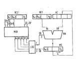
- An n-digit register RE1 is provided, which represents the binary number X as an n-digit binary number with bits x n-1 , x n-2 ... x 0 in two's complement multiplicands.
- x n-1 is the most significant bit, which indicates a negative sign with a value "1" and a positive sign of the binary number with a value "0".
- x 0 represents the least significant bit.
- the output of RE1 is connected to operand input A of an arithmetic logic unit RW, the second operand input B of which is connected to the output of an n-digit accumulator AC.
- the output of RW is connected to the input of a multiple sliding mechanism MS, the output of which is connected to the input of the accumulator AC.
- a register RE2 is used to hold the multiplier Y, also represented as a binary number in two's complement.
- yn-1 means the sign bit, y 0 the bit with the lowest value.
- a multiplexer MUX with n + 3 inputs EO ', EO, E1 ... E (n + 1) selects five immediately adjacent bits, for example y 1 ... y 5 , and switches them to its outputs AO to A4 by. From the bits that can be tapped at AO to A4, an operation command OB is derived via a logic circuit element LSG, which occurs at a first output 1 of LSG and is supplied to the operation command input 2 of the arithmetic logic unit RW.
- the operation command OB causes the arithmetic unit to either subtract the binary number present at operand input A from the binary number present at operand input B, to add the number present at A to the number present at B or to add the binary number present at B to the output of RW to switch through.
- a shift command SB is derived from the bits present at AO to A4 via LSG, which occurs at an output 3 of LSG and is fed to a control input of the multiple shift mechanism MS.
- the shift command SB effects a so-called arithmetic shift of the binary number contained in the n-digit multiple shift mechanism MS by a certain number of digits, ie one or more digits, each to the right, as indicated by arrow 4.
- bits of the binary number contained in MS are denoted by s n-1 , s n-2 .... S 0 , where s n-1 indicates the sign of this number as the most significant bit and s 0 means the bit with the lowest value, if an arithmetic shift of this number by three places to the right, bits s 0 , s 1 and s 2 are dropped, while the three vacant positions at the left end of MS are now each assigned the sign bit sn-1. After this shift, the binary number s n-1 , s n-1 ' s n-1 , s n-1 , s n-2 ... s 3 is in MS.
- s 0 is produced in RW and is fed to the multiple sliding mechanism MS.
- the shift command SB derived via LSG causes MS to arithmetically shift this first link result to the right by a certain number of digits in the manner already described.
- the number now contained in MS which has bits s n-1 , s n-1 , s n-1 , s n-1 , s n-2 .... s 3 , for example, when shifted by three digits then fed to the accumulator AC as the first subtotal.
- the multiplexer MUX switches through the bits y 1 ... y 5 at the inputs offset two positions to the left, ie at E1 ... E5, to AO to A4.
- two new commands, OB and SB are derived, from which OB causes the arithmetic logic unit RW to link the number X present at A with the first subtotal supplied by AC after one of the three possible operations, so that a second Link result is created.
- this is arithmetically shifted to the right by a certain number of digits, a second subtotal being generated in MS in the manner described, which is supplied to AC.
- MUX switches through the bits at the last five inputs E (n-3), E (n-2), E (n-1), En and E (n + 1), the last three inputs each are assigned the same bit as the drawing now shows g. Therefore, the bits y n-3 ... y n-1 , y n-1 , y n-1 can be picked up at the outputs AO ... A4.
- the OB and SB commands derived from this cause in RW. a combination of X with the subtotal located in AC and an arithmetic shift of the combination result in MS according to SB.
- the binary number created in MS then represents the product of the binary numbers X and Y, which consists of the n most significant bits. If n is odd number, then in the last step E (n + 1) is no longer scanned, so that the bits y n-4 ... y n-1 , y n-1 are switched through.
- the OB and SB commands are formed from the bits of the number Y that can be tapped from AO ... A4 according to the following table, in which the first five columns are assigned to the outputs AO ... A4 in the first line, while the sixth and the seventh column each contain the commands OB and SB.
- the bits that occur simultaneously at the inputs and outputs of LSB are each on one line.
- OB 1 means that the operands at A and B are added.
- the numerical values in the column for SB immediately indicate the number of digits by which the link result output from RW to MS is to be shifted arithmetically to the right in MS.
- the multiple sliding mechanism MS is, for example, constructed in the manner of the devices referred to as "barrel shifters", which are described in the book “Introduction to VLSI Systems” by C.Mead and L.Conway, Addison-Wesley Publishing Comp., Reading, Mass ., Oct. 1980, on pages 157 to 161.
- the logic circuit element LSG can consist, for example, of a read-only memory or a logic gate circuit.
Abstract
Description
- Die Erfindung bezieht sich auf ein Multiplikationswerk nach dem Oberbegriff des Patentanspruchs 1 und auf ein Verfahren zu dessen Betrieb.
- Aufgabe der Erfindung ist es, ein Multiplikationswerk dieser Art anzugeben, mit dem eine hohe Arbeitsgeschwindigkeit erreichbar ist und das zur Multiplikation von im Zweierkomplement dargestellten n-stelligen binären Zahlen lediglich ein n-stelliges Rechenwerk und einen n-stelligen Akkumulator benötigt. Erfindungsgemäß wird das durch eine Ausbildung des Multiplikationswerks nach dem kennzeichnenden Teil des Patentanspruchs 1 erreicht.
- Der mit der Erfindung erzielbare Vorteil besteht insbesondere darin, daß nur ein n-stelliges Mehrfach-Schiebewerk zur Verschiebung der vom Rechenwerk an den Akkumulator ausgegebenen Verknüpfungsergebnisse erforderlich ist.
- Die Ansprüche 2 bis 5 betreffen vorteilhafte Ausgestaltungen und Weiterbildungen des Multiplikationswerks nach der Erfindung, während der Anspruch 6 auf ein bevorzugtes Verfahren zum Betrieb des erfindungsgemäßen Multiplikationswerks gerichtet ist.
- Die Erfindung wird nachfolgend anhand der Zeichnung näher erläutert. Dabei ist ein n-stelliges Register RE1 vorgesehen, das den als eine n-stellige binäre Zahl X mit den Bits xn-1, xn-2 ...x0 im Zweierkomplement dargestellten Multiplikanden enthält. xn-1 ist dabei das höchstwertige Bit, das durch einen Wert "1" ein negatives Vorzeichen und durch einen Wert "0" ein positives Vorzeichen der binären Zahl angibt. x0 stellt das Bit niedrigster Wertigkeit dar. Der Ausgang von RE1 ist mit dem Operandeneingang A eines Rechenwerks RW verbunden, dessen zweiter Operandeneingang B mit dem Ausgang eines n-stelligen Akkumulators AC beschaltet ist. Der Ausgang von RW ist mit dem Eingang eines Mehrfach-Schiebewerks MS verbunden, dessen Ausgang mit dem Eingang des Akkumulators AC beschaltet ist.
- Ein Register RE2 dient zur Aufnahme des ebenfalls als binäre Zahl im Zweierkomplement dargestellten Multiplikators Y. Auch hier bedeutet yn-1 das Vorzeichenbit, y0 das Bit niedrigster Wertigkeit. Ein Multiplexer MUX mit n+3 Eingängen EO', EO, E1 ... E(n+1) wählt jeweils fünf einander unmittelbar benachbarte Bits, z.B. y1 ... y5, aus und schaltet sie an seine Ausgänge AO bis A4 durch. Aus den an AO bis A4 jeweils abgreifbaren Bits wird über ein logisches Schaltungsglied LSG ein Operationsbefehl OB abgeleitet, der an einem ersten Ausgang 1 von LSG auftritt und dem Operationsbefehlseingang 2 des Rechenwerks RW zugeführt wird. Der Operationsbefehl OB veranlaßt das Rechenwerk, die am Operandeneingang A anliegende binäre Zahl entweder von der am Operandeneingang B anliegenden binären Zahl zu subtrahieren, die bei A anliegende Zahl zu der bei B anliegenden zu addieren oder die bei B anliegende binäre Zahl an den Ausgang von RW durchzuschalten. Weiterhin wird aus den an AO bis A4 anliegenden Bits über LSG ein Verschiebebefehl SB abgeleitet, der an einem Ausgang 3 von LSG auftritt und einem Steuereingang des Mehrfach-Schiebewerks MS zugeführt wird. Der Verschiebebefehl SB bewirkt eine sog. arithmetische Verschiebung der im n-stelligen Mehrfach-Schiebewerk MS enthaltenen binären Zahl, um eine bestimmte Stellenanzahl, d.h. um eine oder um mehrere Stellen, jeweils nach rechts, wie durch den Pfeil 4 angedeutet ist. Werden die Bits der in MS enthaltenen binären Zahl mit sn-1, sn-2.... S0 bezeichnet, wobei sn-1 als das höchstwertige Bit das Vorzeichen dieser Zahl angibt und s0 das Bit niedrigster Wertigkeit bedeutet, so werden bei einer arithmetischen Verschiebung dieser Zahl um drei Stellen nach rechts die Bits s0, s1 und s2 fallengelassen, während die drei frei werdenden Stellen am linken Ende von MS nunmehr jeweils mit dem Vorzeichenbit sn-1 belegt werden. Damit steht nach dieser Verschiebung die binäre Zahl sn-1, sn-1' sn-1, sn-1 , sn-2 ... s3 in MS.
- Zur Multiplikation von X und Y wird nun so verfahren, daß in sämtliche Stellen des Akkumulators AC und des Mehrfach-Schiebewerks MS zunächst jeweils "0"-Bits eingegeben werden. Im Multiplexer MUX werden die an seinen Eingängen EO', EO ...E3 liegenden Bits an seine Ausgänge AO ... A4 durchgeschaltet, wobei am Eingang EO' ständig eine "0" anliegt. Hieraus werden in LSG Befehle OB und SB abgeleitet, wobei OB eine der drei genannten Operationen des Rechenwerks RW veranlaßt, die auf die am Operandeneingang A liegende Zahl X und auf die aus dem Akkumulator AC dem Operandeneingang B zugeführten "0"-Bits angewendet wird. In RW entsteht ein erstes Verknüpfungsergebnis sn-1 ...s0, das dem Mehrfach-Schiebewerk MS zugeführt wird. Der über LSG abgeleitete Verschiebebefehl SB veranlaßt MS, dieses erste Verknüpfungsergebnis in der bereits beschriebenen Weise um eine bestimmte Stellenzahl nach rechts arithmetisch zu verschieben. Die nunmehr in MS enthaltene Zahl, die z.B. bei einer Verschiebung um drei Stellen die Bits sn-1, sn-1, sn-1, sn-1, sn-2....s3 aufweist, wird dann dem Akkumulator AC als erste Zwischensumme zugeführt.
- Anschließend werden vom Multiplexer MUX die an den um zwei Stellen nach links versetzten Eingängen, d.h. an E1 ...E5, anliegenden Bits y1 ...y5 auf AO bis A4 durchgeschaltet. Über LSG werden zwei neue Befehle,OB und SB abgeleitet, von denen OB das Rechenwerk RW veranlaßt, die bei A anliegende Zahl X mit der bei B anliegenden, von AC zugeführten ersten Zwischensumme nach einer der drei möglichen Operationen zu verknüpfen, so daß ein zweites Verknüpfungsergebnis entsteht. Dieses wird gemäß SB um eine bestimmte Stellenzahl arithmetisch nach rechts verschoben, wobei in MS in der beschriebenen Weise eine zweite Zwischensumme entsteht, die AC zugeführt wird.
- Es folgen weitere gleichartige Verfahrensschritte, wobei der Multiplexer MUX bei jedem neuen Schritt die jeweils um zwei Stellen nach links versetzten Bits des Multiplikators Y an seine Ausgänge durchschaltet.
- Bei letzten Schritt werden von MUX die Bits an den letzten fünf Eingängen E(n-3), E(n-2), E(n-1), En und E(n+1) durchgeschaltet, wobei die letzten drei Eingänge jeweils mit demselben Bit belegt sind, wie die Zeich- nung zeigt. Daher sind die Bits yn-3 ...yn-1, yn-1, yn-1 an den Ausgähgen AO ...A4 abgreifbar. Die hieraus abgeleiteten Befehle OB und SB veranlassen in RW. eine Verknüpfung von X mit der sich in AC befindenden Zwischensumme und eine arithmetische Verschiebung des Verknüpfungsergebnisses in MS gemäß SB. Die hierbei in MS entstandene binäre Zahl stellt dann das Produkt der Binärzahlen X und Y dar, das aus den n am meisten signifikanten Bits besteht. Ist n ungeradzahlinq, so wird beim letzten Schritt E(n+1) nicht mehr abgetastet, so daß die Bits yn-4... yn-1, yn-1durchgeschaltet werden.
- Die Bildung der Befehle OB und SB aus den jeweils bei AO ...A4 abgreifbaren Bits der Zahl Y erfolgt nach folgender Tabelle, bei der die ersten fünf Spalten den in der ersten Zeile stehenden Ausgängen AO ... A4 zugeordnet sind, während die sechste und siebente Spalte jeweils die Befehle OB und SB enthalten. Die an den Eingängen und Ausgängen von LSB gleichzeitig auftretenden Bits stehen dabei jeweils in einer Zeile.

- Dabei bedeutet OB = 1, daß die Operanden an A und B addiert werden. OB = -1 bedeutet, daß der Operand an A von dem Operanden an B subtrahiert wird, während OB = 0 aussagt, daß der Operand an B direkt auf den Ausgang von RW durchgeschaltet werden soll. Die Zahlenwerte in der Spalte für SB geben jeweils unmittelbar die Anzahl der Stellen an, um die das von RW an MS ausgegebene Verknüpfungsergebnis in MS arithmetisch nach rechts verschoben werden soll.
- Das Mehrfach-Schiebewerk MS ist beispielsweise so aufgebaut, wie die als "Barrel Shifter" bezeichneten Einrichtungen, die in dem Buch "Introduction to VLSI-Systems" von C.Mead und L.Conway, Addison-Wesley Publishing Comp., Reading, Mass., Okt. 1980, auf den Seiten 157 bis 161 beschrieben sind. Das logische Schaltungsglied LSG kann beispielsweise aus einem Festwertspeicher oder einer logischen Gatterschaltung bestehen.
Claims (6)
Applications Claiming Priority (2)
| Application Number | Priority Date | Filing Date | Title |
|---|---|---|---|
| DE19833335424 DE3335424A1 (de) | 1983-09-29 | 1983-09-29 | Multiplikationswerk und verfahren zu dessen betrieb |
| DE3335424 | 1983-09-29 |
Publications (3)
| Publication Number | Publication Date |
|---|---|
| EP0144568A2 true EP0144568A2 (de) | 1985-06-19 |
| EP0144568A3 EP0144568A3 (en) | 1988-01-27 |
| EP0144568B1 EP0144568B1 (de) | 1992-06-17 |
Family
ID=6210497
Family Applications (1)
| Application Number | Title | Priority Date | Filing Date |
|---|---|---|---|
| EP84110830A Expired - Lifetime EP0144568B1 (de) | 1983-09-29 | 1984-09-11 | Multiplikationswerk und Verfahren zu dessen Betrieb |
Country Status (4)
| Country | Link |
|---|---|
| US (1) | US4679165A (de) |
| EP (1) | EP0144568B1 (de) |
| JP (1) | JPS6093550A (de) |
| DE (2) | DE3335424A1 (de) |
Cited By (1)
| Publication number | Priority date | Publication date | Assignee | Title |
|---|---|---|---|---|
| EP0825523A1 (de) * | 1996-08-09 | 1998-02-25 | Siemens Aktiengesellschaft | Verfahren und Schaltung zur Multiplikation eines Multiplikanden und eines Multiplikators nach dem Booth-Verfahren in iterativen Schritten |
Families Citing this family (5)
| Publication number | Priority date | Publication date | Assignee | Title |
|---|---|---|---|---|
| US4972362A (en) * | 1988-06-17 | 1990-11-20 | Bipolar Integrated Technology, Inc. | Method and apparatus for implementing binary multiplication using booth type multiplication |
| US4970676A (en) * | 1989-04-04 | 1990-11-13 | Rca Licensing Corporation | Digital word-serial multiplier circuitry |
| DE19637369C2 (de) * | 1996-09-13 | 2001-11-15 | Micronas Gmbh | Digitaler Signalprozessor mit Multipliziereinrichtung und -Verfahren |
| US5958000A (en) * | 1996-11-15 | 1999-09-28 | Samsung Electronics, Co. Ltd. | Two-bit booth multiplier with reduced data path width |
| US6991003B2 (en) * | 2003-07-28 | 2006-01-31 | M.Braun, Inc. | System and method for automatically purifying solvents |
Citations (3)
| Publication number | Priority date | Publication date | Assignee | Title |
|---|---|---|---|---|
| US3192363A (en) * | 1961-05-24 | 1965-06-29 | Ibm | Binary multipler for skipping a string of zeroes or ones |
| US4122527A (en) * | 1975-11-04 | 1978-10-24 | Motorola, Inc. | Emitter coupled multiplier array |
| US4334284A (en) * | 1979-12-31 | 1982-06-08 | Sperry Corporation | Multiplier decoding using parallel MQ register |
Family Cites Families (13)
| Publication number | Priority date | Publication date | Assignee | Title |
|---|---|---|---|---|
| JPS52117893A (en) * | 1976-03-31 | 1977-10-03 | Hiyuuga Seirenshiyo Kk | Water slag apparatus for feronickel slag |
| US4130879A (en) * | 1977-07-15 | 1978-12-19 | Honeywell Information Systems Inc. | Apparatus for performing floating point arithmetic operations using submultiple storage |
| US4238833A (en) * | 1979-03-28 | 1980-12-09 | Monolithic Memories, Inc. | High-speed digital bus-organized multiplier/divider system |
| JPS57141753A (en) * | 1981-02-25 | 1982-09-02 | Nec Corp | Multiplication circuit |
| DE3134057A1 (de) * | 1981-08-28 | 1983-03-31 | Siemens AG, 1000 Berlin und 8000 München | Datenverarbeitungsanlage |
| JPS6177648A (ja) * | 1984-09-26 | 1986-04-21 | 新日本製鐵株式会社 | 水スラリ−状粒状物の乾燥方法 |
| JPS61163146A (ja) * | 1985-01-07 | 1986-07-23 | 株式会社 片山化学工業研究所 | 粒状スラグの脱水促進処理方法及び処理剤 |
| JPH0312347A (ja) * | 1989-06-12 | 1991-01-21 | Sumitomo Metal Ind Ltd | セメント瓦用水砕スラグの製造方法 |
| JPH03218952A (ja) * | 1990-01-23 | 1991-09-26 | Nippon Steel Chem Co Ltd | 水砕スラグ粉の製造方法 |
| JPH06183795A (ja) * | 1992-12-17 | 1994-07-05 | Daido Gakuen | フェロニッケルスラグセメント |
| JP2007146223A (ja) * | 2005-11-28 | 2007-06-14 | Hyuga Seirensho:Kk | ロータリーキルンダストの処理方法 |
| JP4777829B2 (ja) * | 2006-06-02 | 2011-09-21 | 日本冶金工業株式会社 | 骨材 |
| JP2008025934A (ja) * | 2006-07-24 | 2008-02-07 | Jfe Steel Kk | 脱珪スラグ粗精鉱の製造方法 |
-
1983
- 1983-09-29 DE DE19833335424 patent/DE3335424A1/de not_active Withdrawn
-
1984
- 1984-07-06 US US06/628,585 patent/US4679165A/en not_active Expired - Fee Related
- 1984-09-11 DE DE8484110830T patent/DE3485774D1/de not_active Expired - Fee Related
- 1984-09-11 EP EP84110830A patent/EP0144568B1/de not_active Expired - Lifetime
- 1984-09-26 JP JP59201402A patent/JPS6093550A/ja active Pending
Patent Citations (3)
| Publication number | Priority date | Publication date | Assignee | Title |
|---|---|---|---|---|
| US3192363A (en) * | 1961-05-24 | 1965-06-29 | Ibm | Binary multipler for skipping a string of zeroes or ones |
| US4122527A (en) * | 1975-11-04 | 1978-10-24 | Motorola, Inc. | Emitter coupled multiplier array |
| US4334284A (en) * | 1979-12-31 | 1982-06-08 | Sperry Corporation | Multiplier decoding using parallel MQ register |
Non-Patent Citations (1)
| Title |
|---|
| ELECTRONICS LETTERS, Band 16, Nr. 2, 17. Januar 1980, Seiten 53-54; E. AMBIKAIRAJAH et al.: "Technique for performing multiplication on a 16-bit microprocessor using an extension of booth's algorithm" * |
Cited By (1)
| Publication number | Priority date | Publication date | Assignee | Title |
|---|---|---|---|---|
| EP0825523A1 (de) * | 1996-08-09 | 1998-02-25 | Siemens Aktiengesellschaft | Verfahren und Schaltung zur Multiplikation eines Multiplikanden und eines Multiplikators nach dem Booth-Verfahren in iterativen Schritten |
Also Published As
| Publication number | Publication date |
|---|---|
| EP0144568A3 (en) | 1988-01-27 |
| DE3485774D1 (de) | 1992-07-23 |
| EP0144568B1 (de) | 1992-06-17 |
| US4679165A (en) | 1987-07-07 |
| DE3335424A1 (de) | 1985-04-18 |
| JPS6093550A (ja) | 1985-05-25 |
Similar Documents
| Publication | Publication Date | Title |
|---|---|---|
| DE2616717C2 (de) | Digitales Addierwerk | |
| DE2900324C2 (de) | ||
| DE2353421B2 (de) | Elektronischer rechner | |
| DE2911096C2 (de) | ||
| EP0049216A2 (de) | Rechenwerkeinheit mit einer parallelen bidirektionalen Schiebeeinrichtung | |
| DE1549508C3 (de) | Anordnung zur Übertragsberechnung mit kurzer Signallaufzeit | |
| EP0144568B1 (de) | Multiplikationswerk und Verfahren zu dessen Betrieb | |
| DE3434777C2 (de) | ||
| DE2830334A1 (de) | Multipliziereinrichtung | |
| EP0265555B1 (de) | Verfahren und Schaltungsanordnung zur Addition von Gleitkommazahlen | |
| EP0130397B1 (de) | Digitales Rechenwerk | |
| DE1184122B (de) | Addiervorrichtung | |
| DE2913729C2 (de) | Schaltungsanordnung zur bitparallelen Binäraddition oder zum Shiften von Binärzahlen | |
| DE1774771B2 (de) | Anordnung, um wechselweise eine addition oder eine aus einer anzahl logischer funktionen zwischen den stellenwerten zweier binaerwoerter durchzufuehren | |
| DE2000275A1 (de) | Elektronischer Walzenschalter | |
| DE2952072A1 (de) | Einrichtung zur verarbeitung binaer codierter dezimalzahlen | |
| DE1549449A1 (de) | Einrichtung zur Verarbeitung von Gleitkommazahlen | |
| DE3134057A1 (de) | Datenverarbeitungsanlage | |
| DE1524197B1 (de) | Aritmetisch-logische einheit | |
| DE2952689A1 (de) | Programmierbarer lesespeicher-addierer | |
| DE2806452A1 (de) | Verarbeitungseinheit fuer daten veraenderlicher laenge | |
| DE2737483A1 (de) | Korrektur-schaltungsanordnung fuer additions- oder substraktionsoperationen mit nicht-hexadezimalen operanden in hexadezimalen rechenwerken | |
| DE19847245A1 (de) | Kombinierte Addierer- und Logik-Einheit | |
| DE4204448C2 (de) | Halbleiterspeichereinrichtung zum Speichern von zwei Arten binärer Zahlen, Verwendung einer Halbleiterspeichereinrichtung und Betriebsverfahren dafür | |
| EP0065037B1 (de) | Schaltungsanordnung für eine aus gleichartigen Halbleiterbausteinen aufgebaute logische Verknüpfungsanordnung |
Legal Events
| Date | Code | Title | Description |
|---|---|---|---|
| PUAI | Public reference made under article 153(3) epc to a published international application that has entered the european phase |
Free format text: ORIGINAL CODE: 0009012 |
|
| AK | Designated contracting states |
Designated state(s): BE DE FR GB IT |
|
| 17P | Request for examination filed |
Effective date: 19850827 |
|
| PUAL | Search report despatched |
Free format text: ORIGINAL CODE: 0009013 |
|
| AK | Designated contracting states |
Kind code of ref document: A3 Designated state(s): BE DE FR GB IT |
|
| 17Q | First examination report despatched |
Effective date: 19891013 |
|
| GRAA | (expected) grant |
Free format text: ORIGINAL CODE: 0009210 |
|
| AK | Designated contracting states |
Kind code of ref document: B1 Designated state(s): BE DE FR GB IT |
|
| REF | Corresponds to: |
Ref document number: 3485774 Country of ref document: DE Date of ref document: 19920723 |
|
| ET | Fr: translation filed | ||
| ITF | It: translation for a ep patent filed |
Owner name: STUDIO JAUMANN |
|
| GBT | Gb: translation of ep patent filed (gb section 77(6)(a)/1977) | ||
| PLBE | No opposition filed within time limit |
Free format text: ORIGINAL CODE: 0009261 |
|
| STAA | Information on the status of an ep patent application or granted ep patent |
Free format text: STATUS: NO OPPOSITION FILED WITHIN TIME LIMIT |
|
| 26N | No opposition filed | ||
| PGFP | Annual fee paid to national office [announced via postgrant information from national office to epo] |
Ref country code: DE Payment date: 19941118 Year of fee payment: 11 |
|
| PGFP | Annual fee paid to national office [announced via postgrant information from national office to epo] |
Ref country code: GB Payment date: 19950821 Year of fee payment: 12 |
|
| PGFP | Annual fee paid to national office [announced via postgrant information from national office to epo] |
Ref country code: BE Payment date: 19950918 Year of fee payment: 12 |
|
| PGFP | Annual fee paid to national office [announced via postgrant information from national office to epo] |
Ref country code: FR Payment date: 19950919 Year of fee payment: 12 |
|
| PG25 | Lapsed in a contracting state [announced via postgrant information from national office to epo] |
Ref country code: DE Effective date: 19960601 |
|
| PG25 | Lapsed in a contracting state [announced via postgrant information from national office to epo] |
Ref country code: GB Effective date: 19960911 |
|
| PG25 | Lapsed in a contracting state [announced via postgrant information from national office to epo] |
Ref country code: FR Effective date: 19960930 Ref country code: BE Effective date: 19960930 |
|
| BERE | Be: lapsed |
Owner name: SIEMENS A.G. Effective date: 19960930 |
|
| GBPC | Gb: european patent ceased through non-payment of renewal fee |
Effective date: 19960911 |
|
| REG | Reference to a national code |
Ref country code: FR Ref legal event code: ST |
|
| REG | Reference to a national code |
Ref country code: FR Ref legal event code: ST |