EP0132720A1 - Circuit semi-conducteur intégré comprenant une couche de contact et d'interconnexion extérieure en aluminium ou en un alliage d'aluminium - Google Patents
Circuit semi-conducteur intégré comprenant une couche de contact et d'interconnexion extérieure en aluminium ou en un alliage d'aluminium Download PDFInfo
- Publication number
- EP0132720A1 EP0132720A1 EP84108239A EP84108239A EP0132720A1 EP 0132720 A1 EP0132720 A1 EP 0132720A1 EP 84108239 A EP84108239 A EP 84108239A EP 84108239 A EP84108239 A EP 84108239A EP 0132720 A1 EP0132720 A1 EP 0132720A1
- Authority
- EP
- European Patent Office
- Prior art keywords
- aluminum
- tantalum
- integrated semiconductor
- semiconductor circuit
- layer
- Prior art date
- Legal status (The legal status is an assumption and is not a legal conclusion. Google has not performed a legal analysis and makes no representation as to the accuracy of the status listed.)
- Granted
Links
- 229910052782 aluminium Inorganic materials 0.000 title claims abstract description 19
- XAGFODPZIPBFFR-UHFFFAOYSA-N aluminium Chemical compound [Al] XAGFODPZIPBFFR-UHFFFAOYSA-N 0.000 title claims abstract description 19
- 239000004065 semiconductor Substances 0.000 title claims abstract description 13
- 229910000838 Al alloy Inorganic materials 0.000 title claims abstract description 7
- 239000004411 aluminium Substances 0.000 title abstract description 5
- 229910052715 tantalum Inorganic materials 0.000 claims abstract description 29
- GUVRBAGPIYLISA-UHFFFAOYSA-N tantalum atom Chemical compound [Ta] GUVRBAGPIYLISA-UHFFFAOYSA-N 0.000 claims abstract description 27
- 229910021332 silicide Inorganic materials 0.000 claims abstract description 26
- FVBUAEGBCNSCDD-UHFFFAOYSA-N silicide(4-) Chemical compound [Si-4] FVBUAEGBCNSCDD-UHFFFAOYSA-N 0.000 claims abstract description 26
- 229910052710 silicon Inorganic materials 0.000 claims abstract description 20
- 239000010703 silicon Substances 0.000 claims abstract description 18
- XUIMIQQOPSSXEZ-UHFFFAOYSA-N Silicon Chemical compound [Si] XUIMIQQOPSSXEZ-UHFFFAOYSA-N 0.000 claims abstract description 13
- MANYRMJQFFSZKJ-UHFFFAOYSA-N bis($l^{2}-silanylidene)tantalum Chemical compound [Si]=[Ta]=[Si] MANYRMJQFFSZKJ-UHFFFAOYSA-N 0.000 claims abstract description 8
- 239000000758 substrate Substances 0.000 claims abstract description 8
- 239000004020 conductor Substances 0.000 claims abstract description 4
- 229910052751 metal Inorganic materials 0.000 claims abstract description 4
- 239000002184 metal Substances 0.000 claims abstract description 4
- 150000001875 compounds Chemical class 0.000 claims abstract description 3
- 238000000151 deposition Methods 0.000 claims description 5
- -1 tantalum halide Chemical class 0.000 claims description 5
- 230000008021 deposition Effects 0.000 claims description 4
- 238000004544 sputter deposition Methods 0.000 claims description 3
- BLRPTPMANUNPDV-UHFFFAOYSA-N Silane Chemical compound [SiH4] BLRPTPMANUNPDV-UHFFFAOYSA-N 0.000 claims description 2
- CSDREXVUYHZDNP-UHFFFAOYSA-N alumanylidynesilicon Chemical compound [Al].[Si] CSDREXVUYHZDNP-UHFFFAOYSA-N 0.000 claims description 2
- 239000000203 mixture Substances 0.000 claims description 2
- 229910000077 silane Inorganic materials 0.000 claims description 2
- 238000005979 thermal decomposition reaction Methods 0.000 claims description 2
- 238000007740 vapor deposition Methods 0.000 claims description 2
- WPPDFTBPZNZZRP-UHFFFAOYSA-N aluminum copper Chemical compound [Al].[Cu] WPPDFTBPZNZZRP-UHFFFAOYSA-N 0.000 claims 1
- LNGCCWNRTBPYAG-UHFFFAOYSA-N aluminum tantalum Chemical compound [Al].[Ta] LNGCCWNRTBPYAG-UHFFFAOYSA-N 0.000 claims 1
- 238000009792 diffusion process Methods 0.000 abstract description 7
- 238000001465 metallisation Methods 0.000 description 6
- 230000004888 barrier function Effects 0.000 description 5
- 238000005229 chemical vapour deposition Methods 0.000 description 4
- 238000000034 method Methods 0.000 description 4
- ZXEYZECDXFPJRJ-UHFFFAOYSA-N $l^{3}-silane;platinum Chemical compound [SiH3].[Pt] ZXEYZECDXFPJRJ-UHFFFAOYSA-N 0.000 description 3
- 238000004519 manufacturing process Methods 0.000 description 3
- 229910021339 platinum silicide Inorganic materials 0.000 description 3
- 239000007787 solid Substances 0.000 description 2
- 238000012421 spiking Methods 0.000 description 2
- 229910004298 SiO 2 Inorganic materials 0.000 description 1
- RTAQQCXQSZGOHL-UHFFFAOYSA-N Titanium Chemical compound [Ti] RTAQQCXQSZGOHL-UHFFFAOYSA-N 0.000 description 1
- 229910045601 alloy Inorganic materials 0.000 description 1
- 239000000956 alloy Substances 0.000 description 1
- RVSGESPTHDDNTH-UHFFFAOYSA-N alumane;tantalum Chemical compound [AlH3].[Ta] RVSGESPTHDDNTH-UHFFFAOYSA-N 0.000 description 1
- 230000015572 biosynthetic process Effects 0.000 description 1
- 230000015556 catabolic process Effects 0.000 description 1
- 238000006243 chemical reaction Methods 0.000 description 1
- 239000011248 coating agent Substances 0.000 description 1
- 238000000576 coating method Methods 0.000 description 1
- 238000010276 construction Methods 0.000 description 1
- 238000006731 degradation reaction Methods 0.000 description 1
- 238000005516 engineering process Methods 0.000 description 1
- 238000005530 etching Methods 0.000 description 1
- 230000010354 integration Effects 0.000 description 1
- 239000000463 material Substances 0.000 description 1
- 238000005496 tempering Methods 0.000 description 1
- 239000010936 titanium Substances 0.000 description 1
- 229910021341 titanium silicide Inorganic materials 0.000 description 1
- 238000009834 vaporization Methods 0.000 description 1
Images
Classifications
-
- H—ELECTRICITY
- H01—ELECTRIC ELEMENTS
- H01L—SEMICONDUCTOR DEVICES NOT COVERED BY CLASS H10
- H01L21/00—Processes or apparatus adapted for the manufacture or treatment of semiconductor or solid state devices or of parts thereof
- H01L21/02—Manufacture or treatment of semiconductor devices or of parts thereof
- H01L21/04—Manufacture or treatment of semiconductor devices or of parts thereof the devices having potential barriers, e.g. a PN junction, depletion layer or carrier concentration layer
- H01L21/18—Manufacture or treatment of semiconductor devices or of parts thereof the devices having potential barriers, e.g. a PN junction, depletion layer or carrier concentration layer the devices having semiconductor bodies comprising elements of Group IV of the Periodic Table or AIIIBV compounds with or without impurities, e.g. doping materials
- H01L21/28—Manufacture of electrodes on semiconductor bodies using processes or apparatus not provided for in groups H01L21/20 - H01L21/268
- H01L21/283—Deposition of conductive or insulating materials for electrodes conducting electric current
- H01L21/285—Deposition of conductive or insulating materials for electrodes conducting electric current from a gas or vapour, e.g. condensation
- H01L21/28506—Deposition of conductive or insulating materials for electrodes conducting electric current from a gas or vapour, e.g. condensation of conductive layers
- H01L21/28512—Deposition of conductive or insulating materials for electrodes conducting electric current from a gas or vapour, e.g. condensation of conductive layers on semiconductor bodies comprising elements of Group IV of the Periodic Table
- H01L21/28518—Deposition of conductive or insulating materials for electrodes conducting electric current from a gas or vapour, e.g. condensation of conductive layers on semiconductor bodies comprising elements of Group IV of the Periodic Table the conductive layers comprising silicides
-
- H—ELECTRICITY
- H01—ELECTRIC ELEMENTS
- H01L—SEMICONDUCTOR DEVICES NOT COVERED BY CLASS H10
- H01L23/00—Details of semiconductor or other solid state devices
- H01L23/52—Arrangements for conducting electric current within the device in operation from one component to another, i.e. interconnections, e.g. wires, lead frames
- H01L23/522—Arrangements for conducting electric current within the device in operation from one component to another, i.e. interconnections, e.g. wires, lead frames including external interconnections consisting of a multilayer structure of conductive and insulating layers inseparably formed on the semiconductor body
- H01L23/532—Arrangements for conducting electric current within the device in operation from one component to another, i.e. interconnections, e.g. wires, lead frames including external interconnections consisting of a multilayer structure of conductive and insulating layers inseparably formed on the semiconductor body characterised by the materials
- H01L23/53204—Conductive materials
- H01L23/53209—Conductive materials based on metals, e.g. alloys, metal silicides
- H01L23/53214—Conductive materials based on metals, e.g. alloys, metal silicides the principal metal being aluminium
- H01L23/53223—Additional layers associated with aluminium layers, e.g. adhesion, barrier, cladding layers
-
- H—ELECTRICITY
- H01—ELECTRIC ELEMENTS
- H01L—SEMICONDUCTOR DEVICES NOT COVERED BY CLASS H10
- H01L29/00—Semiconductor devices specially adapted for rectifying, amplifying, oscillating or switching and having potential barriers; Capacitors or resistors having potential barriers, e.g. a PN-junction depletion layer or carrier concentration layer; Details of semiconductor bodies or of electrodes thereof ; Multistep manufacturing processes therefor
- H01L29/40—Electrodes ; Multistep manufacturing processes therefor
- H01L29/43—Electrodes ; Multistep manufacturing processes therefor characterised by the materials of which they are formed
- H01L29/45—Ohmic electrodes
- H01L29/456—Ohmic electrodes on silicon
-
- H—ELECTRICITY
- H01—ELECTRIC ELEMENTS
- H01L—SEMICONDUCTOR DEVICES NOT COVERED BY CLASS H10
- H01L2924/00—Indexing scheme for arrangements or methods for connecting or disconnecting semiconductor or solid-state bodies as covered by H01L24/00
- H01L2924/0001—Technical content checked by a classifier
- H01L2924/0002—Not covered by any one of groups H01L24/00, H01L24/00 and H01L2224/00
Definitions
- the patent application relates to an integrated semiconductor circuit with a substrate consisting of silicon, in and on which the elements forming the circuit are produced, and with an outer contact conductor level consisting of an aluminum or an aluminum alloy, which uses a metal silicide intermediate layer to contact the regions to be contacted , is preferably connected to the diffused silicon regions of the circuit.
- an integrated semiconductor circuit of the type mentioned at the outset which according to the invention is characterized in that the intermediate layer consists of tantalum silicide, the tantalum content of the compound tantalum disilicide (TaSi Z ) being greater than the TaSi 2 stoichiometry (Ta: Si > 1: 2).
- the tantalum silicide layer is produced by simultaneous vapor deposition of the two elements or by high-frequency sputtering using a target consisting of tantalum silicide.
- the tantalum silicide is deposited in an amorphous form.
- the tantalum silicide layer is formed by deposition from the gas phase, for example by thermal decomposition of a gas mixture consisting of tantalum halide and silane.
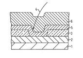
- the reference numeral 1 is the substrate containing the n + or p + doped region 2 and the substrate 3 denotes the contact hole containing SiO 2 layer.
- a tantalum disilicide layer 5 is applied in a layer thickness of 100 to 500 nm, the deposition being controlled so that more tantalum is deposited than tantalum disilicide stoichiometry. This is done, for example, by using a tantalum silicide target made of an alloy with an excess of tantalum.
- a doped layer of aluminum 6 is a layer thickness of 500 on the tantalum silicide layer 5 - evaporated nm 2000 and this double layer (5, 6) together then patterned (in the figure not shown).
- the aluminum layer 6 serves to minimize the interconnect resistance and enables problem-free contacting.
- the tantalum silicide layer 5 acts simultaneously as a diffusion barrier and as a contact material. This is possible because tantalum silicide can be used to produce ohmic contacts from n + and p + silicon and the Schottky barrier to n-silicon is sufficiently low at 0.59 eV, and secondly tantalum silicide with a higher tantalum content than tantalum disilicide Stoichiometry corresponds to the aluminum diffusion prevented during tempering steps.
Landscapes
- Engineering & Computer Science (AREA)
- Microelectronics & Electronic Packaging (AREA)
- Power Engineering (AREA)
- Physics & Mathematics (AREA)
- Condensed Matter Physics & Semiconductors (AREA)
- General Physics & Mathematics (AREA)
- Computer Hardware Design (AREA)
- Ceramic Engineering (AREA)
- Manufacturing & Machinery (AREA)
- Electrodes Of Semiconductors (AREA)
- Internal Circuitry In Semiconductor Integrated Circuit Devices (AREA)
Priority Applications (1)
| Application Number | Priority Date | Filing Date | Title |
|---|---|---|---|
| AT84108239T ATE31846T1 (de) | 1983-07-20 | 1984-07-12 | Integrierte halbleiterschaltung mit einer aus aluminium oder aus einer aluminiumlegierung bestehenden aeusseren kontaktleiterbahnebene. |
Applications Claiming Priority (2)
| Application Number | Priority Date | Filing Date | Title |
|---|---|---|---|
| DE19833326142 DE3326142A1 (de) | 1983-07-20 | 1983-07-20 | Integrierte halbleiterschaltung mit einer aus aluminium oder aus einer aluminiumlegierung bestehenden aeusseren kontaktleiterbahnebene |
| DE3326142 | 1983-07-20 |
Publications (2)
| Publication Number | Publication Date |
|---|---|
| EP0132720A1 true EP0132720A1 (fr) | 1985-02-13 |
| EP0132720B1 EP0132720B1 (fr) | 1988-01-07 |
Family
ID=6204449
Family Applications (1)
| Application Number | Title | Priority Date | Filing Date |
|---|---|---|---|
| EP84108239A Expired EP0132720B1 (fr) | 1983-07-20 | 1984-07-12 | Circuit semi-conducteur intégré comprenant une couche de contact et d'interconnexion extérieure en aluminium ou en un alliage d'aluminium |
Country Status (7)
| Country | Link |
|---|---|
| US (1) | US4912543A (fr) |
| EP (1) | EP0132720B1 (fr) |
| JP (1) | JPH0652788B2 (fr) |
| AT (1) | ATE31846T1 (fr) |
| CA (1) | CA1217574A (fr) |
| DE (2) | DE3326142A1 (fr) |
| HK (1) | HK84592A (fr) |
Cited By (12)
| Publication number | Priority date | Publication date | Assignee | Title |
|---|---|---|---|---|
| EP0199078A1 (fr) * | 1985-04-11 | 1986-10-29 | Siemens Aktiengesellschaft | Circuit intégré à semi-conducteur comprenant une voie conductrice de contact en aluminium ou en alliage d'aluminium et une couche intermédiaire en siliciure de tantale comme barrière de diffusion |
| EP0199030A2 (fr) * | 1985-04-11 | 1986-10-29 | Siemens Aktiengesellschaft | Procédé pour fabriquer des interconnexions multicouches pour des circuits intégrés à semi-conducteur comprenant au moins une couche en alliage d'aluminium avec un remplissage du trou de contact |
| EP0244995A2 (fr) * | 1986-05-02 | 1987-11-11 | Advanced Micro Devices, Inc. | Contact métallique à basse résistance pour dispositifs en silicium |
| EP0488628A2 (fr) * | 1990-11-30 | 1992-06-03 | STMicroelectronics, Inc. | Méthode de fabrication d'un trou de liaison/contact empilées en aluminium pour des interconnexions à multi-couches |
| FR2679069A1 (fr) * | 1991-07-08 | 1993-01-15 | Samsung Electronics Co Ltd | Dispositif a semiconducteur comportant une couche d'interconnexion et procede de fabrication de celui-ci. |
| US5374592A (en) * | 1992-09-22 | 1994-12-20 | Sgs-Thomson Microelectronics, Inc. | Method for forming an aluminum metal contact |
| US5472912A (en) * | 1989-11-30 | 1995-12-05 | Sgs-Thomson Microelectronics, Inc. | Method of making an integrated circuit structure by using a non-conductive plug |
| US5658828A (en) * | 1989-11-30 | 1997-08-19 | Sgs-Thomson Microelectronics, Inc. | Method for forming an aluminum contact through an insulating layer |
| US6242811B1 (en) | 1989-11-30 | 2001-06-05 | Stmicroelectronics, Inc. | Interlevel contact including aluminum-refractory metal alloy formed during aluminum deposition at an elevated temperature |
| US6271137B1 (en) | 1989-11-30 | 2001-08-07 | Stmicroelectronics, Inc. | Method of producing an aluminum stacked contact/via for multilayer |
| US6287963B1 (en) | 1990-11-05 | 2001-09-11 | Stmicroelectronics, Inc. | Method for forming a metal contact |
| US6617242B1 (en) | 1989-11-30 | 2003-09-09 | Stmicroelectronics, Inc. | Method for fabricating interlevel contacts of aluminum/refractory metal alloys |
Families Citing this family (17)
| Publication number | Priority date | Publication date | Assignee | Title |
|---|---|---|---|---|
| JP2659714B2 (ja) * | 1987-07-21 | 1997-09-30 | 株式会社日立製作所 | 半導体集積回路装置 |
| JPS6459954A (en) * | 1987-08-31 | 1989-03-07 | Nec Corp | Semiconductor integrated circuit |
| JP2895166B2 (ja) * | 1990-05-31 | 1999-05-24 | キヤノン株式会社 | 半導体装置の製造方法 |
| US5135878A (en) * | 1990-08-28 | 1992-08-04 | Solid State Devices, Inc. | Schottky diode |
| KR0123185B1 (ko) * | 1991-09-30 | 1997-11-26 | 다니이 아끼오 | 알루미늄배선 및 그 형성방법 |
| KR950003233B1 (ko) * | 1992-05-30 | 1995-04-06 | 삼성전자 주식회사 | 이중층 실리사이드 구조를 갖는 반도체 장치 및 그 제조방법 |
| US5614437A (en) * | 1995-01-26 | 1997-03-25 | Lsi Logic Corporation | Method for fabricating reliable metallization with Ta-Si-N barrier for semiconductors |
| KR100463597B1 (ko) * | 1997-09-29 | 2005-02-28 | 주식회사 하이닉스반도체 | 반도체소자의제조방법 |
| US20020132473A1 (en) * | 2001-03-13 | 2002-09-19 | Applied Materials ,Inc. | Integrated barrier layer structure for copper contact level metallization |
| US7400042B2 (en) * | 2005-05-03 | 2008-07-15 | Rosemount Aerospace Inc. | Substrate with adhesive bonding metallization with diffusion barrier |
| US7538401B2 (en) * | 2005-05-03 | 2009-05-26 | Rosemount Aerospace Inc. | Transducer for use in harsh environments |
| US20070013014A1 (en) * | 2005-05-03 | 2007-01-18 | Shuwen Guo | High temperature resistant solid state pressure sensor |
| US7628309B1 (en) | 2005-05-03 | 2009-12-08 | Rosemount Aerospace Inc. | Transient liquid phase eutectic bonding |
| KR100700545B1 (ko) * | 2005-08-10 | 2007-03-28 | 엘지전자 주식회사 | 복수의 압축기를 구비한 공기조화기의 운전제어장치 및방법 |
| US20090032958A1 (en) * | 2007-08-03 | 2009-02-05 | Micron Technology, Inc. | Intermetallic conductors |
| EP3570317A1 (fr) * | 2018-05-17 | 2019-11-20 | IMEC vzw | Dépôt régiosélectif d'un matériau de masque |
| CN113257893A (zh) * | 2021-04-30 | 2021-08-13 | 北海惠科半导体科技有限公司 | 一种肖特基二极管及其制作方法和芯片 |
Citations (3)
| Publication number | Priority date | Publication date | Assignee | Title |
|---|---|---|---|---|
| EP0000317A1 (fr) * | 1977-06-30 | 1979-01-10 | International Business Machines Corporation | Procédé de fabrication d'une électrode en siliciure sur un substrat notamment semi-conducteur |
| EP0002731A1 (fr) * | 1977-12-27 | 1979-07-11 | International Business Machines Corporation | Structure à film mince pour une disposition de contact et procédé pour sa fabrication |
| EP0046914A2 (fr) * | 1980-08-28 | 1982-03-10 | Siemens Aktiengesellschaft | Procédé de fabrication de couches métalliques de contact alliées sur structure cristalline des surfaces semi-conductrices à l'aide de rayonnements énergétiques pulsés |
Family Cites Families (9)
| Publication number | Priority date | Publication date | Assignee | Title |
|---|---|---|---|---|
| JPS5021225A (fr) * | 1973-06-29 | 1975-03-06 | ||
| JPS5380183A (en) * | 1976-12-25 | 1978-07-15 | Fujitsu Ltd | Semiconductor device |
| JPS53114366A (en) * | 1977-03-16 | 1978-10-05 | Toshiba Corp | Semiconductor device |
| US4201999A (en) * | 1978-09-22 | 1980-05-06 | International Business Machines Corporation | Low barrier Schottky diodes |
| US4276557A (en) * | 1978-12-29 | 1981-06-30 | Bell Telephone Laboratories, Incorporated | Integrated semiconductor circuit structure and method for making it |
| JPS55165680A (en) * | 1979-06-12 | 1980-12-24 | Chiyou Lsi Gijutsu Kenkyu Kumiai | Preparation of metal gate field effect device |
| JPS5669844A (en) * | 1979-11-10 | 1981-06-11 | Toshiba Corp | Manufacture of semiconductor device |
| JPS571241A (en) * | 1980-06-03 | 1982-01-06 | Toshiba Corp | Integrated circuit device |
| US4389257A (en) * | 1981-07-30 | 1983-06-21 | International Business Machines Corporation | Fabrication method for high conductivity, void-free polysilicon-silicide integrated circuit electrodes |
-
1983
- 1983-07-20 DE DE19833326142 patent/DE3326142A1/de not_active Withdrawn
-
1984
- 1984-03-22 US US06/592,403 patent/US4912543A/en not_active Expired - Lifetime
- 1984-07-12 EP EP84108239A patent/EP0132720B1/fr not_active Expired
- 1984-07-12 DE DE8484108239T patent/DE3468590D1/de not_active Expired
- 1984-07-12 AT AT84108239T patent/ATE31846T1/de not_active IP Right Cessation
- 1984-07-18 CA CA000459106A patent/CA1217574A/fr not_active Expired
- 1984-07-19 JP JP59150458A patent/JPH0652788B2/ja not_active Expired - Fee Related
-
1992
- 1992-10-29 HK HK845/92A patent/HK84592A/xx not_active IP Right Cessation
Patent Citations (3)
| Publication number | Priority date | Publication date | Assignee | Title |
|---|---|---|---|---|
| EP0000317A1 (fr) * | 1977-06-30 | 1979-01-10 | International Business Machines Corporation | Procédé de fabrication d'une électrode en siliciure sur un substrat notamment semi-conducteur |
| EP0002731A1 (fr) * | 1977-12-27 | 1979-07-11 | International Business Machines Corporation | Structure à film mince pour une disposition de contact et procédé pour sa fabrication |
| EP0046914A2 (fr) * | 1980-08-28 | 1982-03-10 | Siemens Aktiengesellschaft | Procédé de fabrication de couches métalliques de contact alliées sur structure cristalline des surfaces semi-conductrices à l'aide de rayonnements énergétiques pulsés |
Non-Patent Citations (2)
| Title |
|---|
| CHEMICAL ABSTRACTS, Band 97, 1982, Seite 705, Nr. 173139h, Columbus, Ohio, USA; W.I. LEHRER et al.: "Low-temperature LPCVD deposition of tantalum silicide" & PROC. - ELECTROCHEM. SOC. 1982, 82-87(VLSI SCI. TECHNOL.), 258-264 * |
| IBM TECHNICAL DISCLOSURE BULLETIN, Band 19, Nr. 9, Februar 1977, Seite 3382, New York, USA; P.L. GARBARINO et al.: "Contact barrier metallurgy for MOSFET gate" * |
Cited By (19)
| Publication number | Priority date | Publication date | Assignee | Title |
|---|---|---|---|---|
| EP0199078A1 (fr) * | 1985-04-11 | 1986-10-29 | Siemens Aktiengesellschaft | Circuit intégré à semi-conducteur comprenant une voie conductrice de contact en aluminium ou en alliage d'aluminium et une couche intermédiaire en siliciure de tantale comme barrière de diffusion |
| EP0199030A2 (fr) * | 1985-04-11 | 1986-10-29 | Siemens Aktiengesellschaft | Procédé pour fabriquer des interconnexions multicouches pour des circuits intégrés à semi-conducteur comprenant au moins une couche en alliage d'aluminium avec un remplissage du trou de contact |
| US4680612A (en) * | 1985-04-11 | 1987-07-14 | Siemens Aktiengesellschaft | Integrated semiconductor circuit including a tantalum silicide diffusion barrier |
| EP0199030A3 (fr) * | 1985-04-11 | 1987-08-26 | Siemens Aktiengesellschaft | Procédé pour fabriquer des interconnexions multicouches pour des circuits intégrés à semi-conducteur comprenant au moins une couche en alliage d'aluminium avec un remplissage du trou de contact |
| EP0244995A2 (fr) * | 1986-05-02 | 1987-11-11 | Advanced Micro Devices, Inc. | Contact métallique à basse résistance pour dispositifs en silicium |
| EP0244995A3 (en) * | 1986-05-02 | 1988-05-04 | Advanced Micro Devices, Inc. | Low resistance metal contact for silicon devices |
| US5658828A (en) * | 1989-11-30 | 1997-08-19 | Sgs-Thomson Microelectronics, Inc. | Method for forming an aluminum contact through an insulating layer |
| US5472912A (en) * | 1989-11-30 | 1995-12-05 | Sgs-Thomson Microelectronics, Inc. | Method of making an integrated circuit structure by using a non-conductive plug |
| US5976969A (en) * | 1989-11-30 | 1999-11-02 | Stmicroelectronics, Inc. | Method for forming an aluminum contact |
| US6242811B1 (en) | 1989-11-30 | 2001-06-05 | Stmicroelectronics, Inc. | Interlevel contact including aluminum-refractory metal alloy formed during aluminum deposition at an elevated temperature |
| US6271137B1 (en) | 1989-11-30 | 2001-08-07 | Stmicroelectronics, Inc. | Method of producing an aluminum stacked contact/via for multilayer |
| US6617242B1 (en) | 1989-11-30 | 2003-09-09 | Stmicroelectronics, Inc. | Method for fabricating interlevel contacts of aluminum/refractory metal alloys |
| US6287963B1 (en) | 1990-11-05 | 2001-09-11 | Stmicroelectronics, Inc. | Method for forming a metal contact |
| EP0488628A3 (en) * | 1990-11-30 | 1992-11-04 | Sgs-Thomson Microelectronics, Inc. | Method of producing an aluminum stacked contact/via for multilayer interconnections |
| EP0488628A2 (fr) * | 1990-11-30 | 1992-06-03 | STMicroelectronics, Inc. | Méthode de fabrication d'un trou de liaison/contact empilées en aluminium pour des interconnexions à multi-couches |
| FR2679069A1 (fr) * | 1991-07-08 | 1993-01-15 | Samsung Electronics Co Ltd | Dispositif a semiconducteur comportant une couche d'interconnexion et procede de fabrication de celui-ci. |
| US5355020A (en) * | 1991-07-08 | 1994-10-11 | Samsung Electronics Co., Ltd. | Semiconductor device having a multi-layer metal contact |
| US5374592A (en) * | 1992-09-22 | 1994-12-20 | Sgs-Thomson Microelectronics, Inc. | Method for forming an aluminum metal contact |
| US6433435B2 (en) | 1993-11-30 | 2002-08-13 | Stmicroelectronics, Inc. | Aluminum contact structure for integrated circuits |
Also Published As
| Publication number | Publication date |
|---|---|
| JPS6039866A (ja) | 1985-03-01 |
| DE3468590D1 (en) | 1988-02-11 |
| JPH0652788B2 (ja) | 1994-07-06 |
| EP0132720B1 (fr) | 1988-01-07 |
| HK84592A (en) | 1992-11-06 |
| ATE31846T1 (de) | 1988-01-15 |
| CA1217574A (fr) | 1987-02-03 |
| US4912543A (en) | 1990-03-27 |
| DE3326142A1 (de) | 1985-01-31 |
Similar Documents
| Publication | Publication Date | Title |
|---|---|---|
| EP0132720B1 (fr) | Circuit semi-conducteur intégré comprenant une couche de contact et d'interconnexion extérieure en aluminium ou en un alliage d'aluminium | |
| DE69929496T2 (de) | Struktur für Kupferleitungsverbindungsleitung, die eine metallische Keimschicht umfasst | |
| EP0090318B1 (fr) | Procédé pour la formation de circuits intégrés à transistors à effet de champ MOS utilisant la technologie d'électrode de porte en silicium ayant des couches de siliciures sur des régions diffusées utilisées comme conducteurs | |
| DE69837674T2 (de) | Doppeldamaszen-metallisierung | |
| DE4200809C2 (de) | Verfahren zur Bildung einer metallischen Verdrahtungsschicht in einem Halbleiterbauelement | |
| EP0269095B1 (fr) | Circuit intégré à semi-conducteur ayant au moins deux plans métallisés en aluminium ou en alliage d'aluminium ainsi que son procédé de fabrication | |
| DE69637333T2 (de) | Kupferlegierungen für Chipverbindungen und Herstellungsverfahren | |
| DE10196065B3 (de) | Verbindungsstruktur für eine integrierte Schaltung, Verfahren zur Herstellung der Verbindungsstruktur und integrierte Schaltung mit der Verbindungsstruktur | |
| EP0123309B1 (fr) | Procédé pour fabriquer des contacts stables à basse résistance dans des circuits semi-conducteurs intégrés | |
| EP0199078B1 (fr) | Circuit intégré à semi-conducteur comprenant une voie conductrice de contact en aluminium ou en alliage d'aluminium et une couche intermédiaire en siliciure de tantale comme barrière de diffusion | |
| EP0304728A2 (fr) | Procédé de fabrication d'une métallisation plane de faible résistance en aluminium ou en alliage d'aluminium | |
| DE4342047A1 (de) | Halbleiterbauelement und Verfahren zu seiner Herstellung | |
| DE4400200A1 (de) | Halbleitervorrichtung | |
| DE4010618A1 (de) | Halbleitervorrichtung und verfahren zu ihrer herstellung | |
| DE19608208B4 (de) | Verfahren zur Herstellung von Metallzwischenverbindungen in Halbleitereinrichtungen | |
| DE3414781A1 (de) | Vielschicht-verbindungsstruktur einer halbleitereinrichtung | |
| DE4239457C2 (de) | Halbleiterwaferstruktur und Herstellungsverfahren dafür | |
| DE19645033C2 (de) | Verfahren zur Bildung eines Metalldrahtes | |
| DE4244115C2 (de) | Halbleitervorrichtung und Verfahren zum Herstellen der Halbleitervorrichtung | |
| DE4238080C2 (de) | Verbindungsstruktur für leitende Schichten einer Halbleitervorrichtung und ein Verfahren zu deren Herstellung | |
| EP1665371B1 (fr) | Procede pour realiser une couche dielectrique multifonctionnelle sur un substrat | |
| EP0134571B1 (fr) | Circuit semi-conducteur intégré ayant une métallisation multicouche en aluminium ou en alliage d'aluminium et procédé pour sa fabrication | |
| EP0448763A1 (fr) | Procédé et appareil pour la fabrication de couches ou structures conductrices pour circuits semi-conducteurs ayant la plus haute densité d'intégration | |
| DE102004063149B4 (de) | Verfahren zur Herstellung eines Halbleiter-Bauelements | |
| DE60215221T2 (de) | Verfahren zur herstellung einer elektronischen einrichtung |
Legal Events
| Date | Code | Title | Description |
|---|---|---|---|
| PUAI | Public reference made under article 153(3) epc to a published international application that has entered the european phase |
Free format text: ORIGINAL CODE: 0009012 |
|
| 17P | Request for examination filed |
Effective date: 19841128 |
|
| AK | Designated contracting states |
Designated state(s): AT CH DE FR GB IT LI NL SE |
|
| 17Q | First examination report despatched |
Effective date: 19860207 |
|
| R17C | First examination report despatched (corrected) |
Effective date: 19860704 |
|
| GRAA | (expected) grant |
Free format text: ORIGINAL CODE: 0009210 |
|
| AK | Designated contracting states |
Kind code of ref document: B1 Designated state(s): AT CH DE FR GB IT LI NL SE |
|
| REF | Corresponds to: |
Ref document number: 31846 Country of ref document: AT Date of ref document: 19880115 Kind code of ref document: T |
|
| REF | Corresponds to: |
Ref document number: 3468590 Country of ref document: DE Date of ref document: 19880211 |
|
| ET | Fr: translation filed | ||
| ITF | It: translation for a ep patent filed |
Owner name: STUDIO JAUMANN |
|
| GBT | Gb: translation of ep patent filed (gb section 77(6)(a)/1977) | ||
| PLBE | No opposition filed within time limit |
Free format text: ORIGINAL CODE: 0009261 |
|
| STAA | Information on the status of an ep patent application or granted ep patent |
Free format text: STATUS: NO OPPOSITION FILED WITHIN TIME LIMIT |
|
| 26N | No opposition filed | ||
| ITTA | It: last paid annual fee | ||
| PGFP | Annual fee paid to national office [announced via postgrant information from national office to epo] |
Ref country code: SE Payment date: 19910731 Year of fee payment: 8 |
|
| PGFP | Annual fee paid to national office [announced via postgrant information from national office to epo] |
Ref country code: CH Payment date: 19911030 Year of fee payment: 8 |
|
| PG25 | Lapsed in a contracting state [announced via postgrant information from national office to epo] |
Ref country code: SE Effective date: 19920713 |
|
| PG25 | Lapsed in a contracting state [announced via postgrant information from national office to epo] |
Ref country code: LI Effective date: 19920731 Ref country code: CH Effective date: 19920731 |
|
| REG | Reference to a national code |
Ref country code: CH Ref legal event code: PL |
|
| EUG | Se: european patent has lapsed |
Ref document number: 84108239.9 Effective date: 19930204 |
|
| PGFP | Annual fee paid to national office [announced via postgrant information from national office to epo] |
Ref country code: AT Payment date: 19960621 Year of fee payment: 13 |
|
| PGFP | Annual fee paid to national office [announced via postgrant information from national office to epo] |
Ref country code: NL Payment date: 19960716 Year of fee payment: 13 |
|
| PG25 | Lapsed in a contracting state [announced via postgrant information from national office to epo] |
Ref country code: AT Free format text: LAPSE BECAUSE OF NON-PAYMENT OF DUE FEES Effective date: 19970712 |
|
| PG25 | Lapsed in a contracting state [announced via postgrant information from national office to epo] |
Ref country code: NL Free format text: LAPSE BECAUSE OF NON-PAYMENT OF DUE FEES Effective date: 19980201 |
|
| NLV4 | Nl: lapsed or anulled due to non-payment of the annual fee |
Effective date: 19980201 |
|
| REG | Reference to a national code |
Ref country code: GB Ref legal event code: IF02 |
|
| PGFP | Annual fee paid to national office [announced via postgrant information from national office to epo] |
Ref country code: GB Payment date: 20030704 Year of fee payment: 20 |
|
| PGFP | Annual fee paid to national office [announced via postgrant information from national office to epo] |
Ref country code: FR Payment date: 20030711 Year of fee payment: 20 |
|
| PGFP | Annual fee paid to national office [announced via postgrant information from national office to epo] |
Ref country code: DE Payment date: 20030915 Year of fee payment: 20 |
|
| PG25 | Lapsed in a contracting state [announced via postgrant information from national office to epo] |
Ref country code: GB Free format text: LAPSE BECAUSE OF EXPIRATION OF PROTECTION Effective date: 20040711 |
|
| REG | Reference to a national code |
Ref country code: GB Ref legal event code: PE20 |