EP0116440B1 - Integrated semiconductor circuit device for generating a switching control signal - Google Patents
Integrated semiconductor circuit device for generating a switching control signal Download PDFInfo
- Publication number
- EP0116440B1 EP0116440B1 EP84300648A EP84300648A EP0116440B1 EP 0116440 B1 EP0116440 B1 EP 0116440B1 EP 84300648 A EP84300648 A EP 84300648A EP 84300648 A EP84300648 A EP 84300648A EP 0116440 B1 EP0116440 B1 EP 0116440B1
- Authority
- EP
- European Patent Office
- Prior art keywords
- circuits
- circuit
- switching
- redundant
- regular
- Prior art date
- Legal status (The legal status is an assumption and is not a legal conclusion. Google has not performed a legal analysis and makes no representation as to the accuracy of the status listed.)
- Expired
Links
Images

Classifications
-
- G—PHYSICS
- G11—INFORMATION STORAGE
- G11C—STATIC STORES
- G11C29/00—Checking stores for correct operation ; Subsequent repair; Testing stores during standby or offline operation
-
- G—PHYSICS
- G11—INFORMATION STORAGE
- G11C—STATIC STORES
- G11C29/00—Checking stores for correct operation ; Subsequent repair; Testing stores during standby or offline operation
- G11C29/70—Masking faults in memories by using spares or by reconfiguring
- G11C29/78—Masking faults in memories by using spares or by reconfiguring using programmable devices
- G11C29/785—Masking faults in memories by using spares or by reconfiguring using programmable devices with redundancy programming schemes
- G11C29/789—Masking faults in memories by using spares or by reconfiguring using programmable devices with redundancy programming schemes using non-volatile cells or latches
-
- G—PHYSICS
- G11—INFORMATION STORAGE
- G11C—STATIC STORES
- G11C29/00—Checking stores for correct operation ; Subsequent repair; Testing stores during standby or offline operation
- G11C29/70—Masking faults in memories by using spares or by reconfiguring
- G11C29/78—Masking faults in memories by using spares or by reconfiguring using programmable devices
- G11C29/83—Masking faults in memories by using spares or by reconfiguring using programmable devices with reduced power consumption
Definitions
- the present invention relates to an integrated semiconductor circuit device, more particularly, it relates to an integrated semiconductor device for generating a switching control signal.
- the device according to the present invention can be used for a semiconductor memory device with a redundant circuit, such as, for example, an erasable programmable read only memory (EPROM) with a redundant circuit.
- EPROM erasable programmable read only memory
- memory cell arrays for nine bits including one redundant memory cell array are provided.
- the first to the eighth memory cell arrays are the regular memory cell arrays, while the ninth memory cell array is the redundant memory cell array.
- the ninth memory cell array is connected in place of the failed regular memory cell array, so that the normal operation of the device is maintained.
- This switching of the connection from the regular memory cell array to the redundant memory cell array is carried out by a switching control signal generation circuit.
- the function of this curcuit is to decide whether a fuse should be in a conductive or nonconductive state.
- the peripheral circuits constituted by complementary MOS field effect transistors around a semiconductor memory device have the advantage of low power consumption.
- the current in such peripheral circuits can be reduced to the order of 10- 9 A.
- the current flowing through the pull-down resistor tends to be increased to the order of 10- 6 A, and may reach up to 50 x 10- 6 A. If such a current flows in the circuit, the advantage of using complementary MOS field effect transistors will be lost, and the advantage of using a redundant circuit cannot be fully appreciated.
- a 16-K Static RAM having normal columns and a spare coluumn. Additional decoders in the form of NOR gates are provided for deciding whether the spare column is to be activated in place of one of the normal columns.
- the decoders receive incoming address signals, and output signals from fused latches.
- the fused latches each comprise a fuse, a two-transistor latch, and an "exclusive-NOR" gate receiving incoming address signals; when the fuse is unblown there is still one power-consuming stage.
- an integrated semiconductor circuit device comprising a plurality of regular integrated semiconductor circuits and a redundant integrated semiconductor circuit, and having selecting means for selecting operation of the redundant circuit when one of the regular circuits is faulty, the selecting means comprising switching control signal generation circuits for generating switching control signals and each having a flip-flop circuit and a fuse having one terminal for connection to a power source and the other terminal connected to said flip-flop circuit; fuse blowing means; and switching circuits responsive to the switching control signals; characterised by
- an improved semiconductor integrated circuit device e.g. a memory device
- a reduntant circuit in which the current flowing through the switching control signal generation circuit for the redundant circuit is reduced, and the power consumption in the switching control signal generation circuit for the redundant circuit is also reduced, maintaining the advantage of the use of complementary MOS field effect transistors.
- a semiconductor integrated circuit device in which there is a simple correspondence between the state of a fuse in a switching control signal generation circuit, and the replacement or non-replacement of a regular circuit by a redundant circuit.
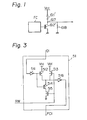
- FIG. 1 An example of a prior art switching control signal generation circuit is shown in Fig. 1.
- the circuit shown in Fig. 1 includes a fuse 611', a fuse blowing control circuit FC, an N-channel field effect transistor 612', and a pull-down resistor 618.
- One terminal of the fuse 611' is connected to the voltage source V cc , while the other terminal is connected to the drain of an N-channel field effect transistor 612' and one terminal of the pull-down resistor 618.
- the output of the fuse blowing control circuit FC is supplied to the gate of the transistor 612'.
- the source of the transistor 612' is grounded, and the output of the switching control signal generation circuit is produced from the junction 617 of the fuse 611' and the transistor 612'.
- the fuse 611' made of polycrystalline silicon, is blown when the N-channel field effect transistor 612' becomes ON. Hence, when the fuse 611' is not blown, the voltage of the junction 617 is equal to V cc , while when the fuse 611' is blown, the voltage of the junction 617 is that of ground.
- the output of the switching control signal generation circuit shown in Fig. 1 is used for controlling the switching to the redundant memory cell array in such a manner that the blowing of the fuse 611' causes the switching from a failure memory cell array to the redundant memory cell array.
- the peripheral circuits constituted by complementary MOS field effect transistors used around a semiconductor memory device have the advantage of a lower power consumption.
- the current in such peripheral circuits can be reduced to the order of 10- 9 A.
- the current flowing through the pull-down resistor 618 tends to be increased to the order of 10- 6 A, and may reach up to 50 x 10- 6 A. If a current of such an order flows in the circuit, the advantage of using complementary MOS field effect transistors will be lost, and at the same time, the advantage of using the redundant circuit cannot be appreciated.
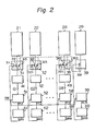
- FIG. 2 A semiconductor memory device with a redundant circuit according to an embodiment of the present invention is illustrated in Fig. 2.
- the semiconductor memory device shown in Fig. 2 is an erasable programmable read only memory (EPROM) type. This device is provided with eight regular memory cell arrays 21, 22,... 28 and one redundant memory cell array 29.
- the device is also provided with switching circuits 31,32, ...38 corresponding to the regular memory cell arrays 21,22,... 28, a switching circuit 39 corresponding to the redundant memory cell array 29, and output buffer circuits 41, 42,...48 corresponding to the switching circuits 31, 32, ... 38.
- Eight bit data Q1, Q2, ... Q8 from an address of the memory cell arrays are obtained at output terminals of the output buffer circuits 41, 42, ... 48.
- the output terminals of the output buffer circuits 41, 42,...48 are connected to the Q1, Q2, ... Q8 input terminals of the fuse blowing control circuits 51, 52, ... 58.
- the output terminals of the fuse blowing control circuits 51, 52, ... 58 are connected to the FC1, FC2, ... FC8 input terminals of the switching control signal generation circuits 61, 62, ... 68.
- the output terminal of the fuse blowing control circuit 59 is connected to the FC9 input terminal of the switching control signal generation circuit 69.
- the output of the redundant memory cell array 29 is adapted to be connected to the switching circuits 31, 32, ... 38 corresponding to the regular memory cell arrays, via the switching circuit 39 corresponding to the redundant memory cell array.
- Each of the switching circuits 31, 32,... 38 includes an inverter (311, 321, ... 381 a a first field effect transistor (312, 322, ... 382), and a second field effect transistor (313, 323, ... 383).
- the switching circuit 39 includes a field effect transistor 391.
- the switching control signals BR1, BR2,.... BR8 produced from switching control signal generation circuits 61, 62, ... 68 are supplied to the switching circuits 31, 32, ... 38, whle the switching control signal BR9 produced from a switching control signal generation circuit 69 is supplied to the switching circuit 39.
- the replacement of the output of a selected regular memory cell array, for example, 21, by the output of the redundant memory cell array 29 is carried out as follows.
- the replacement is instructed by setting the potential of the redundant control signal RW, supplied to the fuse blowing control circuits 51, 52, ... 59, to be HIGH, and setting the potential of the Q1 input of the fuse blowing control circuit 51 to be LOW, by an external means.
- the potential of the FC1 output signal from the fuse blowing control circuit 51 becomes HIGH, and the potential of the FC9 output signal-from the fuse blowing control circuit 59 also becomes HIGH.
- a HIGH FC1 signal is supplied to the switching control signal generation circuit 61 and a HIGH FC9 signal is supplied to the switching control signal generation circuit 69
- the fuses in the switching control signal generation circuits 61 and 69 are blown, and hence both potentials of the output signals BR1 and BR9 of the switching control signal generation circuits 61 and 69 become HIGH.
- the output of the redundant memory cell array 29 is supplied via the switching circuit 39 and the switching circuit 31 to the output buffer circuit 41, while the outputs of the regular memory cell arrays 22, ... 28 are supplied via the switching circuits 32, ... 38 to the output buffer circuits 42, ... 48.
- the replacement of the output of the regular memory cell array 21 by the output of the redundant memory cell array 29 is achieved.
- the fuse blowing control circuits 51, 52, ... 58 have the same structure; for example, the structure of the fuse blowing control circuit 51 illustrated in Fig. 3.
- the structure of the fuse blowing control circuit 59 is illustrated in Fig. 4.
- the fuse blowing control circuit 51 includes an inverter 511, field effect transistors 512, 513, 514, and 515, and an inverter 516.
- the fuse blowing control circuit 59 includes a waveform shaper consisting of two inverters formed by field effect transistors 591, 592, 593, and 594.
- the fuse blowing control circuit 51 produces a HIGH FC1 output signal. If the potential of the redundant control signal RW is made HIGH, the fuse blowing control circuit 59 produces a HIGH FC9 output signal.
- the switching control signal generation circuits 61, 62, ... 69 have the same structure; for example, the structure of the switching control signal generation circuit 61 illustrated in Fig. 5.
- the switching control signal generation circuit 61 includes a fuse 611, a field effect transistor 612, a capacitor 613, a flip-flop unit 614 consisting of two complementary MOS field effect transistor type inverters formed by MOS field effect transistors 614a, 614b, 614c, and 614d, and a capacitor 615.
- a fuse 611 When the fuse 611 is not blown the potential of the output signal BR1 is LOW, while when the fuse 611 is blown the potential of the output signal BR1 is HIGH.
- the capacitors 613 and 615 are provided for ensuring the HIGH potential of the output signal BR1 when the power source is switched on where the fuse 611 is blown. It is desirable to select the conductance of the field effect transistor 614a to be small in order to further ensure the HIGH potential of the output signal BR1 when the power source is switched on where the fuse 611 is blown.
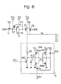
- a power source having a relatively low voltage V ee of, for example, 5 V, for melting the fuse it is also possible to use an additional power source having a relatively high voltage Vpp of, for example, 21 V, as shown in Fig. 6.
- Vpp relatively high voltage
- the transistors 72 and 75 expressed by the transistor symbol having an angle mark have a high withstand voltage.
- the transistor 76 is in the OFF state.
- the potential of the output of the inverter consisting of the transistors 73 and 74 becomes HIGH.
- the transistor 75 becomes conductive, and accordingly, the voltage V 6 becomes equal to Vpp-
- the blowing of the fuse is easily carried out when the potential of the signal FC1 is made HIGH.
- the potential of the signal RW is usually HIGH. Therefore, the transistor 76 becomes conductive, and the output of the inverter formed by transistors 73 and 74 becomes LOW. Hence, the transistor 75 enters the OFF state, and the transistor 76 enters the ON state. Accordingly, the voltage V 6 becomes equal to V ee .
- the operation of the circuit 61 is the same as in the case of Fig. 4.
- the present invention is applicable not only to an EPROM, but also to an integrated circuit for a random access memory, an integrated circuit for a logic circuit, or the like.
Landscapes
- For Increasing The Reliability Of Semiconductor Memories (AREA)
- Design And Manufacture Of Integrated Circuits (AREA)
- Techniques For Improving Reliability Of Storages (AREA)
Applications Claiming Priority (2)
| Application Number | Priority Date | Filing Date | Title |
|---|---|---|---|
| JP16273/83 | 1983-02-04 | ||
| JP58016273A JPS59142800A (ja) | 1983-02-04 | 1983-02-04 | 半導体集積回路装置 |
Publications (3)
| Publication Number | Publication Date |
|---|---|
| EP0116440A2 EP0116440A2 (en) | 1984-08-22 |
| EP0116440A3 EP0116440A3 (en) | 1986-05-14 |
| EP0116440B1 true EP0116440B1 (en) | 1990-05-23 |
Family
ID=11911933
Family Applications (1)
| Application Number | Title | Priority Date | Filing Date |
|---|---|---|---|
| EP84300648A Expired EP0116440B1 (en) | 1983-02-04 | 1984-02-02 | Integrated semiconductor circuit device for generating a switching control signal |
Country Status (7)
| Country | Link |
|---|---|
| US (1) | US4614881A (en:Method) |
| EP (1) | EP0116440B1 (en:Method) |
| JP (1) | JPS59142800A (en:Method) |
| KR (1) | KR900001740B1 (en:Method) |
| CA (1) | CA1208310A (en:Method) |
| DE (1) | DE3482343D1 (en:Method) |
| IE (1) | IE55824B1 (en:Method) |
Families Citing this family (23)
| Publication number | Priority date | Publication date | Assignee | Title |
|---|---|---|---|---|
| FR2576132B1 (fr) * | 1985-01-15 | 1990-06-29 | Eurotechnique Sa | Memoire en circuit integre |
| US4689494A (en) * | 1986-09-18 | 1987-08-25 | Advanced Micro Devices, Inc. | Redundancy enable/disable circuit |
| JPH0677400B2 (ja) * | 1987-11-12 | 1994-09-28 | シャープ株式会社 | 半導体集積回路装置 |
| NL8800846A (nl) * | 1988-04-05 | 1989-11-01 | Philips Nv | Geintegreerde schakeling met een programmeerbare cel. |
| US5204990A (en) * | 1988-09-07 | 1993-04-20 | Texas Instruments Incorporated | Memory cell with capacitance for single event upset protection |
| JPH0289299A (ja) * | 1988-09-27 | 1990-03-29 | Nec Corp | 半導体記憶装置 |
| US4908525A (en) * | 1989-02-03 | 1990-03-13 | The United States Of America As Represented By The Secretary Of The Air Force | Cut-only CMOS switch for discretionary connect and disconnect |
| JPH07105159B2 (ja) * | 1989-11-16 | 1995-11-13 | 株式会社東芝 | 半導体記憶装置の冗長回路 |
| US5038368A (en) * | 1990-02-02 | 1991-08-06 | David Sarnoff Research Center, Inc. | Redundancy control circuit employed with various digital logic systems including shift registers |
| JP3001252B2 (ja) * | 1990-11-16 | 2000-01-24 | 株式会社日立製作所 | 半導体メモリ |
| JPH0831279B2 (ja) * | 1990-12-20 | 1996-03-27 | インターナショナル・ビジネス・マシーンズ・コーポレイション | 冗長システム |
| FR2684206B1 (fr) * | 1991-11-25 | 1994-01-07 | Sgs Thomson Microelectronics Sa | Circuit de lecture de fusible de redondance pour memoire integree. |
| US5319592A (en) * | 1992-11-25 | 1994-06-07 | Fujitsu Limited | Fuse-programming circuit |
| US5440246A (en) * | 1994-03-22 | 1995-08-08 | Mosel Vitelic, Incorporated | Programmable circuit with fusible latch |
| US6100747A (en) * | 1994-05-30 | 2000-08-08 | Stmicroelectronics, S.R.L. | Device for selecting design options in an integrated circuit |
| DE69622988D1 (de) * | 1996-03-22 | 2002-09-19 | St Microelectronics Srl | Schaltung um Übereinstimmung zwischen einer darin gespeicherten binären Informationseinheit und einem einkommenden Datum festzustellen |
| IT1286037B1 (it) * | 1996-10-25 | 1998-07-07 | Sgs Thomson Microelectronics | Circuito per la abilitazione selettiva di una pluralita' di alternative circuitali di un circuito integrato |
| DE69712302T2 (de) | 1996-12-31 | 2002-10-24 | Stmicroelectronics, Inc. | Struktur und Bauelement zur Auswahl von Entwurfsmöglichkeiten in einem integrierten Schaltkreis |
| US5889414A (en) * | 1997-04-28 | 1999-03-30 | Mosel Vitelic Corporation | Programmable circuits |
| US6084803A (en) * | 1998-10-23 | 2000-07-04 | Mosel Vitelic, Inc. | Initialization of non-volatile programmable latches in circuits in which an initialization operation is performed |
| US6163492A (en) | 1998-10-23 | 2000-12-19 | Mosel Vitelic, Inc. | Programmable latches that include non-volatile programmable elements |
| US6621319B1 (en) * | 1999-09-29 | 2003-09-16 | Agere Systems Inc. | Edge-triggered toggle flip-flop circuit |
| TWI251900B (en) * | 2005-02-15 | 2006-03-21 | Neotec Semiconductor Ltd | Trimming fuse with latch circuit |
Family Cites Families (6)
| Publication number | Priority date | Publication date | Assignee | Title |
|---|---|---|---|---|
| US4228528B2 (en) * | 1979-02-09 | 1992-10-06 | Memory with redundant rows and columns | |
| JPS5685934A (en) * | 1979-12-14 | 1981-07-13 | Nippon Telegr & Teleph Corp <Ntt> | Control signal generating circuit |
| US4358833A (en) * | 1980-09-30 | 1982-11-09 | Intel Corporation | Memory redundancy apparatus for single chip memories |
| US4446534A (en) * | 1980-12-08 | 1984-05-01 | National Semiconductor Corporation | Programmable fuse circuit |
| US4546455A (en) * | 1981-12-17 | 1985-10-08 | Tokyo Shibaura Denki Kabushiki Kaisha | Semiconductor device |
| US4459685A (en) * | 1982-03-03 | 1984-07-10 | Inmos Corporation | Redundancy system for high speed, wide-word semiconductor memories |
-
1983
- 1983-02-04 JP JP58016273A patent/JPS59142800A/ja active Granted
-
1984
- 1984-01-27 CA CA000446244A patent/CA1208310A/en not_active Expired
- 1984-01-27 US US06/574,728 patent/US4614881A/en not_active Expired - Lifetime
- 1984-01-31 KR KR1019840000426A patent/KR900001740B1/ko not_active Expired
- 1984-02-02 DE DE8484300648T patent/DE3482343D1/de not_active Expired - Lifetime
- 1984-02-02 EP EP84300648A patent/EP0116440B1/en not_active Expired
- 1984-02-03 IE IE263/84A patent/IE55824B1/en not_active IP Right Cessation
Also Published As
| Publication number | Publication date |
|---|---|
| EP0116440A2 (en) | 1984-08-22 |
| US4614881A (en) | 1986-09-30 |
| DE3482343D1 (de) | 1990-06-28 |
| IE55824B1 (en) | 1991-01-30 |
| JPS59142800A (ja) | 1984-08-16 |
| KR900001740B1 (ko) | 1990-03-19 |
| CA1208310A (en) | 1986-07-22 |
| JPS6236316B2 (en:Method) | 1987-08-06 |
| IE840263L (en) | 1984-08-04 |
| KR840008075A (ko) | 1984-12-12 |
| EP0116440A3 (en) | 1986-05-14 |
Similar Documents
| Publication | Publication Date | Title |
|---|---|---|
| EP0116440B1 (en) | Integrated semiconductor circuit device for generating a switching control signal | |
| US5566107A (en) | Programmable circuit for enabling an associated circuit | |
| US5663658A (en) | Low current redundancy fuse assembly | |
| US4546455A (en) | Semiconductor device | |
| US4837747A (en) | Redundary circuit with a spare main decoder responsive to an address of a defective cell in a selected cell block | |
| EP0052481B1 (en) | Semiconductor device having a device state identifying circuit | |
| US4885721A (en) | Semiconductor memory device with redundant memory cells | |
| KR960000680B1 (ko) | 반도체 메모리 장치 | |
| KR910001533B1 (ko) | 휴즈회로와 그내의 휴즈상태 검출회로를 갖는 반도체장치 | |
| WO1981002360A1 (en) | Block redundancy for memory array | |
| US4617651A (en) | Redundancy circuit for use in a semiconductor memory array | |
| JP2006139900A (ja) | 内部発生されたプログラミング電圧を用いてアンチヒューズをプログラムする方法及び装置 | |
| US4485459A (en) | Redundant columns for byte wide memories | |
| EP0121394A2 (en) | Static semiconductor memory device incorporating redundancy memory cells | |
| JPH058520B2 (en:Method) | ||
| EP0376245A2 (en) | Semiconductors memory device provided with an improved redundant decoder | |
| US4587638A (en) | Semiconductor memory device | |
| US4829481A (en) | Defective element disabling circuit having a laser-blown fuse | |
| US5208780A (en) | Structure of electrically programmable read-only memory cells and redundancy signature therefor | |
| US5945840A (en) | Low current redundancy anti-fuse assembly | |
| EP0019381B1 (en) | Semiconductor memory device with address signal level setting | |
| US6509598B2 (en) | Semiconductor memory device having a redundant block and reduced power consumption | |
| US5952845A (en) | Semiconductor programmable test arrangement such as an antifuse ID circuit having common access switches and/or common programming switches | |
| KR100247606B1 (ko) | 효율이 개선된 dram 행 용장 회로 및 용장 대체 방법 | |
| US6333876B1 (en) | Semiconductor memory device |
Legal Events
| Date | Code | Title | Description |
|---|---|---|---|
| PUAI | Public reference made under article 153(3) epc to a published international application that has entered the european phase |
Free format text: ORIGINAL CODE: 0009012 |
|
| AK | Designated contracting states |
Designated state(s): DE FR GB |
|
| PUAL | Search report despatched |
Free format text: ORIGINAL CODE: 0009013 |
|
| AK | Designated contracting states |
Kind code of ref document: A3 Designated state(s): DE FR GB |
|
| 17P | Request for examination filed |
Effective date: 19861029 |
|
| 17Q | First examination report despatched |
Effective date: 19880229 |
|
| GRAA | (expected) grant |
Free format text: ORIGINAL CODE: 0009210 |
|
| AK | Designated contracting states |
Kind code of ref document: B1 Designated state(s): DE FR GB |
|
| ET | Fr: translation filed | ||
| REF | Corresponds to: |
Ref document number: 3482343 Country of ref document: DE Date of ref document: 19900628 |
|
| PLBE | No opposition filed within time limit |
Free format text: ORIGINAL CODE: 0009261 |
|
| STAA | Information on the status of an ep patent application or granted ep patent |
Free format text: STATUS: NO OPPOSITION FILED WITHIN TIME LIMIT |
|
| 26N | No opposition filed | ||
| PGFP | Annual fee paid to national office [announced via postgrant information from national office to epo] |
Ref country code: GB Payment date: 19921208 Year of fee payment: 10 |
|
| PGFP | Annual fee paid to national office [announced via postgrant information from national office to epo] |
Ref country code: FR Payment date: 19921229 Year of fee payment: 10 |
|
| PGFP | Annual fee paid to national office [announced via postgrant information from national office to epo] |
Ref country code: DE Payment date: 19930427 Year of fee payment: 10 |
|
| PG25 | Lapsed in a contracting state [announced via postgrant information from national office to epo] |
Ref country code: GB Effective date: 19940202 |
|
| GBPC | Gb: european patent ceased through non-payment of renewal fee |
Effective date: 19940202 |
|
| PG25 | Lapsed in a contracting state [announced via postgrant information from national office to epo] |
Ref country code: FR Effective date: 19941031 |
|
| PG25 | Lapsed in a contracting state [announced via postgrant information from national office to epo] |
Ref country code: DE Effective date: 19941101 |
|
| REG | Reference to a national code |
Ref country code: FR Ref legal event code: ST |