EP0097789A2 - Verfahren zum Füllen mit Silizium von Gräben in Halbleitersubstraten - Google Patents
Verfahren zum Füllen mit Silizium von Gräben in Halbleitersubstraten Download PDFInfo
- Publication number
- EP0097789A2 EP0097789A2 EP83104287A EP83104287A EP0097789A2 EP 0097789 A2 EP0097789 A2 EP 0097789A2 EP 83104287 A EP83104287 A EP 83104287A EP 83104287 A EP83104287 A EP 83104287A EP 0097789 A2 EP0097789 A2 EP 0097789A2
- Authority
- EP
- European Patent Office
- Prior art keywords
- trench
- nucleating material
- silicon
- nucleating
- sidewalls
- Prior art date
- Legal status (The legal status is an assumption and is not a legal conclusion. Google has not performed a legal analysis and makes no representation as to the accuracy of the status listed.)
- Granted
Links
Images

Classifications
-
- H—ELECTRICITY
- H10—SEMICONDUCTOR DEVICES; ELECTRIC SOLID-STATE DEVICES NOT OTHERWISE PROVIDED FOR
- H10P—GENERIC PROCESSES OR APPARATUS FOR THE MANUFACTURE OR TREATMENT OF DEVICES COVERED BY CLASS H10
- H10P14/00—Formation of materials, e.g. in the shape of layers or pillars
- H10P14/20—Formation of materials, e.g. in the shape of layers or pillars of semiconductor materials
- H10P14/24—Formation of materials, e.g. in the shape of layers or pillars of semiconductor materials using chemical vapour deposition [CVD]
-
- H—ELECTRICITY
- H10—SEMICONDUCTOR DEVICES; ELECTRIC SOLID-STATE DEVICES NOT OTHERWISE PROVIDED FOR
- H10P—GENERIC PROCESSES OR APPARATUS FOR THE MANUFACTURE OR TREATMENT OF DEVICES COVERED BY CLASS H10
- H10P14/00—Formation of materials, e.g. in the shape of layers or pillars
- H10P14/20—Formation of materials, e.g. in the shape of layers or pillars of semiconductor materials
- H10P14/27—Formation of materials, e.g. in the shape of layers or pillars of semiconductor materials using selective deposition, e.g. simultaneous growth of monocrystalline and non-monocrystalline semiconductor materials
- H10P14/271—Formation of materials, e.g. in the shape of layers or pillars of semiconductor materials using selective deposition, e.g. simultaneous growth of monocrystalline and non-monocrystalline semiconductor materials characterised by the preparation of substrate for selective deposition
-
- H—ELECTRICITY
- H10—SEMICONDUCTOR DEVICES; ELECTRIC SOLID-STATE DEVICES NOT OTHERWISE PROVIDED FOR
- H10P—GENERIC PROCESSES OR APPARATUS FOR THE MANUFACTURE OR TREATMENT OF DEVICES COVERED BY CLASS H10
- H10P14/00—Formation of materials, e.g. in the shape of layers or pillars
- H10P14/20—Formation of materials, e.g. in the shape of layers or pillars of semiconductor materials
- H10P14/29—Formation of materials, e.g. in the shape of layers or pillars of semiconductor materials characterised by the substrates
- H10P14/2901—Materials
- H10P14/2902—Materials being Group IVA materials
- H10P14/2905—Silicon, silicon germanium or germanium
-
- H—ELECTRICITY
- H10—SEMICONDUCTOR DEVICES; ELECTRIC SOLID-STATE DEVICES NOT OTHERWISE PROVIDED FOR
- H10P—GENERIC PROCESSES OR APPARATUS FOR THE MANUFACTURE OR TREATMENT OF DEVICES COVERED BY CLASS H10
- H10P14/00—Formation of materials, e.g. in the shape of layers or pillars
- H10P14/20—Formation of materials, e.g. in the shape of layers or pillars of semiconductor materials
- H10P14/34—Deposited materials, e.g. layers
- H10P14/3402—Deposited materials, e.g. layers characterised by the chemical composition
- H10P14/3404—Deposited materials, e.g. layers characterised by the chemical composition being Group IVA materials
- H10P14/3411—Silicon, silicon germanium or germanium
-
- H—ELECTRICITY
- H10—SEMICONDUCTOR DEVICES; ELECTRIC SOLID-STATE DEVICES NOT OTHERWISE PROVIDED FOR
- H10W—GENERIC PACKAGES, INTERCONNECTIONS, CONNECTORS OR OTHER CONSTRUCTIONAL DETAILS OF DEVICES COVERED BY CLASS H10
- H10W10/00—Isolation regions in semiconductor bodies between components of integrated devices
- H10W10/01—Manufacture or treatment
- H10W10/041—Manufacture or treatment of isolation regions comprising polycrystalline semiconductor materials
-
- H—ELECTRICITY
- H10—SEMICONDUCTOR DEVICES; ELECTRIC SOLID-STATE DEVICES NOT OTHERWISE PROVIDED FOR
- H10W—GENERIC PACKAGES, INTERCONNECTIONS, CONNECTORS OR OTHER CONSTRUCTIONAL DETAILS OF DEVICES COVERED BY CLASS H10
- H10W10/00—Isolation regions in semiconductor bodies between components of integrated devices
- H10W10/40—Isolation regions comprising polycrystalline semiconductor materials
-
- H—ELECTRICITY
- H10—SEMICONDUCTOR DEVICES; ELECTRIC SOLID-STATE DEVICES NOT OTHERWISE PROVIDED FOR
- H10W—GENERIC PACKAGES, INTERCONNECTIONS, CONNECTORS OR OTHER CONSTRUCTIONAL DETAILS OF DEVICES COVERED BY CLASS H10
- H10W20/00—Interconnections in chips, wafers or substrates
- H10W20/01—Manufacture or treatment
- H10W20/021—Manufacture or treatment of interconnections within wafers or substrates
Definitions
- This invention relates to a method of filling trenches in semiconductor substrates with polycrystalline silicon or epitaxial silicon or both.
- the method of the present invention is particularly applicable to the filling of trenches employed for device isolation purposes.
- deep trenches can be formed according to the procedures disclosed in U.S.-A-4,256,514.
- the refill techniques employed in deep trench formations have been chemical vapor deposition (CVD) systems.
- CVD chemical vapor deposition
- Such systems involve a homogeneous gas phase reaction.
- that process suffers from a serious reliability problem in that there is a tendency to form large voids within the trench.
- voids are formed at the bottom of the trenches and/or large continuous openings are formed extending to the final surface after subsequent planarization.
- the refill deposited by such procedure can be structurally deficient (e.g., loosely packed) which can lead to problems in future processing.
- the presence of voids has a tendency to magnify the formation of defects in silicon areas later to serve as active or device regions. This is particularly so if the formation continues up to the surface followed by subsequent oxidation or isolation.
- substrate surfaces which are relatively densely populated with trenches in some areas and less densely populated in others have been found to display local deposition thickness variations. This is due to depletion effects arising from the presence of increased area. These overall surface variations can cause problems in later planarization steps.
- the present invention makes it possible to significantly reduce, if not entirely eliminate, the problem of void formation in isolation trenches experience by prior techniques.
- the present invention provides a method of filling a trench let into a surface of a semiconductor substrate with silicon, comprising the steps of: covering the semiconductor surface into which the trench is let and the base and/or the side walls of the trench with non-nucleating material, providing a layer of nucleating material on at least a portion of the surface of the non-nucleating material and growing silicon perpendicularly from the base or sidewalls of the trench.
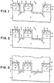
- the substrate 1 can be a P-type silicon substrate having any desired crystal orientation (e.g. ⁇ 100>):
- a P-type silicon substrate having any desired crystal orientation (e.g. ⁇ 100>):
- Such a substrate can be prepared by slicing and polishing a P-type silicon boule grown in the presence of a P-type dopant, such as boron, following conventional crystal growth techniques.
- P-type dopants for silicon include aluminium, gallium, and indium.
- Each of the deep trenches 2 has a substantially horizontal surface 3 and substantially vertical surfaces 4. Generally, the surfaces 4 are vertical or less than about 5° from the vertical.
- the trenches can be formed by the process disclosed in U.S.-A-4,256,514. Generally, the ratio of the depth of the trench to the width of the trench is between about 3.5 to 1 and 2.5 to 1. Of course, larger ratios such as about 4 to 1 are within the scope of the present invention. Typically, the depth of the trench is about 3.5 to 4 microns and the width is about 1 to 2.5 microns.
- n+ regions 5 Adjacent the lower portion of the trenches 2 are n+ regions 5 and adjacent the upper portion of the trenches are n regions 6. Such regions are desirably formed by ion implantation or thermal diffusion either before or after the formation of the trenches 2.
- layer 7 is also grown along the horizontal surface 3 of trench 2.
- the non-nucleating layer is a relatively thin layer about 0.2 nm to about 0.5 nm thick and typically about 0.3 nm thick.
- the non-nucleating layer can be provided by any well-known method, such as by thermal oxidation.
- the thickness of the non-nucleating layer on surface 3 need not be the same as the thickness of the non-nucleating layer on surfaces 4.
- the non-nucleating layer 7 is provided on at least one of the surfaces located along the longest axis of the trench. In the structure shown in figure 1, the longest axis is along the vertical walls 4 of the trench.
- a layer 8 of nucleating material is formed on at least one of the surfaces of the non-nucleating layer 7 as shown in figure 2.
- this layer is about 500 to about 3000 angstroms thick. It has been noted that if the nucleating layer is too thin, or less than about 500 angstroms, then back etching can occur during the filling technique which thereby causes void formation and decreased speed in the filling technique.
- the nucleating layer can be deposited by either atmospheric or a low pressure CVD technique to provide polycrystalline silicon. It is preferred that the relatively thin nucleating layer be deposited by low temperature techniques, using temperatures up to about 650°C.
- Figure 2 illustrates a preferred configuration wherein the nucleating layer 8 is present only on the horizontal surface 3 of the trench and on the horizontal surfaces of the non-nucleating layer on top of the silicon substrate.
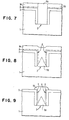
- figure 7 shows the nucleating layer 8 on top of the non-nucleating material 7 on the horizontal surface of the substrate located outside trench 2.
- the bottom 3 of trench 2 is exposed silicon which also acts as a nucleating material.
- Non-nucleating material 7 is present on the vertical walls of the trench.
- Figure 8 illustrates covering the non-nucleating material 7 on the vertical walls 4 of the trench and the horizontal layer outside the trench with a nucleating layer.
- the horizontal surface 3 of trench 2 is exposed substrate 1.
- Figure 9 illustrates providing nucleating material 8 on the non-nucleating material 7 on the vertical sidewalls 4 of trench 2.
- the horizontal bottom portion 3 of trench 2 is exposed silicon.
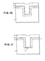
- Figure 10 illustrates providing a nucleating layer 8 on all surfaces above non-nucleating material 7.
- Figure 11 illustrates providing a nucleating layer 8 over all of the surfaces of trench 2 wherein the horizontal surface 3 of trench 2 is exposed silicon substrate and the vertical surfaces 4 of trench 2 are non-nucleating material 7.
- the techniques illustrated in figures 8-11 are not particularly preferred since small amounts of voids have been noted in their formation.
- the nucleating material within the trench be present on either only the vertical surfaces 4 or only on the horizontal surface 3.
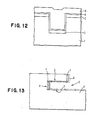
- Figure 12 illustrates providing a non-nucleating material layer 7 on the horizontal surface of trench 2 and on the horizontal surfaces located outside trench 2.
- the nucleating layer 8 is provided over all surfaces of the trench (ie vertical walls 4, horizontal surface 3) and on the horizontal surface above the non-nucleating layer 7 on the substrate located outside trench 2.
- the present invention is also applicable to filling trenches which are located substantially parallel to or at any angle to the top surface of the substrate in addition to the trenches shown which are substantially perpendicular to the top surface of the substrate.
- figure 13 illustrates a structure wherein the trench is about 90° from that shown in figure 12.
- figure 13 illustrates providing a non-nucleating material layer 7 on the vertical surface of the trench 2.
- the nucleating layer 8 is provided over all surfaces of the trench and on the vertical surfaces outside the trench.
- the preferred nucleating layer is polycrystalline silicon.
- silicon 9 is grown in trench 2 and on all surfaces containing the nucleating material.
- the preferred method of growing the silicon according to the present invention is by a gas-solid or heterogeneous reaction system.
- the growth occurs perpendicularly from the nucleated surfaces.
- the heterogeneous reaction system desirably includes hydrogen, silicon, and chlorine.
- a particularly preferred system is a combination of SiCl 4-H2as discussed by Silvestri and Tang - Reproducible Technique for Simultaneous Deposition of Poly-Epi on Oxide-Silicon, IBM Technical Disclosure Bulletin, Volume 23, No 2, July 1980, pages 819 and 820.
- the filling process is generally carried out at temperatures between about 900 and about 1100°C and preferably about 1000°C to provide a sufficiently fast filling of the trenches. It is important that the filling of the trenches is completed in about 20 minutes or less so that the dopant impurities already present in the substrate are not disturbed due to the exposure to elevated temperatures. With the typical dimensions discussed hereinabove, the filling rate to provide a practical process is at least about 0.22 microns per minute.
- silicon fill that will be present within the trenches will depend upon the type of nucleating surface present. For instance, polycrystalline nucleating surfaces will result in the formation of polycrystalline silicon. On the other hand, silicon nucleating surfaces, such as shown in figures 7, 8, and 9 will result in epitaxial silicon growth. Accordingly, as illustrated in figures 7, 8, and 9 there will be a combination of polycrystalline silicon 9A and epitaxial silicon 9B.
- the silicon layer 9 is planarized for example by a technique discussed in U.S.-A-4,256,514 employing either Cl/argon or CBrF 3 .
- the preferred technique comprises providing a relatively thick layer of resist material 10 over the grown silicon surfaces as illustrated in figure 4.
- the photoresist material can be applied by well-known techniques such as spinning on or by spraying.
- the photoresist material tends to flow and provide a substantially level surface as indicated in figure 4.
- the particular photoresist material employed for this purpose is not critical and any type, negative or positive, of photoresist material can be employed. This is possible since the subsequent steps, as will be discussed hereinbelow, are not dependent upon the chemical identity of the photoresist material.
- Suitable photoresist materials include compositions based on phenol formaldehyde novalak polymers.
- a particular example of such is Shipley 1350 which is an m-cresol formaldehyde novalak polymer composition.
- This is a positive resist composition and includes therein a diazoketone, such as 2-diazo-1-naphthol-5-sulphonic acid ester.
- the composition usually contains about 15% by weight of the diazoketone compound.
- the diazoketone is attached directly to the polymer molecules.
- photoresist materials can be found, for instance, in Journal of the Electrochemical Society, Vol 125, No 3, March 1980 - Deckert et al, "Micro-lithography - Key to Solid-State Fabrication", pp 45C to 56C.
- the photoresist is generally applied in a thickness of about 2 to about 4 microns.
- the reactive ion etching procedure employs conditions such that polycrystalline silicon and/or epitaxial silicon etches at the same rate as the photoresist material and at a rate substantially higher than silicon dioxide.
- the relative amount of the reactive gases, in particular CF4 and 0 2 , and the pressure and the rf power to the two electrodes are adjusted such that the etch rate of the photoresist material is about equal to that of the epitaxial silicon.
- a particularly preferred system contains about 20% by volume of 0 at a pressure of about 100 millitorr (13.3 N/m 2 ).
- the rf power density to the substrate electrode is 0.27W/cm 2 and the rf power density to the substrate electrode is 0.1W/cm 2 .
- the flow rate of the etching gas is about 40 SCCM and the temperature of the wafer is between 60 and 100°C. Under these conditions, the etch rate of silicon and photoresist is about 60nm/min and the etch rate of SiO is 7.0 nm/min. Thus, etching stops at the oxide surface 7.
- the silicon is etched a small distance inside the trench 2, such as about 200 nm.
- the particular devices can be fabricated on and in the substrate.
- the surfaces of the remaining polycrystalline silicon 9 in the trench can be doped to provide an n+ region, for example by being doped with POC1 3 .
- the polycrystalline silicon can now be oxidized to provide isolation regions 11 on top of the n+ regions. It is noted that the polycrystalline silicon, since it is heavily doped, is oxidized about 4 times as fast as oxidation growth on the epitaxial silicon at a temperature of about 800°C. Accordingly, subsequent to the oxide growth, the oxide can be etched to leave oxide remaining on the polycrystalline silicon, but exposing the epitaxial silicon region.
Landscapes
- Element Separation (AREA)
Applications Claiming Priority (2)
| Application Number | Priority Date | Filing Date | Title |
|---|---|---|---|
| US393997 | 1982-06-30 | ||
| US06/393,997 US4473598A (en) | 1982-06-30 | 1982-06-30 | Method of filling trenches with silicon and structures |
Publications (3)
| Publication Number | Publication Date |
|---|---|
| EP0097789A2 true EP0097789A2 (de) | 1984-01-11 |
| EP0097789A3 EP0097789A3 (en) | 1986-08-20 |
| EP0097789B1 EP0097789B1 (de) | 1990-04-11 |
Family
ID=23557108
Family Applications (1)
| Application Number | Title | Priority Date | Filing Date |
|---|---|---|---|
| EP83104287A Expired EP0097789B1 (de) | 1982-06-30 | 1983-05-02 | Verfahren zum Füllen mit Silizium von Gräben in Halbleitersubstraten |
Country Status (4)
| Country | Link |
|---|---|
| US (1) | US4473598A (de) |
| EP (1) | EP0097789B1 (de) |
| JP (1) | JPS598351A (de) |
| DE (1) | DE3381459D1 (de) |
Cited By (8)
| Publication number | Priority date | Publication date | Assignee | Title |
|---|---|---|---|---|
| FR2595507A1 (fr) * | 1986-03-07 | 1987-09-11 | Canon Kk | Procede de fabrication d'un element de memoire a semi-conducteurs |
| EP0107902B1 (de) * | 1982-09-29 | 1989-04-19 | Fujitsu Limited | Verfahren zur Herstellung von Isolationszonen in Halbleiteranordnungen |
| EP0166140A3 (en) * | 1984-06-25 | 1989-06-14 | International Business Machines Corporation | Integrated circuit isolation structure and method of making |
| EP0200771B1 (de) * | 1984-11-01 | 1989-07-26 | Ncr Corporation | Verfahren zur herstellung von isolationszonen in einem halbleitersubstrat |
| EP0338480A1 (de) * | 1988-04-18 | 1989-10-25 | Motorola, Inc. | Verfahren zur Grabenfüllung mittels einer Keimschicht |
| EP0226739B1 (de) * | 1985-12-20 | 1990-12-19 | Licentia Patent-Verwaltungs-GmbH | Strukturierte Halbleiterkörper |
| EP0495974A4 (en) * | 1990-08-06 | 1993-06-23 | Harris Corporation | Trench conductors and crossover architecture |
| US5342792A (en) * | 1986-03-07 | 1994-08-30 | Canon Kabushiki Kaisha | Method of manufacturing semiconductor memory element |
Families Citing this family (60)
| Publication number | Priority date | Publication date | Assignee | Title |
|---|---|---|---|---|
| GB2104722B (en) * | 1981-06-25 | 1985-04-24 | Suwa Seikosha Kk | Mos semiconductor device and method of manufacturing the same |
| USRE34400E (en) * | 1982-09-29 | 1993-10-05 | Fujitsu Limited | Method for fabricating isolation region in semiconductor devices |
| JPS6039846A (ja) * | 1983-08-15 | 1985-03-01 | Oki Electric Ind Co Ltd | 半導体集積回路装置の製造方法 |
| JPS6054453A (ja) * | 1983-09-05 | 1985-03-28 | Oki Electric Ind Co Ltd | 半導体集積回路装置の製造方法 |
| US4680614A (en) * | 1984-06-25 | 1987-07-14 | Beyer Klaus D | Planar void free isolation structure |
| US4526631A (en) * | 1984-06-25 | 1985-07-02 | International Business Machines Corporation | Method for forming a void free isolation pattern utilizing etch and refill techniques |
| US4689656A (en) * | 1984-06-25 | 1987-08-25 | International Business Machines Corporation | Method for forming a void free isolation pattern and resulting structure |
| US4589193A (en) * | 1984-06-29 | 1986-05-20 | International Business Machines Corporation | Metal silicide channel stoppers for integrated circuits and method for making the same |
| JPS6276645A (ja) * | 1985-09-30 | 1987-04-08 | Toshiba Corp | 複合半導体結晶体構造 |
| US4745081A (en) * | 1985-10-31 | 1988-05-17 | International Business Machines Corporation | Method of trench filling |
| JP2566914B2 (ja) * | 1985-12-28 | 1996-12-25 | キヤノン株式会社 | 薄膜半導体素子及びその形成法 |
| US4789560A (en) * | 1986-01-08 | 1988-12-06 | Advanced Micro Devices, Inc. | Diffusion stop method for forming silicon oxide during the fabrication of IC devices |
| US4671970A (en) * | 1986-02-05 | 1987-06-09 | Ncr Corporation | Trench filling and planarization process |
| US4666737A (en) * | 1986-02-11 | 1987-05-19 | Harris Corporation | Via metallization using metal fillets |
| JPH0782996B2 (ja) * | 1986-03-28 | 1995-09-06 | キヤノン株式会社 | 結晶の形成方法 |
| JP2662396B2 (ja) * | 1986-03-31 | 1997-10-08 | キヤノン株式会社 | 結晶性堆積膜の形成方法 |
| US5084413A (en) * | 1986-04-15 | 1992-01-28 | Matsushita Electric Industrial Co., Ltd. | Method for filling contact hole |
| JPS63122261A (ja) * | 1986-11-12 | 1988-05-26 | Mitsubishi Electric Corp | 半導体装置の製造方法 |
| US4906585A (en) * | 1987-08-04 | 1990-03-06 | Siemens Aktiengesellschaft | Method for manufacturing wells for CMOS transistor circuits separated by insulating trenches |
| US5298450A (en) * | 1987-12-10 | 1994-03-29 | Texas Instruments Incorporated | Process for simultaneously fabricating isolation structures for bipolar and CMOS circuits |
| US4876214A (en) * | 1988-06-02 | 1989-10-24 | Tektronix, Inc. | Method for fabricating an isolation region in a semiconductor substrate |
| US4853344A (en) * | 1988-08-12 | 1989-08-01 | Advanced Micro Devices, Inc. | Method of integrated circuit isolation oxidizing walls of isolation slot, growing expitaxial layer over isolation slot, and oxidizing epitaxial layer over isolation slot |
| US5008208A (en) * | 1988-12-07 | 1991-04-16 | Honeywell Inc. | Method of making planarized, self-aligned bipolar integrated circuits |
| JPH0736424B2 (ja) * | 1988-12-17 | 1995-04-19 | 日本電気株式会社 | 読み出し専用半導体記憶装置の製造方法 |
| US4963506A (en) * | 1989-04-24 | 1990-10-16 | Motorola Inc. | Selective deposition of amorphous and polycrystalline silicon |
| US5332683A (en) * | 1989-06-14 | 1994-07-26 | Kabushiki Kaisha Toshiba | Method of manufacturing semiconductor device having elements isolated by trench |
| US5234861A (en) * | 1989-06-30 | 1993-08-10 | Honeywell Inc. | Method for forming variable width isolation structures |
| US5017999A (en) * | 1989-06-30 | 1991-05-21 | Honeywell Inc. | Method for forming variable width isolation structures |
| US4942137A (en) * | 1989-08-14 | 1990-07-17 | Motorola, Inc. | Self-aligned trench with selective trench fill |
| US5049521A (en) * | 1989-11-30 | 1991-09-17 | Silicon General, Inc. | Method for forming dielectrically isolated semiconductor devices with contact to the wafer substrate |
| US4992388A (en) * | 1989-12-10 | 1991-02-12 | Motorola, Inc. | Short channel IGFET process |
| US5077228A (en) * | 1989-12-01 | 1991-12-31 | Texas Instruments Incorporated | Process for simultaneous formation of trench contact and vertical transistor gate and structure |
| JPH07105497B2 (ja) * | 1990-01-31 | 1995-11-13 | 新技術事業団 | 半導体デバイス及びその製造方法 |
| US5413966A (en) * | 1990-12-20 | 1995-05-09 | Lsi Logic Corporation | Shallow trench etch |
| US5290396A (en) * | 1991-06-06 | 1994-03-01 | Lsi Logic Corporation | Trench planarization techniques |
| US5248625A (en) * | 1991-06-06 | 1993-09-28 | Lsi Logic Corporation | Techniques for forming isolation structures |
| JPH0513566A (ja) * | 1991-07-01 | 1993-01-22 | Toshiba Corp | 半導体装置の製造方法 |
| JP2549884Y2 (ja) * | 1991-08-21 | 1997-10-08 | 三菱重工業株式会社 | シール機械 |
| DE4300986C2 (de) * | 1992-01-17 | 1999-08-26 | Mitsubishi Electric Corp | Halbleitervorrichtung zur Elementisolierung und Herstellungsverfahren derselben |
| US5213989A (en) * | 1992-06-24 | 1993-05-25 | Motorola, Inc. | Method for forming a grown bipolar electrode contact using a sidewall seed |
| US5387538A (en) * | 1992-09-08 | 1995-02-07 | Texas Instruments, Incorporated | Method of fabrication of integrated circuit isolation structure |
| US5457068A (en) * | 1992-11-30 | 1995-10-10 | Texas Instruments Incorporated | Monolithic integration of microwave silicon devices and low loss transmission lines |
| US5354706A (en) * | 1993-03-02 | 1994-10-11 | Lsi Logic Corporation | Formation of uniform dimension conductive lines on a semiconductor wafer |
| JP2526786B2 (ja) * | 1993-05-22 | 1996-08-21 | 日本電気株式会社 | 半導体装置及びその製造方法 |
| EP0631306B1 (de) * | 1993-06-23 | 2000-04-26 | Siemens Aktiengesellschaft | Verfahren zur Herstellung von einem Isolationsgraben in einem Substrat für Smart-Power-Technologien |
| US5346584A (en) * | 1993-07-28 | 1994-09-13 | Digital Equipment Corporation | Planarization process for IC trench isolation using oxidized polysilicon filler |
| US5994718A (en) * | 1994-04-15 | 1999-11-30 | National Semiconductor Corporation | Trench refill with selective polycrystalline materials |
| DE29606526U1 (de) * | 1996-04-10 | 1996-08-14 | Trw Occupant Restraint Systems Gmbh, 73551 Alfdorf | Gurthöhenversteller für ein Fahrzeug-Sicherheitsgurtsystem |
| US5889293A (en) * | 1997-04-04 | 1999-03-30 | International Business Machines Corporation | Electrical contact to buried SOI structures |
| DE69940422D1 (de) * | 1999-04-30 | 2009-04-02 | St Microelectronics Srl | Herstellungsverfahren für integrierte SOI Schaltkreisstrukturen |
| GB2369453B (en) * | 2000-11-24 | 2002-07-31 | Bookham Technology Plc | Fabrication of integrated circuit |
| KR100421046B1 (ko) * | 2001-07-13 | 2004-03-04 | 삼성전자주식회사 | 반도체 장치 및 그 제조방법 |
| US6902867B2 (en) * | 2002-10-02 | 2005-06-07 | Lexmark International, Inc. | Ink jet printheads and methods therefor |
| US6888214B2 (en) * | 2002-11-12 | 2005-05-03 | Micron Technology, Inc. | Isolation techniques for reducing dark current in CMOS image sensors |
| US7109097B2 (en) * | 2004-12-14 | 2006-09-19 | Applied Materials, Inc. | Process sequence for doped silicon fill of deep trenches |
| FR2907916B1 (fr) * | 2006-10-31 | 2009-01-23 | Commissariat Energie Atomique | Nouvelle structure de guide a fente |
| FR2907917B1 (fr) * | 2006-10-31 | 2009-01-23 | Commissariat Energie Atomique | Nouvelle structure de guide a fente |
| CN105185737A (zh) * | 2014-05-30 | 2015-12-23 | 无锡华润上华半导体有限公司 | 沟槽隔离结构的制造方法 |
| US9852902B2 (en) * | 2014-10-03 | 2017-12-26 | Applied Materials, Inc. | Material deposition for high aspect ratio structures |
| CN109148276A (zh) * | 2018-08-20 | 2019-01-04 | 上海华虹宏力半导体制造有限公司 | 提高深沟槽填充能力的方法 |
Family Cites Families (12)
| Publication number | Priority date | Publication date | Assignee | Title |
|---|---|---|---|---|
| US3425879A (en) * | 1965-10-24 | 1969-02-04 | Texas Instruments Inc | Method of making shaped epitaxial deposits |
| US3979237A (en) * | 1972-04-24 | 1976-09-07 | Harris Corporation | Device isolation in integrated circuits |
| US3969168A (en) * | 1974-02-28 | 1976-07-13 | Motorola, Inc. | Method for filling grooves and moats used on semiconductor devices |
| US3998673A (en) * | 1974-08-16 | 1976-12-21 | Pel Chow | Method for forming electrically-isolated regions in integrated circuits utilizing selective epitaxial growth |
| JPS54590A (en) * | 1977-06-03 | 1979-01-05 | Hitachi Ltd | Element isolating method |
| JPS5432984A (en) * | 1977-08-19 | 1979-03-10 | Hitachi Ltd | Integrated circuit device |
| US4256514A (en) * | 1978-11-03 | 1981-03-17 | International Business Machines Corporation | Method for forming a narrow dimensioned region on a body |
| US4191788A (en) * | 1978-11-13 | 1980-03-04 | Trw Inc. | Method to reduce breakage of V-grooved <100> silicon substrate |
| US4255207A (en) * | 1979-04-09 | 1981-03-10 | Harris Corporation | Fabrication of isolated regions for use in self-aligning device process utilizing selective oxidation |
| DE3072040D1 (en) * | 1979-07-23 | 1987-11-05 | Fujitsu Ltd | Method of manufacturing a semiconductor device wherein first and second layers are formed |
| DE3129558A1 (de) * | 1980-07-28 | 1982-03-18 | Tokyo Shibaura Denki K.K., Kawasaki, Kanagawa | Verfahren zur herstellung einer integrierten halbleiterschaltung |
| JPS58154256A (ja) * | 1982-03-10 | 1983-09-13 | Hitachi Ltd | 半導体装置 |
-
1982
- 1982-06-30 US US06/393,997 patent/US4473598A/en not_active Expired - Lifetime
-
1983
- 1983-04-20 JP JP58068500A patent/JPS598351A/ja active Pending
- 1983-05-02 EP EP83104287A patent/EP0097789B1/de not_active Expired
- 1983-05-02 DE DE8383104287T patent/DE3381459D1/de not_active Expired - Lifetime
Cited By (8)
| Publication number | Priority date | Publication date | Assignee | Title |
|---|---|---|---|---|
| EP0107902B1 (de) * | 1982-09-29 | 1989-04-19 | Fujitsu Limited | Verfahren zur Herstellung von Isolationszonen in Halbleiteranordnungen |
| EP0166140A3 (en) * | 1984-06-25 | 1989-06-14 | International Business Machines Corporation | Integrated circuit isolation structure and method of making |
| EP0200771B1 (de) * | 1984-11-01 | 1989-07-26 | Ncr Corporation | Verfahren zur herstellung von isolationszonen in einem halbleitersubstrat |
| EP0226739B1 (de) * | 1985-12-20 | 1990-12-19 | Licentia Patent-Verwaltungs-GmbH | Strukturierte Halbleiterkörper |
| FR2595507A1 (fr) * | 1986-03-07 | 1987-09-11 | Canon Kk | Procede de fabrication d'un element de memoire a semi-conducteurs |
| US5342792A (en) * | 1986-03-07 | 1994-08-30 | Canon Kabushiki Kaisha | Method of manufacturing semiconductor memory element |
| EP0338480A1 (de) * | 1988-04-18 | 1989-10-25 | Motorola, Inc. | Verfahren zur Grabenfüllung mittels einer Keimschicht |
| EP0495974A4 (en) * | 1990-08-06 | 1993-06-23 | Harris Corporation | Trench conductors and crossover architecture |
Also Published As
| Publication number | Publication date |
|---|---|
| EP0097789B1 (de) | 1990-04-11 |
| US4473598A (en) | 1984-09-25 |
| EP0097789A3 (en) | 1986-08-20 |
| DE3381459D1 (de) | 1990-05-17 |
| JPS598351A (ja) | 1984-01-17 |
Similar Documents
| Publication | Publication Date | Title |
|---|---|---|
| EP0097789B1 (de) | Verfahren zum Füllen mit Silizium von Gräben in Halbleitersubstraten | |
| US4758531A (en) | Method of making defect free silicon islands using SEG | |
| US4528047A (en) | Method for forming a void free isolation structure utilizing etch and refill techniques | |
| US4526631A (en) | Method for forming a void free isolation pattern utilizing etch and refill techniques | |
| EP0036111B1 (de) | Verfahren zur Herstellung einer feinen, tiefen dielektrischen Isolation | |
| US5308785A (en) | Isolation technique for silicon germanium devices | |
| US4771328A (en) | Semiconductor device and process | |
| US4519128A (en) | Method of making a trench isolated device | |
| US4307180A (en) | Process of forming recessed dielectric regions in a monocrystalline silicon substrate | |
| US6051511A (en) | Method and apparatus for reducing isolation stress in integrated circuits | |
| US4104086A (en) | Method for forming isolated regions of silicon utilizing reactive ion etching | |
| US5192708A (en) | Sub-layer contact technique using in situ doped amorphous silicon and solid phase recrystallization | |
| EP0107902B1 (de) | Verfahren zur Herstellung von Isolationszonen in Halbleiteranordnungen | |
| US4729006A (en) | Sidewall spacers for CMOS circuit stress relief/isolation and method for making | |
| US4056413A (en) | Etching method for flattening a silicon substrate utilizing an anisotropic alkali etchant | |
| US4619033A (en) | Fabricating of a CMOS FET with reduced latchup susceptibility | |
| US4900689A (en) | Method of fabrication of isolated islands for complementary bipolar devices | |
| EP0405923B1 (de) | Verfahren zur Herstellung von Isolationsstrukturen mit variabler Breite | |
| US5234861A (en) | Method for forming variable width isolation structures | |
| EP0068275A2 (de) | Verfahren zur Herstellung von Halbleiteranordnungen mittels reaktiven Ionenätzens | |
| EP0190581B1 (de) | Senkrecht isolierte komplementäre Transistorstrukturen | |
| US4680614A (en) | Planar void free isolation structure | |
| US5273934A (en) | Method for producing a doped region in a substrate | |
| EP0214512A2 (de) | Epitaxial hergestellte Anordnung mit Isolationszonen | |
| EP0137195B1 (de) | Dielektrisch isolierte Schaltung und Verfahren zur Herstellung |
Legal Events
| Date | Code | Title | Description |
|---|---|---|---|
| PUAI | Public reference made under article 153(3) epc to a published international application that has entered the european phase |
Free format text: ORIGINAL CODE: 0009012 |
|
| AK | Designated contracting states |
Designated state(s): DE FR GB |
|
| 17P | Request for examination filed |
Effective date: 19840426 |
|
| PUAL | Search report despatched |
Free format text: ORIGINAL CODE: 0009013 |
|
| AK | Designated contracting states |
Kind code of ref document: A3 Designated state(s): DE FR GB |
|
| 17Q | First examination report despatched |
Effective date: 19881003 |
|
| GRAA | (expected) grant |
Free format text: ORIGINAL CODE: 0009210 |
|
| AK | Designated contracting states |
Kind code of ref document: B1 Designated state(s): DE FR GB |
|
| REF | Corresponds to: |
Ref document number: 3381459 Country of ref document: DE Date of ref document: 19900517 |
|
| ET | Fr: translation filed | ||
| PLBE | No opposition filed within time limit |
Free format text: ORIGINAL CODE: 0009261 |
|
| STAA | Information on the status of an ep patent application or granted ep patent |
Free format text: STATUS: NO OPPOSITION FILED WITHIN TIME LIMIT |
|
| 26N | No opposition filed | ||
| PGFP | Annual fee paid to national office [announced via postgrant information from national office to epo] |
Ref country code: GB Payment date: 19950413 Year of fee payment: 13 |
|
| PGFP | Annual fee paid to national office [announced via postgrant information from national office to epo] |
Ref country code: FR Payment date: 19950427 Year of fee payment: 13 |
|
| PGFP | Annual fee paid to national office [announced via postgrant information from national office to epo] |
Ref country code: DE Payment date: 19950524 Year of fee payment: 13 |
|
| PG25 | Lapsed in a contracting state [announced via postgrant information from national office to epo] |
Ref country code: GB Effective date: 19960502 |
|
| GBPC | Gb: european patent ceased through non-payment of renewal fee |
Effective date: 19960502 |
|
| PG25 | Lapsed in a contracting state [announced via postgrant information from national office to epo] |
Ref country code: FR Effective date: 19970131 |
|
| PG25 | Lapsed in a contracting state [announced via postgrant information from national office to epo] |
Ref country code: DE Effective date: 19970201 |
|
| REG | Reference to a national code |
Ref country code: FR Ref legal event code: ST |