EP0092711A1 - Elektronisches, vorzugsweise berührungslos arbeitendes Schaltgerät - Google Patents
Elektronisches, vorzugsweise berührungslos arbeitendes Schaltgerät Download PDFInfo
- Publication number
- EP0092711A1 EP0092711A1 EP83103394A EP83103394A EP0092711A1 EP 0092711 A1 EP0092711 A1 EP 0092711A1 EP 83103394 A EP83103394 A EP 83103394A EP 83103394 A EP83103394 A EP 83103394A EP 0092711 A1 EP0092711 A1 EP 0092711A1
- Authority
- EP
- European Patent Office
- Prior art keywords
- switching device
- exclusive
- gate
- input
- voltage source
- Prior art date
- Legal status (The legal status is an assumption and is not a legal conclusion. Google has not performed a legal analysis and makes no representation as to the accuracy of the status listed.)
- Granted
Links
Images


Classifications
-
- H—ELECTRICITY
- H03—ELECTRONIC CIRCUITRY
- H03K—PULSE TECHNIQUE
- H03K17/00—Electronic switching or gating, i.e. not by contact-making and –breaking
- H03K17/94—Electronic switching or gating, i.e. not by contact-making and –breaking characterised by the way in which the control signals are generated
- H03K17/945—Proximity switches
Definitions
- the invention relates to an electronic, preferably non-contact switching device with a presence indicator that can be influenced from the outside, for. B. an oscillator with an electronic switch controllable by the presence indicator, e.g. B. a thyristor, a transistor or a triac, and with an exclusive OR gate provided between the presence indicator and the control input of the electronic switch, the first input of the exclusive OR gate to the output of the presence indicator (or a switching amplifier connected downstream of the presence indicator ) is connected, a reverse control signal can be applied to the second input of the exclusive OR gate and the output of the exclusive OR gate is connected to the control input of the electronic switch and a first and a second switching device connection are provided.
- an oscillator with an electronic switch controllable by the presence indicator, e.g. B. a thyristor, a transistor or a triac, and with an exclusive OR gate provided between the presence indicator and the control input of the electronic switch, the first input of the exclusive OR gate to the output of the presence indicator (
- Electronic switching devices of the type described above are designed without contact and are increasingly being used in electrical measuring, control and regulating circuits instead of electrical, mechanically operated switching devices which are designed with contacts.
- proximity switches are used to indicate whether an influencing element for which the corresponding proximity switch is sensitive has approached the proximity switch sufficiently far. If an influencing element for which the corresponding proximity switch is sensitive has approached the presence indicator sufficiently far, the presence indicator reverses the electronic switch, i. H. in the case of a switching device designed as a make contact, the non-conductive electronic switch now becomes conductive, while in the case of a switching device designed as a break contact, the conductive electronic switch now blocks.
- Switchching devices of the type in question can also be used to indicate whether a physical quantity of an influencing medium for which the switching device is sensitive has reached a corresponding value.
- a. the presence indicator that can be influenced from outside.
- a presence indicator e.g. B. an inductively or capacitively controllable oscillator can be provided; they are then inductive or capacitive proximity switches (see, e.g., German Offenlegungsschriften or Auslegeschrippen or patent documents 19 51 137, 19 66 178, 19 66 213, 20 36 840, 21 27 956, 22 03 038, 22 03 039, 22 03 040, 22 03 906, 23 30 233, 23 31 732. 23 56 490, 26 13 423, 26 16 265, 26 16 733, 26 28 427, 27 11 877 and 27 44 7851.
- a photo resistor, a photodiode or a phototransistor can also be provided; these are then optoelectronic proximity switches (see, for example, German published patent application 28 24 582).
- K. V ⁇ 1 i.e. H. the oscillator is not oscillating.
- the electronic switch e.g. B. a transistor, a thyristor or a triac controlled.
- Optoelectronic proximity switches have a light transmitter and a light receiver and are also referred to as light barriers.
- a distinction is made between a type of light barrier in which the light transmitter and the light receiver are arranged on opposite sides of a monitoring path and a light barrier type in which the light transmitter and the light receiver are arranged at the same end of a monitoring path, while a reflector is arranged at the other end of the monitoring path reflects the light beam coming from the light transmitter back to the light receiver.
- the presence indicator responds when the light beam normally coming from the light transmitter to the light receiver is interrupted by an influencing element that has reached the monitoring path.
- German Offenlegungsschriften or interpretations or patent documents 19 51 137, 19 66 178, 19 66 213, 20 36 840, 21 27 956, 22 03 038, 22 03 039, 22 03 040, 22 03 906, 23 30 233 , 23 31 732, 23 56 490, 26 13 423, 26 16 265, 26 16 773, 26 28 427, 27 11 877, 27 44 785, 29 43 911, 30 04 829, 30 38 102, 30 38 141 and 30 38 692.
- the second input of the exclusive OR gate is connected via a current limiting resistor to the plus potential of an auxiliary voltage source representing the reversal control signal and can be connected to the minus potential of the auxiliary voltage source. If the second input of the exclusive OR gate is connected to the negative potential of the auxiliary voltage source, then a reverse control signal is not effective at the second input of the exclusive OR gate.
- the switching device in question is "programmable", for. B. namely as a closer or opener.
- electronic switching devices of the type in question which have a presence indicator with two non-equivalent outputs and two electronic switches (cf. DE-ASen 29 31 879 and 29 31 880).
- two switching devices namely a switching device designed as a make contact and a switching device designed as a break contact, are combined to form a double switching device, the two switching devices having a presence indicator in common.
- this double switching device is complex in that it requires two electronic switches - and then, if it is to be used for an operating voltage source carrying alternating voltage, also two rectifier bridges.
- the invention is based on the object, the electronic switching device known from DE-PS 26 28 427, from which the invention is based, in terms of its "programmability", that is, in relation to the implementation as a closer or an opener simplify.
- the electronic switching device in which the above-mentioned object is achieved, is initially and essentially characterized in that a third switching device connection is provided and at the second input of the exclusive OR gate when the first and the second switching device connection are connected to the operating voltage source are, the reverse control valve is present, and when the first and third switching device connections are connected to the operating voltage source, no reverse control signal is present (or vice versa).
- connection programming ie an automatic realization as a closer or as a break contact, namely in that the switching device according to the invention is connected as a make contact - connection using the first and second switching device connection - or is connected as a break contact - connection using the first and third switching device connection.
- the second input of the exclusive OR gate can also be used with the switching device according to the invention on the one hand - preferably via a current limiting resistor - to the positive potential of an auxiliary voltage source, which represents the reversal control signal. Then, according to the invention, the second input of the exclusive OR gate, on the other hand, can be connected to the negative potential of the auxiliary voltage source by connecting the first and third switching device connections to the operating voltage source.
- Electronic switching devices of the type in question exist as AC voltage devices, that is to say for operating voltage sources carrying an AC voltage, and as DC voltage devices, that is to say for operating voltage sources carrying DC voltage.
- AC voltage devices that is to say for operating voltage sources carrying an AC voltage
- DC voltage devices that is to say for operating voltage sources carrying DC voltage.
- teaching of the invention can be applied to both AC devices and DC devices.
- the teaching of the invention can be implemented specifically in that two further rectifier elements are provided on the input side are provided and are each connected on the one hand to two other rectifier elements and on the other hand to the third switching device connection and the second input of the exclusive OR gate is connected to the third switching device connection.
- the teaching of the invention can be implemented specifically in that the third switching device connection is connected to the second switching device connection via a rectifier element, the direction of passage of the rectifier element from second switching device connection goes to the third switching device connection.
- a diode can be used as a rectifier element.
- a Zener diode it is advisable to use a Zener diode as a rectifier element so that interference voltages remain without influence.
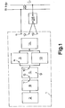
- the electronic switching device 1 shown in the figures works without contact and consists essentially of a presence indicator 2 which can be influenced from the outside, in the exemplary embodiment shown an oscillator, and an electronic switch 3 which can be controlled by the presence indicator 2, in the exemplary embodiment according to FIGS. 1 and 2 a thyristor 3, a transistor, and an exclusive OR gate 5 provided between the presence indicator 2 and the control input 4 of the electronic switch 3.
- the first input 6 of the exclusive OR gate 5 is at the output 7 of one of the Presence indicator 2 connected downstream switching amplifier 8, the second input 9 of the exclusive OR gate 5 can be acted upon with a reverse control signal and the output 10 of the exclusive OR gate 5 connected to the control input 4 of the electronic switch 3 and are a first and a second switching device connection 1 1, 12 provided.
- FIGS. 1 and 2 it is an AC voltage device.
- an auxiliary voltage source 13 is indicated here
- a rectifier bridge 14 with four rectifier elements 15, 16, 17, 18 is provided. 2 shows circuit details of the structure of an electronic switching device, which do not need to be explained here.
- a third switching device connection 19 is provided in the electronic switching device 1 in question and is at the second input 9 of the exclusive OR gate 5 when the first and second switching device connections 11, 12 are connected to the operating voltage source 20, the reverse control signal is present, while when the first and the third switching device connection 11, 19 are connected to the operating voltage source 20, no reverse control signal is present at the second input 9 of the exclusive OR gate 5 (or vice versa).
- the second input 9 of the exclusive OR gate 5 is connected on the one hand via a current limiting resistor 21 to the positive potential 21 of the auxiliary voltage source 13 which represents the reversal control signal and on the other hand in that the first and third switching device connections 11, 19 are connected to the operating voltage source 20 be connected to the negative potential 23 of the auxiliary voltage source 13.
- FIGS. 1 and 2 show an electronic switching device according to the invention in the embodiment as an AC voltage device.
- the teaching of the invention is realized in concrete terms in that two further rectifier elements 24, 25 are provided on the input side and are each connected on the one hand to two other rectifier elements 15, 17 or 16, 18 and on the other hand to the third switching device connection 19 and the second input 9 of the exclusive one OR gate 5 is connected to the third switching device connection 19, specifically via a decoupling diode 26.
- the embodiment of an electronic switching device according to the invention which is only indicated in FIG. 3 is a DC voltage device.
- the teaching of the invention is implemented in concrete terms in that the third switching device connection 19 is connected to the second switching device connection 12 via a rectifier element 27, in the exemplary embodiment a zener diode, the direction of passage of the rectifier element 27 going from the second switching device connection 12 to the third switching device connection 19.
- the switching device 1 is effective as a make contact when the second input 9 of the exclusive OR gate 5 is on Reverse control signal is present. It stands against second input 9 of the exclusive OR gate 5 no reversal control signal, the switching device 1 has the function of an opener. (Here, with regard to the exclusive OR gate 5, reference is again made to DE-PS 26 28 427, specifically to the truth table in column 2.)
- the switching device 1 according to the invention shown in FIGS. 1 and 2 as an AC voltage device is now connected to the operating voltage source 20 with the first switching device connection 11 - directly - and with the second switching device connection 12 - via a consumer 28 shown in FIG. 1, the third one hangs Switchgear connection 19 "in the air", so at the second input 9 of the exclusive OR gate 5 - via the current limiting resistor 21 - the positive potential 22 of the auxiliary voltage source 13, which represents the reverse control signal, is present.
- the switching device 1 thus works as a make contact when it is or is connected to the operating voltage source 20 via the first and the second switching device connection 11, 12.
- the switching device 1 thus works as a break contact when it is or is connected to the operating voltage source 20 via the first and the third switching device connection 11, 19.
- the switching device 1 also works here as a make contact if it is or is connected via the first and the second switching device connection 11, 12 to the operating voltage source, not shown here.
- the switching device 1 only indicated in FIG. 3 with the first switching device connection 11 - directly - and with the third switching device connection 19 - via a consumer (not shown here) - is connected to the operating voltage source (not shown), then the second input 9 of the exclusive OR -Gatters 5 practically connected to the negative potential 23 of the auxiliary voltage source, not shown, namely to a discharge potential which is below the negative potential 23 of the auxiliary voltage source, not shown, by the voltage drop across the zener diode 27, so that none at the second input 9 of the exclusive OR gate 5 Reverse control signal more pending.
- the switching device 1 thus works as a break contact when it is or is connected via the first and the third switching device connection 11, 19 to the operating voltage source, not shown in FIG. 3.
Landscapes
- Electronic Switches (AREA)
- Power Conversion In General (AREA)
- Switch Cases, Indication, And Locking (AREA)
Abstract
Description
- Die Erfindung betrifft ein elektronisches, vorzugsweise berührungslos arbeitendes Schaltgerät, mit einem von außen beeinflußbaren Anwesenheitsindikator, z. B. einem Oszillator, mit einem von dem Anwesenheitsindikator steuerbaren elektronischen Schalter, z. B. einem Thyristor, einem Transistor oder einem Triac, und mit einem zwischen dem Anwesenheitsindikator und dem Steuereingang des elektronischen Schalters vorgesehenen exklusiven ODER-Gatter, wobei der erste Eingang des exklusiven ODER-Gatters an den Ausgang des Anwesenheitsindikators (oder eines dem Anwesenheitsindikator nachgeschalteten Schaltverstärkers) angeschlossen ist, der zweite Eingang des exklusiven ODER-Gatters mit einem Umkehrsteuersignal beaufschlagbar ist und der Ausgang des exklusiven ODER-Gatters an den Steuereingang des elektronischen Schalters angeschlossen ist und wobei ein erster und ein zweiter Schaltgeräteanschluß vorgesehen sind.
- Elektronische Schaltgeräte der zuvor beschriebenen Art sind kontaktlos ausgeführt und werden in zunehmendem Maße anstelle von elektrischen, mechanisch betätigten Schaltgeräten, die kontaktbehaftet ausgeführt sind, in elektrischen Meß-, Steuer- und Regelkreisen verwendet. Das gilt insbesondere für sogenannte Annäherungsschalter, d. h. für elektronische Schaltgeräte, die berührungslos arbeiten. Mit solchen Annäherungsschaltern wird indiziert, ob sich ein Beeinflussungselement, für das der entsprechende Annäherungsschalter sensitiv ist, dem Annäherungsschalter hinreichend weit genähert hat. Hat sich nämlich ein Beeinflussungselement, für das der entsprechende Annäherungsschalter sensitiv ist, dem Anwesenheitsindikator hinreichend weit genähert, so steuert der Anwesenheitsindikator den elektronischen Schalter um, d. h. bei einem als Schließer ausgeführten Schaltgerät wird der nichtleitende elektronische Schalter nunmehr leitend, während bei einem als Öffner ausgeführten Schaltgerät der leitende elektronische Schalter nunmehr sperrt. (Mit Schaltgeräten der in Rede stehenden Art kann auch indiziert werden, ob eine physikalische Größe eines Beeinflussungsmediums, für die das Schaltgerät sensitiv ist, einen entsprechenden Wert erreicht hat.)
- Wesentlicher Bestandteil von elektronischen Schaltgeräten der zuvor beschriebenen Art ist also u. a. der von außen beeinflußbare Anwesenheitsindikator. Als Anwesenheitsindikator kann z. B. ein induktiv oder kapazitiv beeinflußbarer Oszillator vorgesehen sein; es handelt sich dann um induktive oder kapazitive Annäherungsschalter (vgl. z. B. die deutschen Offenlegungsschriften bzw. Auslegeschriften bzw. Patentschriften 19 51 137, 19 66 178, 19 66 213, 20 36 840, 21 27 956, 22 03 038, 22 03 039, 22 03 040, 22 03 906, 23 30 233, 23 31 732. 23 56 490, 26 13 423, 26 16 265, 26 16 733, 26 28 427, 27 11 877 und 27 44 7851. Als Anwesenheitsindikator kann z. B. auch ein Fotowiderstand, eine Fotodiode oder ein Fototransistor vorgesehen sein; es handelt sich dann um optoelektronische Annäherungsschalter (vgl. z. B. die deutsche Offenlegungsschrift 28 24 582).
- Bei induktiven Annäherungsschaltern gilt für den Oszillator, solange ein Metallteil einen vorgegebenen Abstand noch nicht erreicht hat, K- V = 1 mit K = Rückkopplungsfaktor und V = Verstärkungsfaktor des Oszillators, d. h. der Oszillator schwingt. Erreicht das entsprechende Metallteil den vorgeschriebenen Abstand, so führt die zunehmende Bedämpfung des Oszillators zu einer Verringerung des Verstärkungsfaktors V, so daß K . V < 1 wird, d. h. der Oszillator hört auf zu schwingen. Bei kapazitiven Annäherungsschaltern gilt für den Oszillator, solange ein Ansprechkörper die Kapazität zwischen einer Ansprechelektrode und einer Gegenelektrode noch nicht hinreichend vergrößert hat, also einen vorgegebenen Abstand noch nicht erreicht hat, K . V < 1, d. h. der Oszillator schwingt nicht. Erreicht der Ansprechkörper den vorgegebenen Abstand, so führt die steigende Kapazität zwischen der Ansprechelektrode und der Gegenelektrode zu einer Vergrößerung des Rückkopplungsfaktors K, so daß K V = 1 wird, d. h. der Oszillator beginnt zu schwingen. Bei beiden Ausführungsformen wird abhängig von den unterschiedlichen Zuständen des Oszillators der elektronische Schalter, z. B. ein Transistor, ein Thyristor oder ein Triac, gesteuert.
- Optoelektronische Annäherungsschalter weisen einen Lichtsender und einen Lichtempfänger auf und werden auch als Lichtschranken bezeichnet. Dabei unterscheidet man zwischen einem Lichtschrankentyp, bei dem der Lichtsender und der Lichtempfänger auf entgegengesetzten Seiten einer Überwachungsstrecke angeordnet sind, und einem Lichtschrankentyp, bei dem der Lichtsender und der Lichtempfänger am gleichen Ende einer überwachungsstrecke angeordnet sind, während ein am anderen Ende der Überwachungsstrecke angeordneter Reflektor den vom Lichtsender ausgehenden Lichtstrahl zum Lichtempfänger zurückreflektiert. In beiden Fällen spricht der Anwesenheitsindikator an, wenn der normalerweise vom Lichtsender zum Lichtempfänger gelangende Lichtstrahl durch ein in die Überwachungsstrecke gelangtes Beeinflussungselement unterbrochen wird. Es gibt jedoch auch Lichtschranken des zuletzt beschriebenen Lichtschrankentyps, bei dem der vom Lichtsender kommende Lichtstrahl nur durch ein entsprechendes Beeinflussungselement zum Lichtempfänger zurückreflektiert wird.
- Elektronische, berührungslos arbeitende Schaltgeräte sind anfangs mit einer Reihe von Problemen behaftet gewesen, - gemessen an elektrischen, mechanisch betätigten Schaltgeräten.-, nämlich u..a. mit den Problemen "Erzeugung einer Speisespannung für den Oszillator", "Ausbildung des Oszillators", "Einschaltimpulsverhinderung", "Kurzschlußfestigkeit". Mit diesen Problemen und deren Lösungen (und mit anderen bei elektronischen, berührungslos arbeitenden Schaltgeräten relevanten Problemen und deren Lösungen) befassen sich z. B. die deutschen Offenlegungsschriften bzw. Auslegeschriften bzw. Patentschriften 19 51 137, 19 66 178, 19 66 213, 20 36 840, 21 27 956, 22 03 038, 22 03 039, 22 03 040, 22 03 906, 23 30 233, 23 31 732, 23 56 490, 26 13 423, 26 16 265, 26 16 773, 26 28 427, 27 11 877, 27 44 785, 29 43 911, 30 04 829, 30 38 102, 30 38 141 und 30 38 692.
- Wie bereits angedeutet, werden elektronische Schaltgeräte der in Rede stehenden Art, wie elektrische Schaltgeräte auch, als Schließer oder als Öffner benötigt und gebaut. Die Notwendigkeit, elektronische Schaltgeräte der in Rede stehenden Art sowohl als Schließer als auch als öffner bauen und lagemäßig bereithalten zu müssen, ist aufwendig, - was einer näheren Erläuterung nicht bedarf.
- Aus der DE-PS 26 28 427, deren Offenbarungsgehalt hiermit ausdrücklich auch hier zur Offenbarung gemacht wird, ist es bekannt, bei einem elektronischen Schaltgerät der in Rede stehenden Art, und zwar konkret bei einem Schaltgerät mit einem von außen beeinflußbaren Oszillator und einem von dem Oszillator steuerbaren Thyristor, zwischen dem Oszillator und der Zündelektrode des Thyristors ein exklusives ODER-Gatter zu schalten, derart, daß der erste Eingang des exklusiven ODER-Gatters an den Ausgang des Oszillators oder eines dem Oszillator nachgeschalteten Schaltverstärkers angeschlossen, der zweite Eingang des exklusiven ODER-Gatters mit einem Umkehrsteuersignal beaufschlagbar und der Ausgang des exklusiven ODER-Gatters an die Zündelektrode des Thyristors angeschlossen ist. Dadurch ist die Aufgabe gelöst, ein elektronisches Schaltgerät der in Rede stehenden Art anzugeben, das sowohl als Schließer als auch als öffner benutzt und durch eine einfache Maßnahme am fertigen Schaltgerät zu einem Öffner bzw. zu einem Schließer gemacht werden kann. Im einzelnen ist dabei vorgesehen, daß der zweite Eingang des exklusiven ODER-Gatters über einen Strombegrenzungswiderstand an das das Umkehrsteuersignal darstellende Pluspotential einer Hilfsspannungsquelle angeschlossen und mit dem Minuspotential der Hilfsspannungsquelle verbindbar ist. Ist der zweite Eingang des exklusiven ODER-Gatters mit dem Minuspotential der Hilfsspannungsquelle verbunden, so ist am zweiten Eingang des exklusiven ODER-Gatters ein Umkehrsteuersignal nicht wirksam. Wird jedoch die Verbindung des zweiten Eingang des exklusiven ODER-Gatters mit dem Minuspotential der Hilfsspannungsquelle unterbrochen, so wird am zweiten Eingang des exklusiven ODER-Gatters das Pluspotential der Hilfsspannungsquelle als Umkehrsteuersignal wirksam. Durch die Unterbrechung bzw. die Herstellung einer Verbindung ist also das in Rede stehende Schaltgerät "programmierbar", z. B. nämlich als Schließer oder als Öffner.
- Im übrigen sind elektronische Schaltgeräte der in Rede stehenden Art bekannt, die einen Anwesenheitsindikator mit zwei antivalenten Ausgängen und zwei elektronischen Schaltern aufweisen (vgl. die DE-ASen 29 31 879 und 29 31 880). Hier sind gleichsam zwei Schaltgeräte, nämlich ein als Schließer ausgeführtes Schaltgerät und ein als Öffner ausgeführtes Schaltgerät, zu einem Doppel-Schaltgerät vereinigt, - wobei beiden Schaltgeräten ein Anwesenheitsindikator gemeinsam ist. Dieses Doppel-Schaltgerät ist jedoch insoweit aufwendig, als es zwei elektronische Schalter - und dann, wenn es für eine Wechsel Spannung führende Betriebsspannungsquelle verwendbar sein soll, auch zwei Gleichrichterbrücken benötigt.
- Der Erfindung liegt nun die Aufgabe zugrunde, das aus der DE-PS 26 28 427 bekannte elektronische Schaltgerät, von dem die Erfindung ausgeht, in bezug auf seine "Programmierbarkeit", also in bezug auf die Realisierung als Schließer oder als Öffner, noch weiter zu vereinfachen.
- Das erfindungsgemäße elektronische Schaltgerät, bei dem die zuvor aufgezeigte Aufgabe gelöst ist, ist zunächst und im wesentlichen dadurch gekennzeichnet, daß ein dritter Schaltgeräteanschluß vorgesehen ist und am zweiten Eingang des exklusiven ODER-Gatters dann, wenn der erste und der zweite Schaltgeräteanschluß an die Betriebsspannungsquelle angeschlossen sind, das Umkehrsteuerventil ansteht, und dann, wenn der erste und der dritte Schaltgeräteanschluß an die Betriebsspannungsquelle angeschlossen sind, kein Umkehrsteuersignal ansteht (oder umgekehrt). Während also bei dem elektronischen Schaltgerät, von dem die Erfindung ausgeht, eine "Programmierbarkeit" gegeben ist, nämlich die zielgerichtete Realisierung als Schließer oder als Öffner durch Unterbrechung oder Herstellung einer Verbindung zwischen dem zweiten Eingang des exklusiven ODER-Gatters und dem Minuspotential einer Hilfsspannungsquelle, ist bei dem erfindungsgemäßen elektronischen Schaltgerät gleichsam eine "Anschlußprogranunierbarkeit" gegeben, d. h. eine automatische Realisierung als Schließer oder als Öffner, nämlich dadurch, daß das erfindungsgemäße Schaltgerät als Schließer angeschlossen wird - Anschluß mit Hilfe des ersten und des zweiten Schaltgeräteanschlusses - oder eben als Öffner angeschlossen wird - Anschluß mit Hilfe des ersten und des dritten Schaltgeräteanschlusses.
- Im einzelnen gibt es verschiedene Möglichkeiten, das erfindungsgemäße elektronische Schaltgerät auszugestalten und weiterzubilden, was im folgenden nur beispielhaft erläutert werden soll.
- wie bei dem elektronischen Schaltgerät, von dem die Erfindung ausgeht (vgl. die DE-PS 26 28 427, deren Offenbarungsgehalt hiermit ausdrücklich auch hier zur Offenbarung gemacht wird), kann auch bei dem erfindungsgemäßen Schaltgerät der zweite Eingang des exklusiven ODER-Gatters einerseits - vorzugsweise über einen Strombegrenzungswiderstand - an das das Umkehrsteuersignal darstellende Pluspotential einer Hilfsspannungsquelle angeschlossen sein. Dann ist erfindungsgemäß der zweite Eingang des exklusiven ODER-Gatters andererseits dadurch, daß der erste und der dritte Schaltgeräteanschluß an die Betriebsspannungsquelle angeschlossen werden, an das Minuspotential der Hilfsspannungsquelle anschließbar.
- Elektronische Schaltgeräte der in Rede stehenden Art gibt es als Wechselspannungsgeräte, also für eine Wechselspannung führende Betriebsspannungsquelle, und als Gleichspannungsgeräte, also für eine Gleichspannung führende Betriebsspannungsquelle. Selbstverständlich kann die Lehre der Erfindung sowohl bei Wechselspannungsgeräten als auch bei Gleichspannungsgeräten angewendet werden.
- Bei einem Wechselspannungsgerät, also einem elektronischen Schaltgerät der in Rede stehenden Art für eine Wechselspannung führende Betriebsspannungsquelle und mit einer eingangsseitig vorgesehenen Gleichrichterbrücke mit vier Gleichrichterelementen, kann die Lehre der Erfindung konkret dadurch realisiert sein, daß eingangsseitig zwei weitere Gleichrichterelemente vorgesehen und jeweils einerseits mit zwei anderen Gleichrichterelementen und andererseits mit dem dritten Schaltgeräteanschluß verbunden sind und der zweite Eingang des exklusiven ODER-Gatters mit dem dritten Schaltgeräteanschluß verbunden ist. Dabei empfiehlt es sich, den zweiten Eingang des exklusiven ODER-Gatters über eine Entkoppeldiode mit dem dritten Schaltgeräteanschluß zu verbinden, - wobei die Entkoppeldiode verhindert, daß das Pluspotential der Betriebsspannungsquelle, das wesentlich über dem Pluspotential der Hilfsspannungsquelle liegt, an den zweiten Eingang des exklusiven ODER-Gatters gelangen kann.
- Bei einem Gleichspannungsgerät, also einem elektronischen Schaltgerät der in Rede stehenden Art für eine Gleichspannung führende Betriebsspannungsquelle, kann die Lehre der Erfindung konkret dadurch realisiert sein, daß der dritte Schaltgeräteanschluß über ein Gleichrichterelement mit dem zweiten Schaltgeräteanschluß verbunden ist, - wobei die Durchlaßrichtung des Gleichrichterelementes vom zweiten Schaltgeräteanschluß zum dritten Schaltgeräteanschluß geht. Funktionsmäßig kann als Gleichrichterelement ohne weiteres eine Diode verwendet werden. Es empfiehlt sich jedoch, als Gleichrichterelement eine Zenerdiode zu verwenden, so daß Störspannungen ohne Einfluß bleiben.
- Im folgenden wird die Erfindung anhand einer lediglich Ausführungsbeispiele darstellenden Zeichnung nochmals erläutert; es zeigt
- Fig. 1 das Blockschaltbild eines erfindungsgemäßen elektronischen, berührungslos arbeitenden Schaltgerätes, und zwar eines wechselspannungsgerätes,
- Fig. 2 das Schaltbild des Schaltgerätes nach Fig. 1 und
- Fig. 3 einen Ausschnitt aus dem Schaltbild eines als Gleichspannungsgerät ausgeführten erfindungsgemäßen elektronischen, berührungslos arbeitenden Schaltgerätes.
- Das in den Figuren dargestellte elektronische Schaltgerät 1 arbeitet berührungslos und besteht im wesentlichen aus einem von außen beeinflußbaren Anwesenheitsindikator 2, im dargestellten Ausführungsbeispiel einem Oszillator, aus einem von dem Anwesenheitsindikator 2 steuerbaren elektronischen Schalter 3, im Ausführungsbeispiel nach den Fig. 1 und 2 einem Thyristor, im Ausführungsbeispiel nach Fig. 3 einem Transistor, und aus einem zwischen dem Anwesenheitsindikator 2 und dem Steuereingang 4 des elektronischen Schalters 3 vorgesehenen exklusiven ODER-Gatter 5. Dabei ist der erste Eingang 6 des exklusiven ODER-Gatters 5 an den Ausgang 7 eines dem Anwesenheitsindikator 2 nachgeschalteten Schaltverstärkers 8 angeschlossen, der zweite Eingang 9 des exklusiven ODER-Gatters 5 mit einem Umkehrsteuersignal beaufschlagbar und der Ausgang 10 des exklusiven ODER-Gatters 5 an den Steuereingang 4 des elektronischen Schalters 3 angeschlossen und sind ein erster und ein zweiter Schaltgeräteanschluß 11, 12 vorgesehen.
- Im Ausführungsbeispiel nach den Fig. 1 und 2 handelt es sich um ein Wechselspannungsgerät. Einerseits ist hier noch eine Hilfsspannungsquelle 13 angedeutet, andererseits eine Gleichrichterbrücke 14 mit vier Gleichrichterelementen 15, 16, 17, 18 vorgesehen. Im übrigen zeigt die Fig. 2 Schaltungsdetails des Aufbaus eines elektronischen Schaltgerätes, die hier der Erläuterung nicht bedürfen.
- Erfindungsgemäß ist bei dem in Rede stehenden elektronischen Schaltgerät 1 ein dritter Schaltgeräteanschluß 19 vorgesehen und steht am zweiten Eingang 9 des exklusiven ODER-Gatters 5 dann, wenn der erste und der zweite Schaltgeräteanschluß 11, 12 an die Betriebsspannungsquelle 20 angeschlossen sind, das Umkehrsteuersignal an, während dann, wenn der erste und der dritte Schaltgeräteanschluß 11, 19 an die Betriebsspannungsquelle 20 angeschlossen sind, am zweiten Eingang 9 des exklusiven ODER-Gatters 5 kein Umkehrsteuersignal ansteht (oder umgekehrt).
- In den dargestellten Ausführungsbeispielen ist der zweite Eingang 9 des exklusiven ODER-Gatters 5 einerseits über einen Strombegrenzungswiderstand 21 an das das Umkehrsteuersignal darstellende Pluspotential 21 der Hilfsspannungsquelle 13 angeschlossen und andererseits dadurch, daß der erste und der dritte Schaltgeräteanschluß 11, 19 an die Betriebsspannungsquelle 20 angeschlossen werden, an das Minuspotential 23 der Hilfsspannungsquelle 13 anschließbar.
- Wie bereits ausgeführt, zeigen die Fig. 1 und 2 ein erfindungsgemäßes elektronisches Schaltgerät in der Ausführungsform als Wechselspannungsgerät. Hier ist die Lehre der Erfindung konkret dadurch realisiert, daß eingangsseitig zwei weitere Gleichrichterelemente 24, 25 vorgesehen und jeweils einerseits mit zwei anderen Gleichrichterelementen 15, 17 bzw. 16, 18 und andererseits mit dem dritten Schaltgeräteanschluß 19 verbunden sind und der zweite Eingang 9 des exklusiven ODER-Gatters 5 mit dem dritten Schaltgeräteanschluß 19 verbunden ist, und zwar über eine Entkoppeldiode 26.
- Das in Fig. 3 nur angedeutete Ausführungsbeispiel eines erfindungsgemäßen elektronischen Schaltgerätes ist ein Gleichspannungsgerät. Hier ist die Lehre der Erfindung konkret dadurch realisiert, daß der dritte Schaltgeräteanschluß 19 über ein Gleichrichterelement 27, im Ausführungsbeispiel eine Zenerdiode, mit dem zweiten Schaltgeräteanschluß 12 verbunden ist, - wobei die Durchlaßrichtung des Gleichrichterelementes 27 vom zweiten Schaltgeräteanschluß 12 zum dritten Schaltgeräteanschluß 19 geht.
- Im folgenden soll nun die Funktionsweise der erfindungsgemäß realisierten "Anschlußprogrammierbarkeit" erläutert werden:
- Durch den im einzelnen nicht dargestellten bzw. im einzelnen nicht beschriebenen Anwesenheitsindikator 2 ist in Verbindung mit dem im einzelnen nicht dargestellten bzw. im einzelnen nicht beschriebenen Schaltverstärker 8 das Schaltgerät 1 als Schließer wirksam, wenn am zweiten Eingang 9 des exklusiven ODER-Gatters 5 ein Umkehrsteuersignal ansteht. Steht dagegen am zweiten Eingang 9 des exklusiven ODER-Gatters 5 kein Umkehrsteuersignal an, so hat das Schaltgerät 1 die Funktion eines Öffners. (Hier wird in bezug auf das exklusive ODER-Gatter 5 nochmals auf die DE-PS 26 28 427 verwiesen, und zwar auf die Wahrheitstabelle in Spalte 2.)
- Ist nun das in den Figuren 1 und 2 als Wechselspannungsgerät dargestellte erfindungsgemäße Schaltgerät 1 mit dem ersten Schaltgeräteanschluß 11 - direkt - und mit dem zweiten Schaltgeräteanschluß 12 - über einen in Fig. 1 dargestellten Verbraucher 28 - an die Betriebsspannungsquelle 20 angeschlossen, hängt also der dritte Schaltgeräteanschluß 19 "in der Luft", so steht am zweiten Eingang 9 des exklusiven ODER-Gatters 5 - über den Strombegrenzungswiderstand 21 - das das Umkehrsteuersignal darstellende Pluspotential 22 der Hilfsspannungsquelle 13 an. Das Schaltgerät 1 arbeitet also als Schließer, wenn es über den ersten und den zweiten Schaltgeräteanschluß 11, 12 an die Betriebsspannungsquelle 20 angeschlossen wird bzw. ist.
- Wird jedoch das in den Fig. 1 und 2 dargestellte Schaltgerät 1 mit dem ersten Schaltgeräteanschluß 11 - direkt - und mit dem dritten Schaltgeräteanschlu 19 - über den Verbraucher 28, wie gestrichelt in Fig. 1 dargestellt - an die Betriebsspannungsquelle 20 angeschlossen, so wird damit der zweite Eingang 9 des exklusiven ODER-Gatters 5 - über die Entkoppeldiode 26 - praktisch an das Minuspotential 23 der Hilfsspannungsquelle 13 angeschlossen, so daß am zweiten Eingang 9 des exklusiven ODER-Gatters 5 kein Umkehrsteuersignal mehr ansteht. Das Schaltgerät 1 arbeitet also als Öffner, wenn es über den ersten und den dritten Schaltgeräteanschluß 11, 19 an die Betriebsspannungsquelle 20 angeschlossen wird bzw. ist.
- Ist das in Fig. 3 als Gleichspannungsgerät nur angedeutete Schaltgerät 1 mit dem ersten Schaltgeräteanschluß 11 - direkt - und mit dem zweiten Schaltgeräteanschluß 12 - über einen hier nicht dargestellten Verbraucher - an die ebenfalls nicht dargestellte Betriebsspannungsquelle angeschlossen, hängt also der dritte Schaltgeräteanschluß 19 "in der Luft", so steht am zweiten Eingang 9 des exklusiven ODER-Gatters 5 - über den Strombegrenzungswiderstand 21 - das das Umkehrsteuersignal darstellende Pluspotential 22 der im übrigen nicht dargestellten Hilfsspannungsquelle an. Das Schaltgerät 1 arbeitet also auch hier als Schließer, wenn es über den ersten und den zweiten Schaltgeräteanschluß 11, 12 an die hier nicht dargestellte Betriebsspannungsquelle angeschlossen wird bzw. ist.
- Wird jedoch das in Fig. 3 nur angedeutete Schaltgerät 1 mit dem ersten Schaltgeräteanschluß 11 - direkt - und mit dem dritten Schaltgeräteanschluß 19 - über einen hier nicht dargestellten Verbraucher - an die nicht dargestellte Betriebsspannungsquelle angeschlossen, so wird damit der zweite Eingang 9 des exklusiven ODER-Gatters 5 praktisch an das Minuspotential 23 der im übrigen nicht dargestellten Hilfsspannungsquelle angeschlossen, nämlich an ein um den Spannungsabfall an der Zenerdiode 27 unter dem Minuspotential 23 der nicht dargestellten Hilfsspannungsquelle liegendes Ableitpotential, so daß am zweiten Eingang 9 des exklusiven ODER-Gatters 5 kein Umkehrsteuersignal mehr ansteht. Das Schaltgerät 1 arbeitet also als Öffner, wenn es über den ersten und den dritten Schaltgeräteanschluß 11, 19 an die in Fig. 3 nicht dargestellte Betriebsspannungsquelle angeschlossen wird bzw. ist.
Claims (6)
Priority Applications (1)
| Application Number | Priority Date | Filing Date | Title |
|---|---|---|---|
| AT83103394T ATE15424T1 (de) | 1982-04-21 | 1983-04-07 | Elektronisches, vorzugsweise beruehrungslos arbeitendes schaltgeraet. |
Applications Claiming Priority (2)
| Application Number | Priority Date | Filing Date | Title |
|---|---|---|---|
| DE3214836 | 1982-04-21 | ||
| DE19823214836 DE3214836A1 (de) | 1982-04-21 | 1982-04-21 | Elektronisches, vorzugsweise beruehrungslos arbeitendes schaltgeraet |
Publications (3)
| Publication Number | Publication Date |
|---|---|
| EP0092711A1 true EP0092711A1 (de) | 1983-11-02 |
| EP0092711B1 EP0092711B1 (de) | 1985-09-04 |
| EP0092711B2 EP0092711B2 (de) | 1989-07-26 |
Family
ID=6161549
Family Applications (1)
| Application Number | Title | Priority Date | Filing Date |
|---|---|---|---|
| EP83103394A Expired EP0092711B2 (de) | 1982-04-21 | 1983-04-07 | Elektronisches, vorzugsweise berührungslos arbeitendes Schaltgerät |
Country Status (5)
| Country | Link |
|---|---|
| US (1) | US4543497A (de) |
| EP (1) | EP0092711B2 (de) |
| JP (1) | JPS58190130A (de) |
| AT (1) | ATE15424T1 (de) |
| DE (2) | DE3214836A1 (de) |
Cited By (3)
| Publication number | Priority date | Publication date | Assignee | Title |
|---|---|---|---|---|
| EP0468424A2 (de) * | 1990-07-24 | 1992-01-29 | i f m electronic gmbh | Elektronisches Schaltgerät mit Anwesenheitsindikator |
| EP0473136A2 (de) * | 1990-08-30 | 1992-03-04 | Werner Turck GmbH & Co. KG | Elektronisches, vorzugsweise berührungslos arbeitendes Schaltgerät |
| EP0765034A1 (de) * | 1995-09-19 | 1997-03-26 | Endress + Hauser GmbH + Co. | Elektronisches Schaltgerät |
Families Citing this family (13)
| Publication number | Priority date | Publication date | Assignee | Title |
|---|---|---|---|---|
| DE3722335A1 (de) * | 1987-07-07 | 1989-01-19 | Ifm Electronic Gmbh | Elektronisches, vorzugsweise beruehrungslos arbeitendes schaltgeraet |
| DE3722334A1 (de) * | 1987-07-07 | 1989-02-09 | Ifm Electronic Gmbh | Elektronisches, beruehrungslos arbeitendes schaltgeraet |
| US5367198A (en) * | 1990-06-11 | 1994-11-22 | I F M Electronic Gmbh | Proximity detector with error-preventing ambient condition compensation |
| DE4023502A1 (de) * | 1990-07-24 | 1992-02-06 | Ifm Electronic Gmbh | Elektronisches schaltgeraet |
| DE4114763C1 (de) * | 1991-05-06 | 1992-11-05 | Ifm Electronic Gmbh, 4300 Essen, De | |
| JPH053770U (ja) * | 1991-06-28 | 1993-01-22 | 古河電気工業株式会社 | 配管の支持構造 |
| DE4200207C1 (en) * | 1992-01-07 | 1993-01-28 | Ifm Electronic Gmbh, 4300 Essen, De | Electronic switch, e.g. inductive, capacitive or opto-electronic proximity switch - has switching distance set through external terminals and voltage supplied from external source |
| DE4233488C1 (de) * | 1992-10-05 | 1993-12-23 | Ifm Electronic Gmbh | Schaltungsanordnung zur Überwachung eines Schaltgerätes und der an ihm angeschlossenen Außenleiter |
| DE4238992C2 (de) * | 1992-11-19 | 1996-03-21 | Ifm Electronic Gmbh | Verfahren und Vorrichtung zum berührungslosen Nachweis der Annäherung eines Ansprechkörpers |
| DE19620065C2 (de) * | 1996-05-20 | 2001-03-01 | Ifm Electronic Gmbh | Schaltungsanordnung zur Überwachung des fehlerfreien und/oder zur Erkennung eines fehlerbehafteten Zustands einer Anlage |
| EP0809361B1 (de) * | 1996-05-20 | 2005-03-30 | i f m electronic gmbh | Elektronisches Schaltgerät und Schaltungsanordnung zur Überwachung einer Anlage |
| GB2365130B (en) | 2000-07-20 | 2005-01-19 | Honeywell Control Syst | Improved proximity sensor and related methods |
| JP2009167538A (ja) * | 2008-01-11 | 2009-07-30 | Toray Ind Inc | 導電性織物の縫合方法およびその方法を用いてなる導電性衣服 |
Citations (1)
| Publication number | Priority date | Publication date | Assignee | Title |
|---|---|---|---|---|
| DE2628427C3 (de) * | 1976-06-24 | 1979-06-21 | Robert 7995 Neukirch Buck | Elektronisches Schaltgerät |
Family Cites Families (3)
| Publication number | Priority date | Publication date | Assignee | Title |
|---|---|---|---|---|
| JPS5946136B2 (ja) * | 1980-06-16 | 1984-11-10 | オムロン株式会社 | 電子スイッチ |
| JPS5732131A (en) * | 1980-08-04 | 1982-02-20 | Yamatake Honeywell Co Ltd | Alternating-current contactless switch |
| JPS5733831A (en) * | 1980-08-07 | 1982-02-24 | Yamatake Honeywell Co Ltd | Direct current contactless switch |
-
1982
- 1982-04-21 DE DE19823214836 patent/DE3214836A1/de active Granted
-
1983
- 1983-03-28 JP JP58050567A patent/JPS58190130A/ja active Granted
- 1983-04-07 AT AT83103394T patent/ATE15424T1/de not_active IP Right Cessation
- 1983-04-07 DE DE8383103394T patent/DE3360709D1/de not_active Expired
- 1983-04-07 EP EP83103394A patent/EP0092711B2/de not_active Expired
- 1983-04-21 US US06/487,123 patent/US4543497A/en not_active Expired - Lifetime
Patent Citations (1)
| Publication number | Priority date | Publication date | Assignee | Title |
|---|---|---|---|---|
| DE2628427C3 (de) * | 1976-06-24 | 1979-06-21 | Robert 7995 Neukirch Buck | Elektronisches Schaltgerät |
Cited By (7)
| Publication number | Priority date | Publication date | Assignee | Title |
|---|---|---|---|---|
| EP0468424A2 (de) * | 1990-07-24 | 1992-01-29 | i f m electronic gmbh | Elektronisches Schaltgerät mit Anwesenheitsindikator |
| EP0468424A3 (en) * | 1990-07-24 | 1992-05-27 | I F M Electronic Gmbh | Electronic switching apparatus with presence indicator |
| EP0473136A2 (de) * | 1990-08-30 | 1992-03-04 | Werner Turck GmbH & Co. KG | Elektronisches, vorzugsweise berührungslos arbeitendes Schaltgerät |
| EP0473136A3 (en) * | 1990-08-30 | 1992-07-08 | Werner Turck Gmbh & Co. Kg | Electronic switching device, preferably operating without contact |
| US5256909A (en) * | 1990-08-30 | 1993-10-26 | Werner Turck Gmbh & Co. Kg | Electronic, preferably zero-contact switch |
| EP0765034A1 (de) * | 1995-09-19 | 1997-03-26 | Endress + Hauser GmbH + Co. | Elektronisches Schaltgerät |
| US5763961A (en) * | 1995-09-19 | 1998-06-09 | Endress+Hauser Gmbh+Co. | Electronic switching device |
Also Published As
| Publication number | Publication date |
|---|---|
| DE3360709D1 (en) | 1985-10-10 |
| JPS58190130A (ja) | 1983-11-07 |
| EP0092711B1 (de) | 1985-09-04 |
| DE3214836C2 (de) | 1987-02-12 |
| US4543497A (en) | 1985-09-24 |
| EP0092711B2 (de) | 1989-07-26 |
| DE3214836A1 (de) | 1983-11-03 |
| JPH053172B2 (de) | 1993-01-14 |
| ATE15424T1 (de) | 1985-09-15 |
Similar Documents
| Publication | Publication Date | Title |
|---|---|---|
| EP0169468B1 (de) | Elektronisches, vorzugsweise berührungslos arbeitendes Schaltgerät | |
| EP0132552A1 (de) | Elektronisches, vorzugsweise berührungslos arbeitendes Schaltgerät | |
| EP0092711B1 (de) | Elektronisches, vorzugsweise berührungslos arbeitendes Schaltgerät | |
| EP0087094B1 (de) | Schaltungsanordnung mit einem Schaltgerät und einem Fehlerindikator | |
| DE3209673C2 (de) | Schaltungsanordnung zur Überwachung eines Schaltgerätes und der an ihm angeschlossenen Außenleiter | |
| CH616789A5 (de) | ||
| EP0131146B1 (de) | Elektronisches, vorzugsweise berührungslos arbeitendes Schaltgerät | |
| DE3420236C2 (de) | ||
| DE4023502C2 (de) | ||
| DE3238396C1 (de) | Elektronisches, vorzugsweise berührungslos arbeitendes Schaltgerät | |
| EP0298331A2 (de) | Elektronisches, berührungslos arbeitendes Schaltgerät | |
| DE3722335C2 (de) | ||
| EP0092710B1 (de) | Elektronisches, vorzugsweise berührungslos arbeitendes Schaltgerät | |
| EP0468424B1 (de) | Elektronisches Schaltgerät mit Anwesenheitsindikator | |
| DE3605499C1 (en) | Electronic switching device preferably operating contactlessly | |
| DE3327328A1 (de) | Elektronisches, beruehrungslos arbeitendes schaltgeraet | |
| DE3722336C1 (de) | Elektronisches,vorzugsweise beruehrungslos arbeitendes Schaltgeraet | |
| EP0212384B1 (de) | Elektronisches, vorzugsweise berührungslos arbeitendes Schaltgerät | |
| EP0743750A1 (de) | Elektronisches, vorzugsweise berührungslos arbeitendes Schaltgerät | |
| DE3326440A1 (de) | Elektronisches, vorzugsweise beruehrungslos arbeitendes schaltgeraet | |
| DE4023529A1 (de) | Elektronisches schaltgeraet | |
| EP0461550B1 (de) | Elektronisches Schaltgerät mit Zustandsindikator | |
| DE4209396C2 (de) | Elektronisches, insbesondere berührungslos arbeitendes Schaltgerät | |
| DE3744756A1 (de) | Konstantstromgenerator | |
| EP0299259B1 (de) | Elektronisches, vorzugsweise berührungslos arbeitendes Schaltgerät |
Legal Events
| Date | Code | Title | Description |
|---|---|---|---|
| PUAI | Public reference made under article 153(3) epc to a published international application that has entered the european phase |
Free format text: ORIGINAL CODE: 0009012 |
|
| AK | Designated contracting states |
Designated state(s): AT BE CH DE FR GB IT LI LU NL SE |
|
| 17P | Request for examination filed |
Effective date: 19830830 |
|
| ITF | It: translation for a ep patent filed |
Owner name: ING. A. GIAMBROCONO & C. S.R.L. |
|
| GRAA | (expected) grant |
Free format text: ORIGINAL CODE: 0009210 |
|
| AK | Designated contracting states |
Designated state(s): AT BE CH DE FR GB IT LI LU NL SE |
|
| REF | Corresponds to: |
Ref document number: 15424 Country of ref document: AT Date of ref document: 19850915 Kind code of ref document: T |
|
| REF | Corresponds to: |
Ref document number: 3360709 Country of ref document: DE Date of ref document: 19851010 |
|
| ET | Fr: translation filed | ||
| PG25 | Lapsed in a contracting state [announced via postgrant information from national office to epo] |
Ref country code: AT Effective date: 19860407 |
|
| PG25 | Lapsed in a contracting state [announced via postgrant information from national office to epo] |
Ref country code: LU Free format text: LAPSE BECAUSE OF NON-PAYMENT OF DUE FEES Effective date: 19860430 Ref country code: BE Effective date: 19860430 |
|
| PLBI | Opposition filed |
Free format text: ORIGINAL CODE: 0009260 |
|
| 26 | Opposition filed |
Opponent name: SIEMENS AKTIENGESELLSCHAFT, BERLIN UND MUENCHEN Effective date: 19860603 |
|
| NLR1 | Nl: opposition has been filed with the epo |
Opponent name: SIEMENS AKTIENGESELLSCHAFT |
|
| BERE | Be: lapsed |
Owner name: I F M ELECTRONIC G.M.B.H. Effective date: 19860430 |
|
| PG25 | Lapsed in a contracting state [announced via postgrant information from national office to epo] |
Ref country code: NL Effective date: 19861101 |
|
| NLV4 | Nl: lapsed or anulled due to non-payment of the annual fee | ||
| PUAH | Patent maintained in amended form |
Free format text: ORIGINAL CODE: 0009272 |
|
| STAA | Information on the status of an ep patent application or granted ep patent |
Free format text: STATUS: PATENT MAINTAINED AS AMENDED |
|
| 27A | Patent maintained in amended form |
Effective date: 19890726 |
|
| AK | Designated contracting states |
Kind code of ref document: B2 Designated state(s): AT BE CH DE FR GB IT LI LU NL SE |
|
| ET3 | Fr: translation filed ** decision concerning opposition | ||
| EN3 | Fr: translation not filed ** decision concerning opposition | ||
| PGFP | Annual fee paid to national office [announced via postgrant information from national office to epo] |
Ref country code: DE Payment date: 19930315 Year of fee payment: 11 |
|
| PGFP | Annual fee paid to national office [announced via postgrant information from national office to epo] |
Ref country code: FR Payment date: 19930326 Year of fee payment: 11 |
|
| PGFP | Annual fee paid to national office [announced via postgrant information from national office to epo] |
Ref country code: GB Payment date: 19930331 Year of fee payment: 11 |
|
| PGFP | Annual fee paid to national office [announced via postgrant information from national office to epo] |
Ref country code: SE Payment date: 19930401 Year of fee payment: 11 |
|
| PGFP | Annual fee paid to national office [announced via postgrant information from national office to epo] |
Ref country code: CH Payment date: 19930406 Year of fee payment: 11 |
|
| PG25 | Lapsed in a contracting state [announced via postgrant information from national office to epo] |
Ref country code: GB Effective date: 19940407 |
|
| PG25 | Lapsed in a contracting state [announced via postgrant information from national office to epo] |
Ref country code: SE Effective date: 19940408 |
|
| PG25 | Lapsed in a contracting state [announced via postgrant information from national office to epo] |
Ref country code: LI Effective date: 19940430 Ref country code: CH Effective date: 19940430 |
|
| GBPC | Gb: european patent ceased through non-payment of renewal fee |
Effective date: 19940407 |
|
| PG25 | Lapsed in a contracting state [announced via postgrant information from national office to epo] |
Ref country code: FR Effective date: 19941229 |
|
| REG | Reference to a national code |
Ref country code: CH Ref legal event code: PL |
|
| PG25 | Lapsed in a contracting state [announced via postgrant information from national office to epo] |
Ref country code: DE Effective date: 19950103 |
|
| EUG | Se: european patent has lapsed |
Ref document number: 83103394.9 Effective date: 19941110 |
|
| REG | Reference to a national code |
Ref country code: FR Ref legal event code: ST |