EP0092555B1 - Identifizierungsanordnung in form eines an einem gegenstand anbringbaren etiketts - Google Patents
Identifizierungsanordnung in form eines an einem gegenstand anbringbaren etiketts Download PDFInfo
- Publication number
- EP0092555B1 EP0092555B1 EP82903167A EP82903167A EP0092555B1 EP 0092555 B1 EP0092555 B1 EP 0092555B1 EP 82903167 A EP82903167 A EP 82903167A EP 82903167 A EP82903167 A EP 82903167A EP 0092555 B1 EP0092555 B1 EP 0092555B1
- Authority
- EP
- European Patent Office
- Prior art keywords
- conductor
- paths
- dielectric
- patterns
- conductor paths
- Prior art date
- Legal status (The legal status is an assumption and is not a legal conclusion. Google has not performed a legal analysis and makes no representation as to the accuracy of the status listed.)
- Expired - Lifetime
Links
- 239000004020 conductor Substances 0.000 claims abstract description 108
- 230000001939 inductive effect Effects 0.000 claims abstract description 22
- 239000002184 metal Substances 0.000 claims abstract description 10
- 239000011888 foil Substances 0.000 claims abstract description 9
- 238000004519 manufacturing process Methods 0.000 claims description 16
- 238000000034 method Methods 0.000 claims description 16
- 239000000463 material Substances 0.000 claims description 11
- 239000000853 adhesive Substances 0.000 claims description 7
- 230000001070 adhesive effect Effects 0.000 claims description 7
- 238000006073 displacement reaction Methods 0.000 claims description 4
- 238000001514 detection method Methods 0.000 claims description 3
- 239000003989 dielectric material Substances 0.000 claims description 3
- 230000009471 action Effects 0.000 claims description 2
- 230000004913 activation Effects 0.000 claims 1
- 239000002313 adhesive film Substances 0.000 claims 1
- 238000010276 construction Methods 0.000 claims 1
- 238000005520 cutting process Methods 0.000 claims 1
- 238000005304 joining Methods 0.000 claims 1
- 238000004080 punching Methods 0.000 claims 1
- 238000004804 winding Methods 0.000 abstract description 5
- 239000010410 layer Substances 0.000 description 11
- 238000000576 coating method Methods 0.000 description 7
- 239000003990 capacitor Substances 0.000 description 6
- 230000008569 process Effects 0.000 description 6
- 239000000758 substrate Substances 0.000 description 6
- 230000008878 coupling Effects 0.000 description 5
- 238000010168 coupling process Methods 0.000 description 5
- 238000005859 coupling reaction Methods 0.000 description 5
- 239000012790 adhesive layer Substances 0.000 description 4
- 230000008901 benefit Effects 0.000 description 4
- 239000011248 coating agent Substances 0.000 description 4
- 230000000694 effects Effects 0.000 description 4
- 238000007789 sealing Methods 0.000 description 4
- 238000010586 diagram Methods 0.000 description 3
- 230000001965 increasing effect Effects 0.000 description 3
- 238000002372 labelling Methods 0.000 description 3
- 230000010355 oscillation Effects 0.000 description 3
- 239000000123 paper Substances 0.000 description 3
- 230000001681 protective effect Effects 0.000 description 3
- 230000009466 transformation Effects 0.000 description 3
- 230000008859 change Effects 0.000 description 2
- 230000005684 electric field Effects 0.000 description 2
- 238000005516 engineering process Methods 0.000 description 2
- 238000010348 incorporation Methods 0.000 description 2
- 238000003780 insertion Methods 0.000 description 2
- 230000037431 insertion Effects 0.000 description 2
- 230000007246 mechanism Effects 0.000 description 2
- 239000002994 raw material Substances 0.000 description 2
- 239000007858 starting material Substances 0.000 description 2
- 239000002699 waste material Substances 0.000 description 2
- 239000004820 Pressure-sensitive adhesive Substances 0.000 description 1
- 238000013475 authorization Methods 0.000 description 1
- 238000005352 clarification Methods 0.000 description 1
- 238000013461 design Methods 0.000 description 1
- 230000005672 electromagnetic field Effects 0.000 description 1
- 230000006698 induction Effects 0.000 description 1
- 230000003993 interaction Effects 0.000 description 1
- 238000012544 monitoring process Methods 0.000 description 1
- 230000001105 regulatory effect Effects 0.000 description 1
- 230000002787 reinforcement Effects 0.000 description 1
- 238000005096 rolling process Methods 0.000 description 1
- 238000000926 separation method Methods 0.000 description 1
- 239000007787 solid Substances 0.000 description 1
- 210000002023 somite Anatomy 0.000 description 1
- 230000003068 static effect Effects 0.000 description 1
- 238000012360 testing method Methods 0.000 description 1
- 238000003466 welding Methods 0.000 description 1
Images


Classifications
-
- G—PHYSICS
- G08—SIGNALLING
- G08B—SIGNALLING OR CALLING SYSTEMS; ORDER TELEGRAPHS; ALARM SYSTEMS
- G08B13/00—Burglar, theft or intruder alarms
- G08B13/22—Electrical actuation
- G08B13/24—Electrical actuation by interference with electromagnetic field distribution
- G08B13/2402—Electronic Article Surveillance [EAS], i.e. systems using tags for detecting removal of a tagged item from a secure area, e.g. tags for detecting shoplifting
- G08B13/2405—Electronic Article Surveillance [EAS], i.e. systems using tags for detecting removal of a tagged item from a secure area, e.g. tags for detecting shoplifting characterised by the tag technology used
- G08B13/2414—Electronic Article Surveillance [EAS], i.e. systems using tags for detecting removal of a tagged item from a secure area, e.g. tags for detecting shoplifting characterised by the tag technology used using inductive tags
- G08B13/242—Tag deactivation
-
- G—PHYSICS
- G08—SIGNALLING
- G08B—SIGNALLING OR CALLING SYSTEMS; ORDER TELEGRAPHS; ALARM SYSTEMS
- G08B13/00—Burglar, theft or intruder alarms
- G08B13/22—Electrical actuation
- G08B13/24—Electrical actuation by interference with electromagnetic field distribution
- G08B13/2402—Electronic Article Surveillance [EAS], i.e. systems using tags for detecting removal of a tagged item from a secure area, e.g. tags for detecting shoplifting
- G08B13/2405—Electronic Article Surveillance [EAS], i.e. systems using tags for detecting removal of a tagged item from a secure area, e.g. tags for detecting shoplifting characterised by the tag technology used
- G08B13/2414—Electronic Article Surveillance [EAS], i.e. systems using tags for detecting removal of a tagged item from a secure area, e.g. tags for detecting shoplifting characterised by the tag technology used using inductive tags
- G08B13/2417—Electronic Article Surveillance [EAS], i.e. systems using tags for detecting removal of a tagged item from a secure area, e.g. tags for detecting shoplifting characterised by the tag technology used using inductive tags having a radio frequency identification chip
-
- G—PHYSICS
- G08—SIGNALLING
- G08B—SIGNALLING OR CALLING SYSTEMS; ORDER TELEGRAPHS; ALARM SYSTEMS
- G08B13/00—Burglar, theft or intruder alarms
- G08B13/22—Electrical actuation
- G08B13/24—Electrical actuation by interference with electromagnetic field distribution
- G08B13/2402—Electronic Article Surveillance [EAS], i.e. systems using tags for detecting removal of a tagged item from a secure area, e.g. tags for detecting shoplifting
- G08B13/2428—Tag details
- G08B13/2431—Tag circuit details
-
- G—PHYSICS
- G08—SIGNALLING
- G08B—SIGNALLING OR CALLING SYSTEMS; ORDER TELEGRAPHS; ALARM SYSTEMS
- G08B13/00—Burglar, theft or intruder alarms
- G08B13/22—Electrical actuation
- G08B13/24—Electrical actuation by interference with electromagnetic field distribution
- G08B13/2402—Electronic Article Surveillance [EAS], i.e. systems using tags for detecting removal of a tagged item from a secure area, e.g. tags for detecting shoplifting
- G08B13/2428—Tag details
- G08B13/2434—Tag housing and attachment details
-
- G—PHYSICS
- G08—SIGNALLING
- G08B—SIGNALLING OR CALLING SYSTEMS; ORDER TELEGRAPHS; ALARM SYSTEMS
- G08B13/00—Burglar, theft or intruder alarms
- G08B13/22—Electrical actuation
- G08B13/24—Electrical actuation by interference with electromagnetic field distribution
- G08B13/2402—Electronic Article Surveillance [EAS], i.e. systems using tags for detecting removal of a tagged item from a secure area, e.g. tags for detecting shoplifting
- G08B13/2428—Tag details
- G08B13/2437—Tag layered structure, processes for making layered tags
- G08B13/244—Tag manufacturing, e.g. continuous manufacturing processes
-
- G—PHYSICS
- G08—SIGNALLING
- G08B—SIGNALLING OR CALLING SYSTEMS; ORDER TELEGRAPHS; ALARM SYSTEMS
- G08B13/00—Burglar, theft or intruder alarms
- G08B13/22—Electrical actuation
- G08B13/24—Electrical actuation by interference with electromagnetic field distribution
- G08B13/2402—Electronic Article Surveillance [EAS], i.e. systems using tags for detecting removal of a tagged item from a secure area, e.g. tags for detecting shoplifting
- G08B13/2428—Tag details
- G08B13/2437—Tag layered structure, processes for making layered tags
- G08B13/2442—Tag materials and material properties thereof, e.g. magnetic material details
-
- H—ELECTRICITY
- H01—ELECTRIC ELEMENTS
- H01F—MAGNETS; INDUCTANCES; TRANSFORMERS; SELECTION OF MATERIALS FOR THEIR MAGNETIC PROPERTIES
- H01F17/00—Fixed inductances of the signal type
- H01F17/0006—Printed inductances
-
- H—ELECTRICITY
- H01—ELECTRIC ELEMENTS
- H01L—SEMICONDUCTOR DEVICES NOT COVERED BY CLASS H10
- H01L27/00—Devices consisting of a plurality of semiconductor or other solid-state components formed in or on a common substrate
- H01L27/01—Devices consisting of a plurality of semiconductor or other solid-state components formed in or on a common substrate comprising only passive thin-film or thick-film elements formed on a common insulating substrate
-
- H—ELECTRICITY
- H03—ELECTRONIC CIRCUITRY
- H03H—IMPEDANCE NETWORKS, e.g. RESONANT CIRCUITS; RESONATORS
- H03H5/00—One-port networks comprising only passive electrical elements as network components
- H03H5/02—One-port networks comprising only passive electrical elements as network components without voltage- or current-dependent elements
-
- H—ELECTRICITY
- H01—ELECTRIC ELEMENTS
- H01F—MAGNETS; INDUCTANCES; TRANSFORMERS; SELECTION OF MATERIALS FOR THEIR MAGNETIC PROPERTIES
- H01F27/00—Details of transformers or inductances, in general
- H01F27/28—Coils; Windings; Conductive connections
- H01F27/2847—Sheets; Strips
- H01F2027/2861—Coil formed by folding a blank
-
- H—ELECTRICITY
- H05—ELECTRIC TECHNIQUES NOT OTHERWISE PROVIDED FOR
- H05K—PRINTED CIRCUITS; CASINGS OR CONSTRUCTIONAL DETAILS OF ELECTRIC APPARATUS; MANUFACTURE OF ASSEMBLAGES OF ELECTRICAL COMPONENTS
- H05K1/00—Printed circuits
- H05K1/02—Details
- H05K1/03—Use of materials for the substrate
- H05K1/0393—Flexible materials
-
- H—ELECTRICITY
- H05—ELECTRIC TECHNIQUES NOT OTHERWISE PROVIDED FOR
- H05K—PRINTED CIRCUITS; CASINGS OR CONSTRUCTIONAL DETAILS OF ELECTRIC APPARATUS; MANUFACTURE OF ASSEMBLAGES OF ELECTRICAL COMPONENTS
- H05K1/00—Printed circuits
- H05K1/16—Printed circuits incorporating printed electric components, e.g. printed resistor, capacitor, inductor
- H05K1/162—Printed circuits incorporating printed electric components, e.g. printed resistor, capacitor, inductor incorporating printed capacitors
-
- H—ELECTRICITY
- H05—ELECTRIC TECHNIQUES NOT OTHERWISE PROVIDED FOR
- H05K—PRINTED CIRCUITS; CASINGS OR CONSTRUCTIONAL DETAILS OF ELECTRIC APPARATUS; MANUFACTURE OF ASSEMBLAGES OF ELECTRICAL COMPONENTS
- H05K1/00—Printed circuits
- H05K1/16—Printed circuits incorporating printed electric components, e.g. printed resistor, capacitor, inductor
- H05K1/165—Printed circuits incorporating printed electric components, e.g. printed resistor, capacitor, inductor incorporating printed inductors
-
- Y—GENERAL TAGGING OF NEW TECHNOLOGICAL DEVELOPMENTS; GENERAL TAGGING OF CROSS-SECTIONAL TECHNOLOGIES SPANNING OVER SEVERAL SECTIONS OF THE IPC; TECHNICAL SUBJECTS COVERED BY FORMER USPC CROSS-REFERENCE ART COLLECTIONS [XRACs] AND DIGESTS
- Y10—TECHNICAL SUBJECTS COVERED BY FORMER USPC
- Y10S—TECHNICAL SUBJECTS COVERED BY FORMER USPC CROSS-REFERENCE ART COLLECTIONS [XRACs] AND DIGESTS
- Y10S428/00—Stock material or miscellaneous articles
- Y10S428/901—Printed circuit
-
- Y—GENERAL TAGGING OF NEW TECHNOLOGICAL DEVELOPMENTS; GENERAL TAGGING OF CROSS-SECTIONAL TECHNOLOGIES SPANNING OVER SEVERAL SECTIONS OF THE IPC; TECHNICAL SUBJECTS COVERED BY FORMER USPC CROSS-REFERENCE ART COLLECTIONS [XRACs] AND DIGESTS
- Y10—TECHNICAL SUBJECTS COVERED BY FORMER USPC
- Y10T—TECHNICAL SUBJECTS COVERED BY FORMER US CLASSIFICATION
- Y10T29/00—Metal working
- Y10T29/49—Method of mechanical manufacture
- Y10T29/49002—Electrical device making
- Y10T29/49117—Conductor or circuit manufacturing
- Y10T29/49124—On flat or curved insulated base, e.g., printed circuit, etc.
- Y10T29/49155—Manufacturing circuit on or in base
Definitions
- the invention relates to an identification arrangement in the form of a label which can be attached to an object and which contains at least one inductive element formed from flat conductor tracks and a capacitive element formed from stacked conductor tracks and a dielectric interposed therebetween, which element forms a resonance circuit with the inductive element.
- the invention further relates to a method for producing an identification arrangement in the form of a label that can be attached to an object, which contains at least one inductive element formed from surface-like conductor tracks and a capacitive element formed from stacked conductor track parts and a dielectric interposed therebetween, which element forms a resonance circuit with the inductive element .
- the invention relates to a use of the identification arrangement referred to above for the detection of theft of goods.
- the known arrangements in particular according to DE-A-25 23 002, contain a resonance circuit consisting of flat conductor tracks, which is constructed from discrete elements.
- Main means a resonance circuit in which the inductive and capacitive elements of the equivalent circuit diagram can be assigned to exactly spatial structures of the arrangement.
- the known arrangement according to DE-A-25 23 002 consists, for example, of a resonance circuit with two inductive and two capacitive elements, the two inductive elements being formed by two separate planar, spiral-shaped conductor tracks, while the capacitive elements are in each case by two pairs two levels of opposing conductor surfaces are formed.
- the identification arrangement described in US Pat. No. 3,810,147 has inductive and capacitive elements which, in the technology of printed circuit boards, are formed by metallic conductor tracks or guide surfaces on two superimposed substrate plates.
- the capacitive elements consist of a total of three pairs of rectangular guiding surfaces, which are arranged on each of the two substrates, while the inductive elements are formed by spirally arranged conductor tracks, both of which are only arranged on one of the two substrates.
- the inductive elements on the one hand and the capacitive elements on the other hand are thus spatially separated from one another in this known identification arrangement and are only arranged relatively close to one another for reasons of space.
- An electrical interaction between these conductor tracks or guide surfaces via electromagnetic fields is neither intended nor intended.
- the manufacturing costs play an important role for the economical application of the system.
- the conductor tracks are formed on both sides of a carrier film, it is necessary to make a plated-through hole through the carrier film in order to produce galvanic connections between the conductor tracks or conductive surfaces.
- the inductive elements which, in the known identification arrangements, as described above with reference to US Pat. No. 3,810,147, are arranged as a discrete component in the form of a spiral-shaped conductor track only on one of the substrates.
- galvanic connections between the two sides of the carrier film are absolutely necessary in order to produce the desired resonant circuit.
- the object of the invention is to provide an identification arrangement and a method for its production which enable inexpensive mass production, so that the identification arrangements are suitable for single use. Furthermore, the identification arrangements should have low tolerances and a high degree of reliability despite the inexpensive mass production technology.
- this object is achieved in that the conductor tracks are designed as strip lines, in which the conductor tracks forming the capacitive element are at least partially identical to conductor tracks which form the inductive element.
- this object is achieved according to the invention in that a conductor track structure which can be developed in one plane is folded along at least one fold line in such a way that a dielectric is inserted between at least two conductor track parts which are folded onto one another.
- the above-mentioned arrangement is also arranged on a goods label or the goods label has a customer section and a checkout section detachably connected to it, and the identification arrangement is arranged in at least one of the two sections.
- strip lines are known to consist of elements which are operatively connected to one another via electromagnetic waves. It is therefore fundamentally not necessary in such strip lines to establish galvanic connections between individual substrates because it is a peculiarity of strip lines that not discrete components - which require wiring with galvanic connections - but rather infinitesimally distributed elements, namely the so-called Capacity coverings and inductance coverings exist.
- striplines of the type of interest here are much less susceptible to inaccuracies in the fit, because the resonance frequency of the stripline changes less when the guide surfaces are not exactly mutually compared to the case of the conventional resonant circuits constructed from discrete components be aligned.
- the production method according to the invention has the advantage that, regardless of the form in which the resonance arrangement is constructed, a highly precise fit of conductor tracks and, in particular, guiding surfaces can be achieved if a carrier film is made by folding to form a resonant structure which is integral with the carrier film , so that less interference with the fit of the folded guide surfaces can occur when folding the carrier film than would be the case with two independent films or substrates, which are brought independently of one another to an assembly location and assembled there.
- the method according to the invention is therefore based on the idea of arranging the turns of the inductive element one above the other by folding together a conductor track structure, so that the number of turns is practically unlimited and the required distributed capacities can be produced by selectively inserting dielectric layers between folded-together conductor track parts. Since the conductor tracks can be made extremely thin, a sufficiently large inductance and capacitance value can be achieved with a very small thickness of the entire identification arrangement.
- the identification arrangement can therefore be designed very flexibly and in particular processed like a conventional paper, plastic or cardboard label.
- the identification arrangement according to the invention can be designed very flexibly and in particular can be processed like a conventional paper, plastic or cardboard label.
- the conductor tracks in the superimposed areas each have different shapes and / or dimensions, in particular different widths.
- This measure has the advantage that parallel displacements are possible within the manufacturing tolerances without changing the resonance frequency of the stripline resonator.
- the core of the identification arrangement according to the invention is an electrical component, which represents a parallel resonance circuit and is formed from an inductive element and distributed capacitances. This electrical component is first described below.
- the identification arrangement described can be produced particularly quickly and easily, but also with the least possible waste of raw material, it is particularly suitable for equipping goods labeling and security labels.
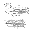
- a flat structure 30 with a conductor track structure according to FIG. 1 is produced from a thin metal foil, which can already be coated on one or both sides with suitable dielectric coverings.
- An essential property of the interconnect structure consisting of four connected substructures 31 to 34 (hereinafter referred to as leaves and in simple sketches also shown as closed leaves) is that, although it appears to be centrally symmetrical about the center 35, all of them are symmetrically opposite with respect to the axis 36 Conductor parts have different widths, so that symmetrical pairs differ in width only by one width jump. 2 shows the cross section through a strip line, consisting of a waveguide track 37, a dielectric of constant thickness 38 and a ground surface 39 which is wider than the width of the waveguide track 37.
- the conductor track structure shown in FIG. 1 is made from uncoated metal foil, this is now done according to the simplified sketch in FIG. 3 with the insertion of the dielectric coverings 40, 41 and 42 along the fold lines 43, 44 and the axis 36 in FIG. 1 folded up, so that there is a cross section through any part of the edge of the folded arrangement shown in FIG. 4. If the conductor track structure shown in FIG. 1 is made from a metal foil which is already laminated beforehand with suitable dielectric coverings 45 and 46, the addition of coverings 40, 41 and 42 is omitted, and a corresponding cross-sectional image is obtained after the analog folding process Fig. 5, a total of a structure with a square structure and openwork interior.
- a Thomsonian oscillation circuit is created with an oscillation circuit capacity, which is composed of the transformation of distributed line capacities and concentrated capacities of the conductor track parts 47 against 48, 47 against 49 and 48 against 50.
- the structure can be described in a first approximation by the equivalent circuit shown in FIG. 6; Corresponding parts and locations are designated there with the same reference numerals as in FIG. 1.
- a high level of positioning accuracy of the individual sheets on top of one another is ensured by forced folding.
- This is achieved in that the conductor track structure according to FIG. 1 is fixed on an endless carrier film 56 during the manufacturing process and in this process in the same tool without dimensional offset to the fixed structure, this together with the carrier film 56 continuously along the lines 43, 44 or the axis 36 is perforated or finely perforated in FIG. 1, so that, according to FIG. 7, perforation lines 57, 58 and 59 are formed along the running direction of the film 56, along which the endless web can be folded up.
- a suitable carrier film 56 e.g. material provided with labeling fields 60 is used, which is provided on the free side with an adhesive or sealing layer 61, which produces different adhesion on the zones inside and outside the perforation lines 57 and 58 and selectively e.g. can be activated by pressure and / or heat.
- the different adhesion by zone means that the sheets 32 and 33 adhere better to the film 56 than the sheets 31 and 34.
- an extremely thin adhesive layer 62 is then applied to the surface of the conductor track structure, but not to the film, as indicated in FIG. 7, which after folding along the perforation lines 57 and 58 between the sheets 31 and 32 and 34 respectively and 33 produces a higher adhesiveness than is initially between the sheets 32 and 33 and the film 56.
- the adhesive or sealing layer 61 in the interior of the remainder 65 of the carrier film 56 remaining as the outer covering is suitably e.g. activated by the action of pressure and / or heat, the structural feature described also ensures that the folded structure between the enveloping coverings is sealed not only from the perforated interior, but also at the outer perforation edges at points 69. This results in a high stability of the arrangement, so that the resulting tape can be rolled up into a supply roll.
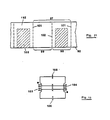
- FIG. 11 shows a cross section through the outer region of an arrangement produced in this way for clarification.
- many thin and flexible resonance elements 70 can be produced by this method, which are introduced into an endless envelope. From this endless belt, they can either be cut off individually or, after a separation perforation 71 and provided with a pressure sensitive adhesive 72 with a release film 73, can be flexibly transferred to objects with automatic roll dispensers.
- the resonance frequency of the arrangement can be kept within predefinable frequency limits regardless of fluctuations in the properties of the dielectrics 45 and 46 or 40, 41 and 42, the adhesive layer 62 or the carrier film 56, as well as other process parameters, as shown in FIG 10 contours 79 of capacitive-acting alignment conductor parts 80 are provided obliquely to the direction of movement of the carrier film and between these conductor path parts 80 a sufficiently wide, insulating tape 81 with a relatively low dielectric constant and sufficient thickness is continuously inserted in the direction of the direction of movement of the carrier film 56.
- the effective circular capacitance and thus the resonance frequency of the finished arrangement can be influenced as a function of the track spacing 82 of this alignment band to the perforation line 59.
- a suitable closed control loop the The actual frequency of manufactured arrangements is recorded without contact, continuously compared with a predetermined target frequency and the dynamics of which can be adjusted to the number of manufactured arrangements per unit of time, so that the compliance with specifiable limits of the resonance frequency can be controlled automatically by regulating the track spacing 82 of this adjustment band.
- the insertion of such an adjustment tape 81 can either be carried out according to FIG. 10 by rolling after the application of the adhesive layer 62 onto the still unfolded structure, taking advantage of the adhesion of this layer 62, or as in FIGS. 8 and 9 indicated, take place in the same way after the first folding using selective adhesive properties of the carrier film 56.
- an increase in inductance with improved shielding can be achieved while maintaining the four-leaf principle according to FIG. 13 by increasing the number of turns of the inner leaves after folding.
- the conductor track parts 83 and 84 acting as capacitor coatings can be arranged such that they come to lie under the two outer halves of the middle conductor track 86 of the structure that was last folded along line 85 and which has the lowest coupling impedance. This further improves the independence of the resonance frequency from capacitive influences.
- Two-layer arrangements with an increased number of turns can be produced quickly and particularly easily by producing a flat conductor track structure 91 consisting of two partial sheets 89 and 90 from a thin metal foil 87, which is provided with a suitable dielectric coating 88, and on one 16 is attached in an adhesive or sealable manner, and this is then folded together according to FIG. 16 together with the conductor track structure thereon along a perforation line 92 which is produced without a dimensional offset and continuously penetrates the conductor path structure and the carrier film in such a way that the dielectric coverings between the conductor paths of the folded-up state are folded together Be included.
- the principle of electrical conduction through a perforation zone along a fold line also applies here. If a metal foil 87 without a dielectric covering 88 is used as the starting material, a dielectric 93 must be inserted between the two partial sheets according to FIG. 16. In this case, too, a Thomsonian oscillation circuit with distributed capacities is created.
- Test patterns showed that fixing the dielectric coverings 88 to one another or the conductor tracks 87 on a dielectric 93 to be inserted by means of a special adhesive layer 62 can be dispensed with if the structure is enclosed in the covering material 65 by means of a suitable sealing layer 61.
- capacitor areas are best designed so that they are elongated in the direction of the turns, since at the same time, as a component of the coil winding, they enable the largest possible induction area with the smallest possible field distortion.
- Such an embodiment can in turn be produced very quickly and easily using the principle of unequal, overlapping conductor track widths for extensive frequency invariance compared to positioning inaccuracies, in that two of each other are provided from a thin metal foil 87, which can also be provided on one side with a suitable dielectric coating 88 17 and made separate, planar structures 109 and 110 according to FIG. 17 and fixed on an adhesive or sealable carrier film 65, which is continuously perforated in the same operation without a dimensional offset between the structures, so that it is shown in FIG.
- an adjustment band 81 is again provided (FIG. 20), which interacts with adjustment surfaces 112, as was explained in detail with reference to FIG. 10.
- the adjustment surfaces 112 are constructed in such a way that there is an approximately quadratic dependence of the adjustment capacity on the parallel displacement of the adjustment band 81 or linear dependence of the resonance frequency on this parallel shift results.
- the identification arrangement described can not only be produced particularly quickly and easily, but also with the least possible waste of raw material, it is particularly suitable for equipping goods labeling and security labels.
- a data-carrying double label 97 consisting of a checkout section 98 equipped with such an identification arrangement and a customer section 99 that is not equipped with it, is produced by using appropriately pre-printed wrapping material suitable as a data carrier 165 and leaving sufficient distances between the structures fixed on this carrier , so that after the folding along the perforation line 92 and the sealing of the carrier, a field equipped with a resonance element 100 and a field that is not equipped therewith alternate in succession.
- This tape is then provided with transverse perforations 101, which follow the incorporated resonance elements, at a fixed distance, for separating individual labels, and an intermediate perforation 102, which is interposed, for separating the customer and checkout sections.
- such a locking mechanism does not have to be inseparably firmly connected to an identification arrangement, and the identification arrangement itself is to be designed as a flexible, resistant, multi-usable label 122, then such can be produced according to FIG. 23 in that the production carrier 165 and thus a sufficiently thick, tear-resistant material with kink-resistant reinforcement is used as the sheathing material of the resonance element, which, if necessary, can be sealed in a tear-resistant manner at the edges of the arrangement by a weld seam 123.
Description
- Die Erfindung betrifft eine Identifizierungsanordnung in Form eines an einem Gegenstand anbringbaren Etiketts, welches wenigstens ein aus flächenhaften Leiterbahnen gebildetes induktives Element und ein aus übereinander angeordneten Leiterbahnen und einem dazwischengefügten Dielektrikum gebildetes kapazitives Element enthält, das mit dem induktiven Element einen Resonanzkreis bildet.
- Die Erfindung betrifft ferner ein Verfahren zur Herstellung einer Identifizierungsanordnung in Form eines an einem Gegenstand anbringbaren Etiketts, weiches wenigstens ein ausflächenhaften Leiterbahnen gebildetes induktives Element und ein aus übereinander angeordneten Leiterbahnteilen und einem dazwischengefügten Dielektrikum gebildetes kapazitives Element enthält, das mit dem induktiven Element einen Resonanzkreis bildet.
- Die Erfindung betrifft schließlich eine Verwendung der oben bezeichneten Identifizierungsanordnung zur Entdeckung von Warendiebstählen.
- Eine Identifizierungsanordnung der eingangs genannten Art ist aus der DE-A-24 23 002 bekannt. Ähnliche Anordnungen sind in der US―A―3 810 147 sowie der GB-A-2 000 382 beschrieben.
- Die bekannten Anordnungen, insbesondere gemäß DE-A-25 23 002, enthalten einen aus flächenhaften Leiterbahnen bestehenden Resonanzkreis, der aus diskreten Elementen aufgebaut ist. Hierunter versteht main einen Resonanzkreis, bei dem die induktiven und die kapazitiven Elemente des Ersatzschaltbildes exakt räumlichen Strukturen der Anordnung zugeordnet werden können. So besteht die bekannte Anordnung gemäß DE-A-25 23 002 beispielsweise aus einem Resonanzkreis mit zwei induktiven und zwei kapazitiven Elementen, wobei die beiden induktiven Elemente durch zwei getrennte flächenhafte, spiralförmige Leiterbahnen gebildet werden, während die kapazitiven Elemente durch jeweils zwei Paare einander in zwei Ebenen gegenüberstehender Leiterflächen gebildet werden.
- Zur Herstellung der erforderlichen diskreten induktiven Elemente ist es bekannt, diese auf flächenartigen Körpern vorzusehen, wie dies beispielsweise in PatentsAbstract of Japan Vol. 5, Nr. 30 vom 24.2. 1981, in der US-A-2 851 765 sowie in der Zeitschrift "Internationale Elektronische Rundschau", Vol. 26, Nr. 5, Mai 1972, Seite 112, beschrieben ist.
- So weist beispielsweise die in der US―A― 3 810 147 beschriebene Identifizierungsanordnung induktive und kapazitive Elemente auf, die in derTechnik gedruckter Leiterplatten durch metallische Leiterbahnen bzw. Leitflächen auf zwei übereinanderliegenden Substratplatten gebildet werden. Die kapazitiven Elemente bestehen dabei aus insgesamt drei Paaren von rechteckförmigen Leitflächen, die auf jeweils beiden Substraten angeordnet sind, während die induktiven Elemente durch spiralförmig angeordnet Leiterbahnen gebildet werden, die beide nur auf einem der beiden Substrate angeordnet sind.
- Die induktiven Elemente einerseits und die kapazitiven Elemente andererseits sind bei dieser bekannten Identifizierungsanordnung somit räumlich voneinander getrennt und nur aus Platzgründen relativ nahe beieinander angeordnet. Eine elektrische Wechselwirkung zwischen diesen Leiterbahnen bzw. Leitflächen über elektromagnetische Felder ist weder vorgesehen noch beabsichtigt.
- Wenn derartige Anordnungen in sehr großer Stückzahl benötigt werden, spielen für die wirtschaftliche Anwendung des Systems die Herstellungkosten eine wesentliche Rolle. Werden beispielsweise die Leiterbahnen auf beiden Seiten einer Trägerfolie ausgebildet, so ist es zur Herstellung galvanischer Verbindungen zwischen den Leiterbahnen oder Leitflächen beider Seiten erforderlich, eine Durchkontaktierung durch dieTrägerfolie hindurch vorzunehmen. Dies giltvorallem im Hinblick auf die induktiven Elemente, die bei den bekannte Identifizierungsanordnungen, wie dies weiter oben anhand der US―A―3810147 beschrieben wurde, als diskretes Bauelement in Gestalt einer spiralförmig verlaufenden Leiterbahn nur auf einem der Substrate angeordnete sind. Hier sind galvanische Verbindungen zwischen den beiden Seiten der Trägerfolie zwingend erforderlich, um den gewünschten Schwingkreis herzustellen.
- Andererseits ist bei den bekannten Anordnungen mit diskret verteilten Elementen auch im Bereich der kapazitiven Elemente mit Schwierigkeiten zu rechnen, wenn die Paßgenauigkeit der Leitflächen auf beiden Seiten der Folie zueinander nicht exakt gewährleistet werden kann. Es ergeben sich dann nämlich merkliche Verschiebungen in den Kapazitätswerten der kapazitiven Elemente und damit Streuungen in der Resonanzfrequenz des insgesamt gebildeten resonanzfähigen Systems.
- Aufgabe der Erfindung ist die Schaffung einer Identifizierungsanordnung und eines Verfahrens zu seiner Herstellung, die eine kostengünstige Massenherstellung ermöglichen, so daß die Identifizierungsanordnungen füreinmaligen Gebrauch geeignetsind. Fernersollen die Identifizierungsanordnungen trotz der kostengünstigen Massenherstellungstechnik geringe Toleranzen und einen hohen Zuverlässiggrad aufweisen.
- Diese Aufgabe wird gemäß der eingangs genannten Anordnung erfindungsgemäß dadurch gelöst, daß die Leiterbahnen als Streifenleitung ausgebildet sind, bei der die das kapazitive Element bildenden Leiterbahnen mindestens teilweise mit Leiterbahnen identisch sind, welche das induktive Element bilden.
- Gemäß dem eingangs genannten Verfahren wird diese Aufgabe erfindungsgemäß dadurch gelöst, daß ein in einer Ebene abwickelbares Leiterbahngebilde längs wenigstens einer Faltlinie so zusammengefaltet wird, daß zwischen wenigstens zwei aufeinander gefalteten Leiterbahnteilen ein Dielektrikum eingefügt wird.
- Schließlich wird die vorstehend genannten Anordnung erfindungsgemäß auch an einem Warenauszeichnungsetikett angeordnet oder das Warenauszeichnungsetikett weist einen Kundenabschnitt und einen mit diesem lösbar verbundenen Kassenabschnitt auf und die Identifizierungsanordnung ist wenigstens in einem der beiden Abschnitte angeordnet.
- Die der Erfindung zugrundeliegende Aufgabe wird auf diese Weise vollkommen gelöst.
- Die Vorteile der vorstehend genannten erfindungsgemäßen Anordnung bestehen vor allem darin, daß bei Verwendung von Streifenleitungen ein wesentlichen größerer Freiheitsgrad hinsichtlich der Durchkontaktierungen besteht, weil bekanntlich Streifenleitungen aus Elementen bestehen, die über elektromagnetische Wellen miteinander in Wirkverbindung stehen. Es ist daher bei derartigen Streifenleitungen grundsätzlich nicht erforderlich, galvanische Verbindungen zwischen einzelnen Substraten herzustellen, weil es eine Eigenheit von Streifenleitungen ist, daß sich nicht aus diskreten Bauelementen-die einer Verdrahtung mit galvanischen Verbindungen bedürften-sondern vielmehr aus infinitesimal verteilten Elementen, nämlich den sogenanten Kapazitätsbelägen und Induktivitätsbelägen bestehen. Außerdem hat sich gezeigt, daß Streifenleitungen der hier interessierenden Art wesentlich weniger anfällig im Hinblick auf Ungenauigkeiten bei der Passung sind, weil die Resonanzfrequenz der Streifenleitung, verglichen mit dem Fall der aus diskreten Bauelementen ausgebauten herkömmlichen Schwingskreise, weniger ändert, wenn die Leitflächen nicht exact zueinander ausgerichtet werden.
- Das genannte erfindungsgemäße Herstellungsverfahren hat den Vorteil, daß unabhängig davon, in welcher Form die Resonanzanordnung aufgebaut ist, eine hochgenaue Passung von Leiterbahnen und insbesondere Leitflächen erzielt werden kann, wenn eine Trägerfolie durch Falten zu einem resonanzfähigen Gebilde gemacht wird, das hinsichtlich der Trägerfolie einstückig ist, so daß beim Falten der Trägerfolie weniger Störungen hinsichtlich der Passung der aufeinandergefalteten Leitflächen auftreten können, als dies bei zwei unabhängigen Folien oder Substraten der Fall wäre, die unabhängig voneinander an einen Montageort gebracht und dort zusammengefügt werden.
- Dem erfindungsgemäßen Verfahren liegt also der Gedanke zugrunde, die Windungen des induktiven Elementes durch Zusammenfalten eines Leiterbahngebildes übereinander anzuordnen, so daß die Anzahl der Windungen praktisch unbegrenzt ist und die erforderlichen verteilten Kapazitäten durch selektives Einfügen von dielektrischen Schichten zwischen aufeinandergefalteten Leiterbahnteilen hergestellt werden können. Da die Leiterbahnen äußerst dünn ausgebildet sein können, kann bei sehr geringer Dicke der gesamten Identifizierungsanordnung ein ausreichend großer Induktivitäts- und Kapazitätswert erreicht werden. Die Ideritifizierungsanordnung kann daher sehr flexibel ausgebildet und insbesondere wie ein herkömmliches Papier-, Kunststoff- oder Pappetikett verarbeitet werden. Da die einzelnen Leiterbahnen bzw. Leitflächen direkt übereinander angeordnet sein können, wird eine ausgezeichnete magnetische Kopplung zwischen den einzelnen Leiterbahnen erreicht, so daß sich geringe Streuinduktivitäten und dadurch genau einhaltbare Transformationsverhältnisse der verteilten Kapazitäten zur gesamtwirksamen Schwingkreiskapazität ergeben.
- Die erfindungsgemäße Identitizierungsanordnung kann sehr flexibel ausgebildet und insbesondere wie ein herkömmliches Papier-, Kunststoff- oder Pappetikett verarbeitet werden.
- Bei eine besonders bevorzugten Ausgestaltung der Erfindung haben die Leiterbahnen in den einander überlagerten Flächen jeweils voneinander verschiedene Formen und/oder Abmessungen, insbesondere unterschiedliche Breiten.
- Diese Maßnahme hat den Vorteil, daß Parallelverschiebungen innerhalb der Herstellungstoleranzen möglich sind, ohne die Resonanzfrequenz des Streifenleitungs-Resonators zu verändern.
- Ausführungsbeispiele der Erfindung sind in der Zeichnung dargestellt und werden nachstehend anhand der Beschreibung näher erläutert. Es zeigen:
- Fig. 1 eine schematische Ansicht eines in eine Ebene abgewickelten Leiterbahngebildes, das nach geeignetem Zusammenfalten ein induktives Element ergibt;
- Fig. 2 eine Schnittansicht einer üblichen Streifenleitung;
- Fig. 3 mehrere schematische Ansichten zur Erläuterung des Zusammenfaltens des Leiterbahngebildes gemäß Fig. 1;
- Fig. 4 und 5 Teilschnittansichten durch das in Fig. 3 gezeigte zusammengefaltete Gebilde;
- Fig. 6 ein Ersatzschaltbild des in den Fig. 3 bis 5 gezeigten elektrischen Bauteils, das einen Parallelresonanzkreis bildet;
- Fig. 7 eine Draufsicht auf eine Trägerfolie, die mehrere Leiterbahngebilde zur Herstellung von Identifizierungsanordnungen trägt;
- Figs. 8, 9 und 10 schematische Ansichten zur Erläuterung weiterer Ausführungsformen der Erfindung, die einen Abgleich des kapazitiven Elements im Verlauf des Herstellungsverfahrens ermöglichen;
- Fig. 11 eine Schnittansicht durch eine randnahe Zone einer fertigen, in eine Schutsfolie eingesiegelten Identifizierungsanordnung;
- Fig. 12 eine schematische Ansicht einer zu einer Vorratsrolle aufgerollten Trägerfolie, in die eine Vielzahl von fertigen elektrischen Identifizierungsanordnungen eingesiegelt ist und die selbsthaftend ausgebildet ist;
- Fig. 13 eine Draufsicht auf ein in eine Ebene abgewickeltes Leiterbahngebilde zur Herstellung einer nach außen abgeschirmten Identifizierungsanordnung mit vier einander überlagerten Ebenen und erhöhter Induktivität;
- Fig. 14 eine Draufsicht auf ein Leiterbahngebilde zur Herstellung einer Identifizierungsanordnung mit acht oder mehr einander überlagerten Faltebenen;
- Figs. 15 und 16 schematische Ansichten zur Erläuterung der Herstellung einer Identifizierungsanordnung mit nur zwei Faltebenen;
- Figs. 17 und 18 schematische Ansichten zur Erläuterung einer Ausführungsform, bei der zwischen zwei einander überlagerten Ebenen nur eine kapazitive Kopplung vorhanden ist;
- Fig. 19 ein Ersatzschaltbild der Ausführungsform nach den Figuren 17 und 18;
- Fig. 20 eine schematische Ansicht zur Erläuterung des Abgleichs des kapazitiven Elements bei der Ausführungsform nach den Figuren 17 und 18 mittels eines dielektrischen Abgleichbandes;
- Fig. 21 eine schematische Draufsicht auf einen streifenförmigen Träger, der abwechselnd je ein mit einer Identifizierungsanordnung versehenes Feld und eine freies Feld aufweist;
- Fig. 22 eine auseinandergezogene Darstellung zur Erläuterung, wie eine erfindungsgemäße Identifizierungsanordnung an einem zu sichernden Gegenstand befestigt werden kann;
- Fig. 23 eine auseinandergezogene Darstellung einer anderen Ausführungsform zur Befestigung einer Identifizierungsanordnung an einem zu sichernden Gegenstand.
- Das Kernstück der erfindungsgemäßen Identifizierungsanordnung ist ein elektrisches Bauteil, das einen Parallelresonanzkreis darstellt und aus einem induktiven Element sowie verteilten Kapazitäten gebildet ist. Im folgenden wird zunächst dieses elektrisches Bauteil beschrieben.
- Da die beschriebene Identizierungsanordnung besonders schnell und einfach, aber auch mit geringstmöglichem Abfall an Rohmaterial hergestellt werden kann, kommt sie ganz besonders zur Ausrüstung von Warenauszeichnungs- und Sicherungsetiketten in Betracht.
- Aus einer dünnen Metallfolie, die ein- oder zweiseitig bereits mit geeigneten dielektrischen Belägen untrennbar beschichtet sein kann, wird eine ebenes Gebilde 30 mit einer Leiterbahnstruktur gemäß Fig. 1 hergestellt. Eine wesentliche Eigenschaft des aus vier zusammenhängenden Teilstrukturen 31 bis 34 (im folgenden als Blätter bezeichnet und in einfachen Skizzen auch als geschlossene Blätter dargestellt) bestehenden Leiterbahngebildes ist, daß es zwar zum Mittelpunkt 35 zentralsymmetrisch angelegt scheint, jedoch alle bezüglich der Achse 36 sich symmetrisch gegenüberliegenden Leiterbahnteile unterschiedliche Breiten aufweisen, so daß sich symmetrische Paare in der Breite jeweils nur um einen Breitensprung unterscheiden. Zur Erläuterung zeigt Fig. 2 den Querschnitt durch eine Streifenleitung, bestehend aus einer Wellenleiterbahn 37, einem Dielektrikum konstanter Dicke 38 und einer Massefläche 39, die ausgedehnter als die Breite der Wellenleiterbahn 37 ist. Wird die Wellenleiterbahn 37 seitlich verschoben, so ändert dies deren Kapazitätzbelag nicht. Wird das in Fig. 1 gezeigte Leiterbahngebilde aus unbeschichteter Metallfolie gefertigt, so wird dieses nun entsprechend der vereinfachten Skizze in Fig. 3 unter Einfügung der dielektrischen Beläge 40, 41 und 42 entlang den Faltlinien 43, 44 bzw. der Achse 36 in Fig. 1 zusammengefaltet, so daß sich ein Querschnitt durch einen beliebigen Teil des Randes der zusammengefalteten Anordnung gemäß Fig. 4 ergibt. Wird das in Fig. 1 gezeigte Leiterbahngebilde aus einer Metallfolie gefertigt, die bereits vorweg mit geeigneten dielektrischen Belägen 45 und 46 kaschiert ist, so entfällt das Einfügen der Beläge 40, 41 und 42, und es ergibt sich nach dem analogen Faltvorgang ein entsprechendes Querschnittsbild gemäß Fig. 5, insgesamt also ein Gebilde mit viereckiger Struktur und durchbrochenem Innern.
- In beiden Fällen entsteht ein Thomsonscher Schwingungskreis mit einer Schwingkreiskapazität, die sich aus der Transformation verteilter Leitungskapazitäten und konzentrierter Kapazitäten der Leiterbahnteile 47 gegen 48, 47 gegen 49 und 48 gegen 50 zusammensetzt. Das Gebilde kann in erster Näherung durch die Ersatzschaltung gemäß Fig. 6 beschrieben werden; einander entsprechende Teile und Orte sind dort mit denselben Bezugszeichen wie in Fig. 1 bezeichnet.
- Die unterschiedliche Breite in zusammengefaltetem Zustand jeweils übereinanderliegender Leiterbahnen leistet mehreres:
- a) Ungenauigkeiten beim Übereinanderpositionieren der einzelnen Blätter ändern die Kapazität zwischen jeweils übereinander verlaufenden Leiterbahnteilen kaum, solange nur eine Positioniertoleranz innerhalb geometrisch einfach bestimmbarer und vorschreibbarer Grenzwerte eingehalten wird. Dieser Effekt kann genutzt werden, solange die Breite der Leiterbahnen viel größer als die Dicke der dielektrischen Trennschichten ist und das elektrisches Feld zwischen Metallbelägen somit überwiegend homogen verläuft. Als Ergebnis ist die wirksame Schwingkreiskapazität gegenüber Positionierungsungenauigkeiten beim Zusammenfalten innerhalb Deckungstoleranzgrenzen praktisch invariant und hängt hauptsächlich von der Maßgenauigkeit der Leiterbahnen und von Eigenschaften des Dielektrikums.
- b) Da die Leiterbahnen sich gegenseitig abdekken, des weiteren die Breite der Leiterbahnen wesentlichen größer als die Dicke der isolierenden Trennschichten zwischen den Windungen der Spule ist, ist die Kopplung der räumlich verteilten Windungen sehr fest und die Streuinduktivität derselben gegeneinander sehr gering. Daraus resultieren sehr konstante Transformationsverhältnisse für die einzelnen verteilten Leitungskapazitäten.
- c) Nach dem Zusammenfalten liegen die Blätter 32. und 33 mit niedriger Impedanz bezogen auf den Strukturmittelpunkt 35 gemäß Fig. 1 bzw. den Spulenmittelpunkt 35 gemäß Fig. 6 auf der Außenseite der Anordnung und schließen die Blätter 31 und 34 mit hoher Impedanz bezogen auf dieselben Punkte in der Art einer statischen Abschirmung im Innern der Anordnung ein, mit der Wirkung, daß das entstehende Gebilde seine Resonanzfrequenz bei kapazitiven Näherungen nur wenig ändert. Die Abzweigungen 51 und 52 sind nicht Bestandteil der eigentlichen Spule, sondern Abschirmflächen niedriger Impedanz, die die Leitungsstücke 53 und 54 mit höherer lmpedanz nach außen abschirmen.
- d) Die außen liegenden Windungen mit größter Leiterbreite, d.h. geringstem Bahnwiderstand, sind die, in denen die größte Stromstärke auftritt. Der Aufbau der Anordnung kommt also auch einer größtmöglichen Kreisgüte entgegen.
- Eine hohe Positioniergenauigkeit der einzelnen Blätter aufeinander wird durch eine erzwungene Faltung gesichert. Diese wird dadurch erreicht, daß das Leiterbahngebilde gemäß Fig. 1 beim Herstellungsprozeß auf einer endlosen Trägerfolie 56 fixiert wird und bei diesem Vorgang im gleichen Werkzeug ohne Maßversatz zum fixierten Gebilde dieses zusammen mit der Trägerfolie 56 fortlaufend längs den Linien 43, 44 bzw. der Achse 36 in Fig. 1 perforiert oder feingelocht wird, so daß gemäß Fig. 7 Perforationslinien 57,58 und 59 längs der Laufrichtung der Folie 56 entstehen, entlang denen die endlose Bahn zusammengefaltet werden kann.
- Diese Perforation wird dabei so ausgeführt,
- -daß eine elektrisch leitende Verbindung durch den Perforationsbereich des Gebildes erhalten bleibt,
- -daß die Längssteifigkeit des Unterlagenmaterials zur Unterstützung einer geführten Faltung ausgenutzt werden kann und
- -daß nicht mehr benötigte Teile der Transportbahn nach einmalig erfolgter Umklappung entlang dieser Perforation abgetrennt werden können.
- Wird zur Herstellung des Gebildes gemäß Fig. 1 als Ausgangsmaterial eine beidseitig dielektrisch beschichtete Metallfolie benutzt, so entfällt das Einfügen der durchgehenden Isolierbeläge 40, 41 und 42 beim Zusammenfalten. Da die wirksamen dielektrischen Schichten gemäß Fig. 5 dann dieselben Konturen aufweisen wie die Leiterbahnen, sind die Innen- und Außenräume der fertig zusammengefalteten Anordnung dann frei von jeglichem Material, so daß das zusammengefaltete Gebilde für sich allein nch keine stabile Form hat.
- Das Herstellen und formstabilisierende Einarbeiten des Bauteils zwischen schützende Deckflächen kann gemäß Fig. 7, Fig. 8 und Fig. 9 dadurch erfolgen, daß als endlose Trägerfolie 56 ein zu diesem Zweck geeignetes, z.B. mit Beschriftungsfeldern 60 versehenes Material benutzt wird, das auf der freien Seite mit einer Haft- oder Siegelschicht 61 ausgerüstet ist, die unterschiedliche Haftung auf den Zonen innerhalb und außerhalb der Perforationslinien 57 und 58 erzeugt und selektiv z.B. durch Druck- und/oder Wärmeeinwirkung aktiviert werden kann. Nach dem Übertragen des aus den Blättern 31 bis 34 bestehenden Gebildes auf eine solche Trägerfolie 56 wird durch die zonenweise unterschiedliche Haftung erreicht, daß die Blätter 32 und 33 auf der Folie 56 zunächst besser haften als die Blätter 31 und 34.
- Mit einem geeigneten Verfahren wird dann auf die Oberfläche des Leiterbahngebildes, nicht jedoch auf die Folie, wie in Fig. 7 angedeutet, eine äußerst dünne Haftschicht 62 angebracht, die nach dem Umfalten längs der Perforationslinien 57 und 58 zwischen den Blättern 31 und 32 bzw 34 und 33 ein höheres Haftvermögen erzeugt, als es zwischen den Blättern 32 und 33 und der Folie 56 zunächst besteht.
- Dies erlaubt nach Ausführung des ersten Faltvorganges längs der Perforationslinien 57 und 58, der die Blätter 31 und 32 bzw. 34 und 33 haftend aufeinander positioniert, gemäß Fig. 8 das Wiederabheben und Abtrennen nicht mehr benötigter Teile 63 und 64 der Trägerfolie 56 längs den Perforationslinien 57 und 58, ohne daß das Leiterbahngebilde vom Rest 65 der Trägerfolie wieder abgehoben wird. Der zweite Faltvorang längs der Perforationslinie 59 positioniert dann die Blätter31 und 34 aufeinander, wie dies in Fig. 9 veranschauchlicht ist.
- Wird nach dem letzten Faltvorgang, der das Gebilde zu einem Resonanzkreis schließt, die Haft-oder Siegelschicht 61 im Innern des Restes 65 der als äußere Umhüllung verbliebenen Trägerfolie 56 in geeigneter Weise z.B. durch Druck- und/oder Wärmeeinwirkung aktiviert, so leistet das beschriebene Strukturmerkmal außerdem, daß das zusammengefaltete Gebilde zwischen den einhüllenden Belägen nicht nur vom durchbrochenen Innenraum her, sondern auch an den außen liegenden Perforationsrändern an Stellen 69 umschliessend eingesiegelt wird. Dadurch wird eine hohe Verschiebestabilität der Anordnung erreicht, so daß das so entstandene Band zu einer Vorratsrolle aufgerollt werden kann.
- Fig. 11 zeigt zur Verdeutlichung einen Querschnitt durch den äußeren Bereich einer auf diese Weise hergestellten Anordnung.
- Gemäß Fig. 12 können nach diesem Verfahren viele dünne und flexible Resonanzelemente 70 hergestellt werden, die in eine endlose Hülle eingebracht sind. Von diesem Endlosband können sie entweder einzeln abgeschnitten oder nach einer Abtrennperforation 71 und Ausrüstung mit einem Haftkleber 72 mit Trennfolie 73 mit automatischen Abrollspendern auf Objekte flexibel übertragen werden.
- In einem fließenden Fertigungsprozeß der beschriebenen Art kann die Resonanzfrequenz der Anordnung unabhängig von auftretenden Schwankungen der Eigenschaften der Dielektrika 45 und 46 bzw. 40, 41 und 42, der Haftschicht 62 oder der Trägerfolie 56 sowie sonstiger Prozeßparameter innerhalb vorgebbarer Frequenzgrenzen gehalten werden, indem gemäß Fig. 10 Konturen 79 kapazitiv wirkender Abgleich-Leiterbahnteile 80 schräg zur Fortbewegungsrichtung derTrägerfolie vorgesehen werden und zwischen diese Leiter- .bahnteile 80 fortlaufend ein ausreichend breites, isolierendes Band 81 mit relativ geringer Dielektrizitätszahl und hinreichender Dicke in Richtung der Fortbewegungsrichtung der Trägerfolie 56 eingefügt wird. Dadurch kann die wirksame Kreiskapazität und somit die Resonanzfrequenz der fertigen Anordnung in Abhängigkeit vom Spurabstand 82 dieses Abgleichbandes zur Perforationslinie 59 beeinflußt werden.
- Ein geeigneter geschlossener Regelkreis, der die Ist-Frequenz gefertigter Anordnungen berührungslos erfaßt, mit einer vorgegebenen SollFrequenz kontinuierlich vergleicht und in seiner Dynamik auf die Zahl gefertigter Anordnungen pro Zeiteinheit abstimmbar ist, kann so über ein Regelung des Spurabstandes 82 diese Abgleichbandes die Einhaltung vorgebbarer Schranken der Resonanzfrequenz automatisch steuern.
- Das Einfügen eines solchen Abgleichbandes 81 kann je nach der gewünschten Abgleichsteilheit entweder gemäß Fig. 10 durch Aufwalzen nach dem Auftrag der Haftschicht 62 auf das noch ungefaltete Gebilde unter Ausnutzung der Haftung eben dieser Schicht 62 oder aber, wie in Fig. 8 und Fig. 9 angedeutet, in gleicher Weise nach der ersten Umfaltung unter Ausnutzung selektiver Hafteigenschaften der Trägerfolie 56 erfolgen.
- Eine Erhöhung der Induktivität bei verbesserter Abschirmung kann unter Beibehaltung des vierblättrigen Prinzips gemäß Fig. 13 durch Erhöhung der Windungszahl der nach dem Zusammenfalten innenliegenden Blätter erreicht werden. Dabei können die als Kondensatorbeläge wirkenden Leiterbahnteile 83 und 84 so angeordnet werden, daß sie unter die beiden außenliegenden Hälften der zuletzt entlang der Linie 85 gefalteten, mitteren Leiterbahn 86 des Gebildes zu liegen kommen, die die niedrigste Ankoppelimpedanz hat. Die Unabhängikeit der Resonanzfrequenz von kapazitiven Näberungseinflüssen wird dadurch weiter verbessert.
- Die gleiche Wirkung wird erzielt, wenn die Struktur mit mehr als vier Lagen ausgeführt wird. Die mögliche Form einer vielblättrigen Struktur, die auch unsymmetrisch nach beiden Seiten mäanderförmig fortgesetzt werden kann, ist in Fig. 14 skizziert. Die erforderliche Abstufung der Leiterbahnbreiten ist hier nur angedeutet.
- Schnell und besonders einfach können zweilagige Anordnungen mit erhöhter windungszahl hergestellt werden, indem aus einer dünnen Metallfolie 87, die mit einem geeigneten dielektrischen Belag 88 versehen ist, gemäß Fig. 15 ein aus zwei Teilblättern 89 und 90 bestehendes, ebenes Leiterbahngebilde 91 hergestellt und auf einer haftend oder siegelbar ausgebildeten Trägerfolie 65a fixiert wird, und dieses dann gemäß Fig. 16 zusammen mit dem darauf befindlichen Leiterbahngebilde entlang einer ohne Maßversatz hergestellten, das Leiterbahngebilde und die Trägerfolie fortlaufend durchdringenden Perforationslinie 92 so zusammengefaltet wird, daß die dielektrischen Beläge zwischen den Leiterbahnen des zusammengefalteten Gebildes eingeschlossen werden. Auch hier findet das Prinzip der elektrischen Leitung durch eine Perforationszone längs einer Faltlinie Anwendung. Wird als Ausgangsmaterial eine Metallfolie 87 ohne dielektrischen Belag 88 benutzt, muß gemäß Fig. 16 ein Dielektrikum 93 zwischen die beiden Teilblätter eingelegt werden. Auch in diesem Fall entsteht ein Thomsonscher Schwingungskreis mit verteilten Kapazitäten.
- Versuchsmuster zeigten, daß ein Fixieren der dielektrischen Beläge 88 aufeinander oder der Leiterbahnen 87 auf einem einzulegenden Dielektrikum 93 durch eine besonders Haftschicht 62 entfallen kann, wenn das Gebilde vermittels einer geeigneten Siegelschicht 61 rundum im Hüllmaterial 65 eingeschlossen wird.
- Auch bei dieser Ausführungsform werden Kondensatorflächen am besten so angelegt, daß sie langgestreckt in Windungsrichtung orientiert sind, da sie so gleichzeitig als Bestandteil der Spulenwicklung eine größtmögliche Induktionsfläche bei kleinstmöglicher Feldverzerrung ermöglichen.
- Bei ausreichender Größe der überlagerten Leiterbahnen können besondere Kondensatorflächen entfallen, so daß die Windungen im Innern der Blattstrukturen dann ohne Abschluß offen enden.
- Wird das Prinzip der elektrischen Leitung durch eine perforierte Zone längs einer Faltlinie aufgegeben und bei der Ausführungsform gemäß Fig. 16 die elektrisch leitende Verbindung längs der Perforationslinie 92 aufgetrennt, so entsteht gemäß Fig. 19 ein Parallelrezonanzkreis mit seriengeteilter Induktivität 103 und 104 und seriengeteilter Kapazität 105 und 106, indem der Kapazitätsbelag zwischen den dann voneinander isolierten Leiterbahnhälften 107 und 108 entlang der Perforationslinie 92 als Serienkondensator 106 wirksam wird. In Fig. 19 sind auch die verteilten Kapazitäten der Windungsflächen gegeneinander angedeutet.
- Eine solche Ausführungsform läßt sich wiederum unter Anwendung des Prinzips ungleicher, sich überdeckender Leiterbahnbreiten für weitgehende Frequenzinvarianz gegenüber Positionierungsungenauigkeiten sehr schnell und einfach herstellen, indem aus einer dünnen Metallfolie 87-die auch einseitig bereits mit einem geeigneten dielektrischen Belag 88 versehen sein kann--zwei voneinander getrennte, ebene Gebilde 109 und 110 gemäß Fig. 17 hergestellt und auf einer haftend oder siegelbar ausgebildeten Trägerfolie 65 fixiert werden, wobei diese im gleichen Arbeitsgang ohne Maßversatz zwischen den Strukturen fortlaufend perforiert wird, so daß sie gemäß Fig. 18 zusammen mit den darauf befindlichen Leiterbahngebilden 109 und 110-erforderlichenfalls unter Einlage eines Dielektrikums 93-entlang der entstehenden Perforationslinie 111 so zusammengefaltet werden kann, daß die beiden Leiterbahngebilde 109 und 110 sich überdecken und über ihre leiterbahnteile 112/113 sowie 114/115 miteinander keine elektrische, sondern nur eine kapazitive Kopplung durch die trennende Isolierschicht 88 oder 93 hindurch haben und das so entstehende Resonanzelement allseitig in der Trägerfolie 56 in der Art einer Schutzhülle eingesiegelt wird. Zur Beeinflussung der Resonanzfrequenz ist wiederum ein Abgleichband 81 vorgesehen (Fig. 20), das mit Abgleichflächen 112 zusammenwirkt, wie im einzelnen anhand der Fig. 10 erläutert wurde. Die Abgleichflächen 112 sind so konstruiert, daß sich eine angenähert quadratische Abhängigkeit der Abgleichkapazität von der Parallelverschiebung des Abgleichbandes 81 bzw. lineare Abhängigkeit der Resonanzfrequenz von dieser Parallelverschiebung ergibt.
- Da die beschriebene Identifizierungsanordnung nicht nur besonders schnell und einfach, sondern ach mit geringstmöglichem Abfall an Rohmaterial hergestellt werden kann, kommt sie ganz besonders zur Ausrüstung von Warenauszeichnungs-und Sicherungsetiketten in Betracht.
- Gemäß Fig. 21 kann zu diesem Zweck z.B. ein datentragendes Auszeichnungsdoppeletikett 97-bestehend aus einem mit einer derartigen Identifizierungsanordnung bestückten Kassenabschnitt 98 und einem damit unausgerüsteten Kundenabschnitt 99-hergestellt werden, indem als Fertigungsträger 165 entsprechend vorbedrucktes, als Datenträger geeignetes Hüllmaterial benutzt wird und ausreichende Abstände zwischen den auf diesen Träger fixierten Strukturen belassen werden, so daß nach dem Zusammenfalten entlang der Perforationslinie 92 und Versiegeln der Trägers jeweils ein mit einem Resonanzelement 100 bestücktes und ein damit unbestücktes Feld abwechselnd aufeinanderfolgen. Dieses Band wird anschießend mit in festem Abstand auf die eingearbeiteten Resonanzelemente folgenden Querperforationen 101 zum Abtrennen einzelner Etiketten und einer jeweils zwischengeschalteten Querperforation 102 zum Auseinandertrennen von Kunden- und Kassenabschnitt versehen.
- Werden Waren- und Preisdaten von derartigen Etiketten nicht manuell, sondern mittels einer eigens dafür vorgesehenen Einrichtung selbsttätig in die Kasse eingegeben, so kann die Einarbeitung eines solchen Resonanzelements auch in den Kundenanschnitt erfolgen, wenn der Kundenabschnitt unmittelbar nach der Registrierung noch im Einlesegerät an geeigneter Stelle durchstanzt und das Resonanzelement im Innern dadurch unwirksam gemacht wird.
- Da diese Anordnung keine Abschirmung nach außen aufweist und Warensicherungsetiketten kleinstmöglich ausgeführt sein sollen, können bei großflächiger Abdeckung mit Gegenständen oder Körperteilen Änderungen der Kreiskapazität und damit der Resonanzfrequenz auftreten.
- Um diesen Effekt geringstmöglich zu halten, werden gemäß bevorzugten Ausführungsformen folgende Maßnahmen getroffen:
- -Das Deckermaterial wird ausreichend dick gewählt, und der wesentliche Teil der Schwingkreiskapazität befindet sich an der Peripherie der Anordnung, d.h. im Kapazitätsbelag zwischen den ersten Windungen beginnen und an der Perforationslinie konzentriert;
- -die Enden der Spule sind nur mit relativ kleinflächigen Kondensatorbelägen abgeschlossen;
- -die Dielektrizitätszahl des Dielektrikums wird möglichst groß und die Dielektrizitätszahl des Hüllmaterials wird möglichst klein gewählt.
- Als Bestandteil elektronischer System zur Entdeckung von Warendiebstählen oder zur Überwachung der Zutriffsbefugnis von Personen sind bereits herkömmliche Anordnungen im Gebrauch, die in einem festen, meist zweiteilig ausgeführten Gehäuse einen Schwingungskreis enthalten, bestehend aus einer Spulenwicklung aus blankem oder isoliertem Draht und einem Kondensator herkömmlicher Bauform, der an die Enden der Spulenwicklung angeschlossen ist.
- Das Einbringen dieser Teile in bisher üblicher Art kann entfallen, indem gemäß Fig. 22 in eine passende, flächenhafte Aussparung 116 im Inneren eines ähnlich gestalteten Gehäuses 117 eine der beschriebenen Resonanzanordnungen 118 eingelegt wird, wobei die papier- oder pappartige Trägerhülse 165 einer solchen Anordnung innerhalb des eingeschlossenen Resonanzgebildes mit einer Lochung 119 versehen sein kann, um einen das gesamte Gehäuse durchdringenden Schließmechanismus 120 aufzunehmen, wie er für wieder lösbare Befestigung des Gesamtgebildes an Kleidungsstücken 121 erforderlich sein kann.
- Wenn ein solcher Schließmechanismus nicht untrennbar fest mit einer Identifikationsanordnung verbunden sein muß, und die Identifikationsanordnung selbst als flexibles, widerstandsfähiges, mehrfach anwendbäres Etikett 122 ausgeführt sein soll, so kann ein solches gemäß Fig. 23 dadurch hergestellt werden, daß als Fertigungsträger 165-und damit als Hüllmaterial des Resonanzelements-ein ausreichend dickes, reißfestes Material mit knickwiderstandsfähiger Armierung benutzt wird, das an der Berandung der Anordnung erforderlichenfalls durch eine Schweißnaht 123 einreißfest versiegelt werden kann.
- Eine ebenfalls durch Umschweißung 124 randverstärkte Bohrung 125 im inneren Teil eines solchen Etiketts kann eine lösbare Befestigung an Handelsware 121 mit üblichen, hierzu geeigneten Vorrichtungen 126 ermöglichen.
Claims (28)
Priority Applications (1)
| Application Number | Priority Date | Filing Date | Title |
|---|---|---|---|
| AT82903167T ATE56554T1 (de) | 1981-10-30 | 1982-10-29 | Identifizierungsanordnung in form eines an einem gegenstand anbringbaren etiketts. |
Applications Claiming Priority (2)
| Application Number | Priority Date | Filing Date | Title |
|---|---|---|---|
| DE3143208A DE3143208C2 (de) | 1981-10-30 | 1981-10-30 | Identifizierungsanordnung in Form eines an einem Gegenstand anbringbaren etikettartigen Streifens und Verfahren zu deren Herstellung |
| DE3143208 | 1981-10-30 |
Publications (2)
| Publication Number | Publication Date |
|---|---|
| EP0092555A1 EP0092555A1 (de) | 1983-11-02 |
| EP0092555B1 true EP0092555B1 (de) | 1990-09-12 |
Family
ID=6145268
Family Applications (1)
| Application Number | Title | Priority Date | Filing Date |
|---|---|---|---|
| EP82903167A Expired - Lifetime EP0092555B1 (de) | 1981-10-30 | 1982-10-29 | Identifizierungsanordnung in form eines an einem gegenstand anbringbaren etiketts |
Country Status (7)
| Country | Link |
|---|---|
| US (2) | US4694283A (de) |
| EP (1) | EP0092555B1 (de) |
| JP (1) | JPS58501843A (de) |
| AT (1) | ATE56554T1 (de) |
| DE (2) | DE3143208C2 (de) |
| DK (1) | DK285283A (de) |
| WO (1) | WO1983001697A1 (de) |
Cited By (2)
| Publication number | Priority date | Publication date | Assignee | Title |
|---|---|---|---|---|
| DE19963130A1 (de) * | 1999-12-24 | 2001-06-28 | Meto International Gmbh | Zu verschiedenen elektronischen Artikelüberwachungssystemen kompatible Sicherungseinrichtung und Verfahren zum Sichern von Artikeln |
| DE10019410A1 (de) * | 2000-04-19 | 2001-10-31 | Daimler Chrysler Ag | Flexibler Flachleiter |
Families Citing this family (108)
| Publication number | Priority date | Publication date | Assignee | Title |
|---|---|---|---|---|
| US5291180A (en) * | 1981-10-30 | 1994-03-01 | Reeb Max E | LC structure useful in radio frequency security systems |
| US5285191A (en) * | 1981-10-30 | 1994-02-08 | Reeb Max E | LC marker construction useful as an electromagnetically interrogatable transponder means |
| DE3221500A1 (de) * | 1982-06-07 | 1983-12-08 | Max-E. Dipl.-Ing. 7320 Göppingen Reeb | Identifizierungsanordnung in form eines an einem gegenstand anbringbaren gebildes und verfahren zur herstellung |
| DE3337787A1 (de) * | 1983-09-16 | 1985-04-04 | Volex AG, Zürich | Schwingkreis fuer eine gegen diebstahl zu sichernde ware, verfahren zur herstellung eines schwingkreises und einrichtung zur ausfuehrung des verfahrens |
| DE3340469A1 (de) * | 1983-11-09 | 1985-05-15 | Guido 8944 Grönenbach Dorn | Warenetikett |
| DK163151C (da) * | 1983-11-16 | 1992-06-22 | Minnesota Mining & Mfg | Maerkeplade med lc resonanskredsloeb til anvendelse i elektronisk genstandsovervaagningssystem, fremgangsmaade til fremstilling af maerkeplader, samt elektronisk genstandsovervaagningssystem hvori maerkepladen anvendes. |
| US4578654A (en) * | 1983-11-16 | 1986-03-25 | Minnesota Mining And Manufacturing Company | Distributed capacitance lc resonant circuit |
| US4598276A (en) * | 1983-11-16 | 1986-07-01 | Minnesota Mining And Manufacturing Company | Distributed capacitance LC resonant circuit |
| US4583099A (en) * | 1983-12-27 | 1986-04-15 | Polyonics Corporation | Resonant tag circuits useful in electronic security systems |
| US4658264A (en) * | 1984-11-09 | 1987-04-14 | Minnesota Mining And Manufacturing Company | Folded RF marker for electronic article surveillance systems |
| DE3508369A1 (de) * | 1985-03-08 | 1986-09-11 | Max-E. Dipl.-Ing. 7336 Uhingen Reeb | Etikettartiges gebilde und verfahren zu seiner herstellung |
| JPH0325264Y2 (de) * | 1985-09-30 | 1991-05-31 | ||
| CH677988A5 (de) * | 1986-07-30 | 1991-07-15 | Actron Entwicklungs Ag | |
| NL8700388A (nl) * | 1987-02-17 | 1988-09-16 | Nedap Nv | Flexibele identificatielabel. |
| US4772878A (en) * | 1987-05-06 | 1988-09-20 | Kane Roger A | Merchandise theft deterrent sensor |
| ZA888680B (en) * | 1987-11-20 | 1990-07-25 | Magellan Corp Australia | Capacitor construction |
| AU626539B2 (en) * | 1988-03-11 | 1992-08-06 | Magellan Corporation (Australia) Pty Ltd | Resonant circuit with a foldable dielectric layer and conductive strip |
| WO1989008973A1 (en) * | 1988-03-11 | 1989-09-21 | Magellan Corporation (Australia) Pty. Ltd. | Inductive element and method of manufacture |
| EP0428907B1 (de) * | 1989-10-26 | 1995-08-16 | Takeshi Ikeda | LC-Störfilter |
| GB9007132D0 (en) * | 1990-03-30 | 1990-05-30 | Gen Foods Kraft Ltd | Packages containing comestibles |
| US5103210A (en) * | 1990-06-27 | 1992-04-07 | Checkpoint Systems, Inc. | Activatable/deactivatable security tag for use with an electronic security system |
| US5695860A (en) * | 1990-08-06 | 1997-12-09 | Tokai Electronics Co., Ltd. | Resonant tag and method of manufacturing the same |
| US5447779A (en) * | 1990-08-06 | 1995-09-05 | Tokai Electronics Co., Ltd. | Resonant tag and method of manufacturing the same |
| JP3096069B2 (ja) * | 1990-08-06 | 2000-10-10 | チェックポイント・マニュファクチュアリング・ジャパン株式会社 | 共振タグ及びその製造方法 |
| US5589251A (en) * | 1990-08-06 | 1996-12-31 | Tokai Electronics Co., Ltd. | Resonant tag and method of manufacturing the same |
| US5075671A (en) * | 1991-03-11 | 1991-12-24 | Livingston Iii Robert | Personal alarm system |
| US5151684A (en) * | 1991-04-12 | 1992-09-29 | Johnsen Edward L | Electronic inventory label and security apparatus |
| US5241299A (en) * | 1991-05-22 | 1993-08-31 | Checkpoint Systems, Inc. | Stabilized resonant tag circuit |
| US5218189A (en) * | 1991-09-09 | 1993-06-08 | Checkpoint Systems, Inc. | Binary encoded multiple frequency rf indentification tag |
| US5315289A (en) * | 1991-09-16 | 1994-05-24 | Fuller Terry A | Anticipatory interactive protective system |
| US5182544A (en) * | 1991-10-23 | 1993-01-26 | Checkpoint Systems, Inc. | Security tag with electrostatic protection |
| ATE136674T1 (de) * | 1991-12-19 | 1996-04-15 | Ake Gustafson | Sicherheitsverschliessvorrichtung |
| US5252918A (en) * | 1991-12-20 | 1993-10-12 | Halliburton Company | Apparatus and method for electromagnetically detecting the passing of a plug released into a well by a bridge circuit |
| US5253821A (en) * | 1992-03-02 | 1993-10-19 | Minnesota Mining And Manufacturing Company | Security magnetic tape cartridge for use in electronic article surveillance systems |
| US5565778A (en) * | 1992-06-01 | 1996-10-15 | Conductus, Inc. | Nuclear magnetic resonance probe coil |
| DE4220002A1 (de) * | 1992-06-19 | 1993-12-23 | Esselte Meto Int Gmbh | Thermodrucker |
| US5357240A (en) * | 1992-10-16 | 1994-10-18 | Sensormatic Electronics Corporation | EAS tag with mechanically vibrating magnetic element and improved housing and method of making same |
| US5323856A (en) * | 1993-03-31 | 1994-06-28 | Halliburton Company | Detecting system and method for oil or gas well |
| US5428346A (en) * | 1993-05-28 | 1995-06-27 | Sealed Air Corporation | Theft alarm activating absorbent pad |
| US5444223A (en) * | 1994-01-11 | 1995-08-22 | Blama; Michael J. | Radio frequency identification tag and method |
| FI98866C (fi) * | 1994-04-06 | 1997-08-25 | Tuotesuoja Sirpa Jaervensivu K | Tuotesuoja-anturi |
| DE4415801A1 (de) * | 1994-05-05 | 1994-09-22 | Siegfried Mehl | Diebstahlsicherungselement |
| DE59506506D1 (de) * | 1994-05-10 | 1999-09-09 | Meto International Gmbh | Sicherheitsetikettenstreifen |
| DE4416444C2 (de) * | 1994-05-10 | 2003-06-26 | Meto International Gmbh | Sicherheitsetikettenstreifen |
| JP2969426B2 (ja) * | 1994-07-26 | 1999-11-02 | 株式会社サニー・シーリング | 共振ラベル及びその製造方法 |
| US6496382B1 (en) | 1995-05-19 | 2002-12-17 | Kasten Chase Applied Research Limited | Radio frequency identification tag |
| CA2176625C (en) | 1995-05-19 | 2008-07-15 | Donald Harold Fergusen | Radio frequency identification tag |
| JP2000515683A (ja) * | 1996-07-18 | 2000-11-21 | フランソワ デュロ | プリント回路を製造する方法およびこの方法に従って製造されるプリント回路 |
| US6466131B1 (en) * | 1996-07-30 | 2002-10-15 | Micron Technology, Inc. | Radio frequency data communications device with adjustable receiver sensitivity and method |
| DE19708180A1 (de) * | 1996-11-04 | 1998-05-07 | Esselte Meto Int Gmbh | Sicherungselement für die elektronische Artikelüberwachung |
| AU723358B2 (en) * | 1996-11-04 | 2000-08-24 | Meto International Gmbh | Security element for electronic article surveillance |
| US6025725A (en) * | 1996-12-05 | 2000-02-15 | Massachusetts Institute Of Technology | Electrically active resonant structures for wireless monitoring and control |
| US6222452B1 (en) * | 1996-12-16 | 2001-04-24 | Confidence International Ab | Electronic identification tag |
| US6304169B1 (en) | 1997-01-02 | 2001-10-16 | C. W. Over Solutions, Inc. | Inductor-capacitor resonant circuits and improved methods of using same |
| US6395373B2 (en) | 1998-02-11 | 2002-05-28 | Avery Dennison Corporation | Label/tag with embedded signaling device and method and apparatus for making and using |
| US6006198A (en) * | 1998-02-20 | 1999-12-21 | Newland, Jr.; Ross G. | System and method for detecting merchandise sliding and under ringing at cash register |
| US8585852B2 (en) * | 1999-06-16 | 2013-11-19 | Vanguard Identification Systems, Inc. | Methods of making printed planar radio frequency identification elements |
| US8654018B2 (en) * | 2005-04-06 | 2014-02-18 | Vanguard Identificaiton Systems, Inc. | Printed planar RFID element wristbands and like personal identification devices |
| US6597175B1 (en) | 1999-09-07 | 2003-07-22 | Halliburton Energy Services, Inc. | Electromagnetic detector apparatus and method for oil or gas well, and circuit-bearing displaceable object to be detected therein |
| DE19951561A1 (de) * | 1999-10-27 | 2001-05-03 | Meto International Gmbh | Sicherungselement für die elektronischen Artikelsicherung |
| US6751847B1 (en) | 1999-11-04 | 2004-06-22 | Fsu Research Foundation, Inc. | Laser-assisted fabrication of NMR resonators |
| DE19955464A1 (de) * | 1999-11-08 | 2001-07-19 | Heinz Brych | Vorrichtung zur Detektion und Identifikation von Gegenständen |
| US6254953B1 (en) | 1999-12-02 | 2001-07-03 | World Color Printing Division, Inc. | Antitheft hang tag folded and secured to conceal antitheft marker |
| US6806812B1 (en) * | 2000-04-26 | 2004-10-19 | Micron Technology, Inc. | Automated antenna trim for transmitting and receiving semiconductor devices |
| US6806842B2 (en) * | 2000-07-18 | 2004-10-19 | Marconi Intellectual Property (Us) Inc. | Wireless communication device and method for discs |
| US7098850B2 (en) * | 2000-07-18 | 2006-08-29 | King Patrick F | Grounded antenna for a wireless communication device and method |
| US6483473B1 (en) * | 2000-07-18 | 2002-11-19 | Marconi Communications Inc. | Wireless communication device and method |
| USRE47599E1 (en) | 2000-10-20 | 2019-09-10 | Promega Corporation | RF point of sale and delivery method and system using communication with remote computer and having features to read a large number of RF tags |
| US20020183882A1 (en) | 2000-10-20 | 2002-12-05 | Michael Dearing | RF point of sale and delivery method and system using communication with remote computer and having features to read a large number of RF tags |
| US7258276B2 (en) | 2000-10-20 | 2007-08-21 | Promega Corporation | Radio frequency identification method and system of distributing products |
| AU2001297814A1 (en) * | 2000-12-22 | 2002-07-08 | Bent Thorning Bensen A/S | Sensing device, method of its production, and use |
| US6407669B1 (en) * | 2001-02-02 | 2002-06-18 | 3M Innovative Properties Company | RFID tag device and method of manufacturing |
| US7017820B1 (en) | 2001-02-08 | 2006-03-28 | James Brunner | Machine and process for manufacturing a label with a security element |
| FR2824018B1 (fr) * | 2001-04-26 | 2003-07-04 | Arjo Wiggins Sa | Couverture incorporant un dispositif d'identification radiofrequence |
| US6693541B2 (en) | 2001-07-19 | 2004-02-17 | 3M Innovative Properties Co | RFID tag with bridge circuit assembly and methods of use |
| US6891474B1 (en) | 2001-08-01 | 2005-05-10 | Tagsense, Inc. | Electromagnetic identification label for anti-counterfeiting, authentication, and tamper-protection |
| US6724311B1 (en) | 2001-11-09 | 2004-04-20 | B&G Plastics, Inc. | Anti-theft hang tag |
| US8339265B2 (en) | 2002-01-09 | 2012-12-25 | Sensormatic Electronics, Llc. | Method of assigning and deducing the location of articles detected by multiple RFID antennae |
| US7084769B2 (en) * | 2002-01-09 | 2006-08-01 | Vue Technology, Inc. | Intelligent station using multiple RF antennae and inventory control system and method incorporating same |
| DE10204884A1 (de) * | 2002-02-06 | 2003-08-14 | Schreiner Gmbh & Co Kg | Transponderetikett |
| AU2003233033A1 (en) * | 2002-04-24 | 2003-11-10 | Marconi Intellectual Property (Us) Inc | Manufacturing method for a wireless communication device and manufacturing apparatus |
| US20030214388A1 (en) * | 2002-05-20 | 2003-11-20 | Stuart James Riley | RFID deployment system |
| US20040069847A1 (en) * | 2002-10-15 | 2004-04-15 | Chester Kolton | Electronic article surveillance marker assembly |
| JP2004207700A (ja) * | 2002-12-11 | 2004-07-22 | Canon Inc | 電子部品およびその製造方法 |
| US7270353B2 (en) * | 2003-02-24 | 2007-09-18 | The European Community | Multiple transponder seal device |
| US6969277B2 (en) * | 2003-10-06 | 2005-11-29 | Shackelford Richard A | Electrical insulating bands |
| US7768405B2 (en) | 2003-12-12 | 2010-08-03 | Semiconductor Energy Laboratory Co., Ltd | Semiconductor device and manufacturing method thereof |
| US7573390B2 (en) * | 2004-03-15 | 2009-08-11 | Iwata Label Co., Ltd. | Split-able label |
| US8519846B2 (en) * | 2004-03-16 | 2013-08-27 | Newage Industries, Inc. | Tracking system for gamma radiation sterilized bags and disposable items |
| US7268687B2 (en) * | 2004-03-23 | 2007-09-11 | 3M Innovative Properties Company | Radio frequency identification tags with compensating elements |
| US7350703B2 (en) * | 2004-04-23 | 2008-04-01 | Ambartsoumian Gourgen | Low temperature radio frequency identification tracking system |
| JP2008511234A (ja) * | 2004-08-26 | 2008-04-10 | コーニンクレッカ フィリップス エレクトロニクス エヌ ヴィ | 折返しダイポールを有するrfidタグ |
| US20060116602A1 (en) * | 2004-12-01 | 2006-06-01 | Alden Dana A | Medical sensing device and system |
| CA2599973A1 (en) * | 2005-03-03 | 2006-09-08 | Vue Technology, Inc. | Apparatus for and method of using an intelligent network and rfid signal router |
| US7897528B2 (en) * | 2005-05-31 | 2011-03-01 | Mikhail Finkel | Heat resistant labels |
| US7348885B2 (en) * | 2005-08-19 | 2008-03-25 | Printronix, Inc. | Capacitively-coupled RFID encoder |
| US8316156B2 (en) * | 2006-02-17 | 2012-11-20 | Intel-Ne, Inc. | Method and apparatus for interfacing device drivers to single multi-function adapter |
| US20080074262A1 (en) * | 2006-09-20 | 2008-03-27 | Paulkovich Michael B | Asset protection system and method |
| CA2616696A1 (en) | 2006-12-29 | 2008-06-29 | Vanguard Identification Systems, Inc. | Printed planar rfid element wristbands and like personal identification devices |
| US7710275B2 (en) | 2007-03-16 | 2010-05-04 | Promega Corporation | RFID reader enclosure and man-o-war RFID reader system |
| US8089362B2 (en) * | 2009-04-08 | 2012-01-03 | Avery Dennison Corporation | Merchandise security kit |
| CN103109165B (zh) | 2010-04-08 | 2015-08-19 | 捷通国际有限公司 | 销售点感应系统和方法 |
| US20140232503A1 (en) * | 2013-02-21 | 2014-08-21 | Pulse Electronics, Inc. | Flexible substrate inductive apparatus and methods |
| JP5592554B1 (ja) | 2013-12-18 | 2014-09-17 | 武延 本郷 | 冷間圧接装置、コイル製造装置、コイルおよびその製造方法 |
| EP4230337A3 (de) | 2013-12-18 | 2023-11-15 | Aster Co., Ltd. | Vorrichtung zur herstellung einer spule und spulenherstellungsverfahren |
| US9380698B1 (en) * | 2014-12-05 | 2016-06-28 | VivaLnk, Inc. | Stretchable electronic patch having a foldable circuit layer |
| US9378450B1 (en) * | 2014-12-05 | 2016-06-28 | Vivalnk, Inc | Stretchable electronic patch having a circuit layer undulating in the thickness direction |
| CN117034997A (zh) * | 2017-10-24 | 2023-11-10 | 艾利丹尼森零售信息服务公司 | 折叠时形成用于rfid标签的线圈的平面导电器件 |
Family Cites Families (7)
| Publication number | Priority date | Publication date | Assignee | Title |
|---|---|---|---|---|
| US2851765A (en) * | 1954-07-29 | 1958-09-16 | Hanlet Jacques Marie Noel | Electrical windings |
| CH483685A (de) | 1967-07-25 | 1969-12-31 | Hasler Ag | Maschinell lesbare Etikette |
| US3810147A (en) * | 1971-12-30 | 1974-05-07 | G Lichtblau | Electronic security system |
| DE2403670A1 (de) | 1974-01-10 | 1975-07-24 | Erich Kwoka | Etikett |
| US4187509A (en) * | 1977-06-20 | 1980-02-05 | Knogo Corporation | Wafer and fastener for use in electronic theft detection system |
| US4311992A (en) * | 1979-07-02 | 1982-01-19 | Eaton Corporation | Reusable releasable fastener |
| US4369557A (en) * | 1980-08-06 | 1983-01-25 | Jan Vandebult | Process for fabricating resonant tag circuit constructions |
-
1981
- 1981-10-30 DE DE3143208A patent/DE3143208C2/de not_active Expired
-
1982
- 1982-10-29 WO PCT/DE1982/000210 patent/WO1983001697A1/de active IP Right Grant
- 1982-10-29 EP EP82903167A patent/EP0092555B1/de not_active Expired - Lifetime
- 1982-10-29 AT AT82903167T patent/ATE56554T1/de not_active IP Right Cessation
- 1982-10-29 JP JP82503223A patent/JPS58501843A/ja active Pending
- 1982-10-29 DE DE8282903167T patent/DE3280241D1/de not_active Expired - Fee Related
- 1982-10-29 US US06/513,970 patent/US4694283A/en not_active Expired - Lifetime
-
1983
- 1983-06-21 DK DK285283A patent/DK285283A/da not_active Application Discontinuation
-
1987
- 1987-12-18 US US07/135,547 patent/US4990891A/en not_active Expired - Fee Related
Cited By (3)
| Publication number | Priority date | Publication date | Assignee | Title |
|---|---|---|---|---|
| DE19963130A1 (de) * | 1999-12-24 | 2001-06-28 | Meto International Gmbh | Zu verschiedenen elektronischen Artikelüberwachungssystemen kompatible Sicherungseinrichtung und Verfahren zum Sichern von Artikeln |
| DE10019410A1 (de) * | 2000-04-19 | 2001-10-31 | Daimler Chrysler Ag | Flexibler Flachleiter |
| DE10019410B4 (de) * | 2000-04-19 | 2005-07-14 | Daimlerchrysler Ag | Flexibler Flachleiter |
Also Published As
| Publication number | Publication date |
|---|---|
| DK285283D0 (da) | 1983-06-21 |
| DE3143208A1 (de) | 1983-05-19 |
| EP0092555A1 (de) | 1983-11-02 |
| US4694283A (en) | 1987-09-15 |
| US4990891A (en) | 1991-02-05 |
| ATE56554T1 (de) | 1990-09-15 |
| WO1983001697A1 (fr) | 1983-05-11 |
| DK285283A (da) | 1983-06-21 |
| DE3280241D1 (de) | 1990-10-18 |
| JPS58501843A (ja) | 1983-10-27 |
| DE3143208C2 (de) | 1984-07-05 |
Similar Documents
| Publication | Publication Date | Title |
|---|---|---|
| EP0092555B1 (de) | Identifizierungsanordnung in form eines an einem gegenstand anbringbaren etiketts | |
| WO1983004448A1 (fr) | Dispositif d'identification en forme d'etiquette pouvant etre appliquee sur un objet et son procede de fabrication | |
| DE60116079T2 (de) | Strommessvorrichtung | |
| DE3590698C2 (de) | ||
| DE2333813C3 (de) | Ebene Magnetkopfanordnung mit mehreren flachen Magnetkopfstrukturen | |
| EP0255073B1 (de) | Schaltungsanordnung und Resonanzetikette sowie Verfahren zu ihrer Herstellung | |
| EP1372106B1 (de) | System aus Wickelkernen mit Wickelbändern und einem Schreib-/Lesegerät, welches zum berührungslosen Auslesen und/oder Überschreiben von Daten dient | |
| DE3732825C2 (de) | Kontinuierliches Verfahren (von Rolle zu Rolle) zum Herstellen einer Vielzahl von Anhängern bzw. Etiketten | |
| DE3912840A1 (de) | Suchspulenanordnung fuer ein induktives suchgeraet | |
| DE3912697A1 (de) | Stoerschutzfilter | |
| EP1527413B1 (de) | Datenträger mit transponderspule | |
| DE3423139A1 (de) | Monolithische induktivitaet mit transformatoranwendungen | |
| DE4428732C1 (de) | Mehrlagige Chipkartenspulen für kontaktfreie Chipkarten | |
| DE3143210A1 (de) | "elektrisches bauteil" | |
| DE60130572T2 (de) | Induktive bauelemente | |
| EP0919049B1 (de) | Resonanzschwingkreis für die elektronische artikelsicherung | |
| DE4306416A1 (de) | Spulenstruktur für eine Leiterplattenanordnung | |
| DE3322004A1 (de) | Induktives element, insbesondere uebertrager | |
| DE3247425C2 (de) | ||
| EP0848261A2 (de) | Sonde zur Erfassung von magnetischen Wechselfeldern | |
| DE602005003990T2 (de) | RF Transponder und Verfahren zur Frequenzabstimmung | |
| DE3312680A1 (de) | Spulenanordnung | |
| EP0473970B1 (de) | Verfahren zur Herstellung von elektrischen Schwingkreisen, insbesondere Resonanz-Etiketten | |
| EP1017033B1 (de) | Sicherungselement für die elektronische Artikelsicherung und Verfahren zur Herstellung eines Sicherungselementes | |
| DE10019410B4 (de) | Flexibler Flachleiter |
Legal Events
| Date | Code | Title | Description |
|---|---|---|---|
| PUAI | Public reference made under article 153(3) epc to a published international application that has entered the european phase |
Free format text: ORIGINAL CODE: 0009012 |
|
| AK | Designated contracting states |
Designated state(s): AT BE CH DE FR GB LI LU NL SE |
|
| 17P | Request for examination filed |
Effective date: 19831028 |
|
| RAP1 | Party data changed (applicant data changed or rights of an application transferred) |
Owner name: REEB, MAX E. |
|
| RAP1 | Party data changed (applicant data changed or rights of an application transferred) |
Owner name: SCHUCK, PETER H. Owner name: BLIKLE, HEINZ |
|
| RIN1 | Information on inventor provided before grant (corrected) |
Inventor name: REEB, MAX E. |
|
| RAP1 | Party data changed (applicant data changed or rights of an application transferred) |
Owner name: REEB, MAX E. |
|
| RIN1 | Information on inventor provided before grant (corrected) |
Inventor name: REEB, MAX E. |
|
| GRAA | (expected) grant |
Free format text: ORIGINAL CODE: 0009210 |
|
| AK | Designated contracting states |
Kind code of ref document: B1 Designated state(s): AT BE CH DE FR GB LI LU NL SE |
|
| PG25 | Lapsed in a contracting state [announced via postgrant information from national office to epo] |
Ref country code: SE Effective date: 19900912 Ref country code: NL Effective date: 19900912 Ref country code: BE Effective date: 19900912 |
|
| REF | Corresponds to: |
Ref document number: 56554 Country of ref document: AT Date of ref document: 19900915 Kind code of ref document: T |
|
| REF | Corresponds to: |
Ref document number: 3280241 Country of ref document: DE Date of ref document: 19901018 |
|
| PG25 | Lapsed in a contracting state [announced via postgrant information from national office to epo] |
Ref country code: AT Effective date: 19901029 |
|
| PG25 | Lapsed in a contracting state [announced via postgrant information from national office to epo] |
Ref country code: LU Free format text: LAPSE BECAUSE OF NON-PAYMENT OF DUE FEES Effective date: 19901031 |
|
| ET | Fr: translation filed | ||
| GBT | Gb: translation of ep patent filed (gb section 77(6)(a)/1977) | ||
| NLV1 | Nl: lapsed or annulled due to failure to fulfill the requirements of art. 29p and 29m of the patents act | ||
| PLBI | Opposition filed |
Free format text: ORIGINAL CODE: 0009260 |
|
| 26 | Opposition filed |
Opponent name: MONARCH MARKING SYSTEMS Effective date: 19910603 |
|
| PLAB | Opposition data, opponent's data or that of the opponent's representative modified |
Free format text: ORIGINAL CODE: 0009299OPPO |
|
| R26 | Opposition filed (corrected) |
Opponent name: MONARCH MARKING SYSTEMS, INC. Effective date: 19910603 |
|
| PGFP | Annual fee paid to national office [announced via postgrant information from national office to epo] |
Ref country code: DE Payment date: 19961231 Year of fee payment: 15 |
|
| PGFP | Annual fee paid to national office [announced via postgrant information from national office to epo] |
Ref country code: CH Payment date: 19970131 Year of fee payment: 15 |
|
| PGFP | Annual fee paid to national office [announced via postgrant information from national office to epo] |
Ref country code: GB Payment date: 19971028 Year of fee payment: 16 |
|
| PG25 | Lapsed in a contracting state [announced via postgrant information from national office to epo] |
Ref country code: LI Free format text: LAPSE BECAUSE OF NON-PAYMENT OF DUE FEES Effective date: 19971031 Ref country code: CH Free format text: LAPSE BECAUSE OF NON-PAYMENT OF DUE FEES Effective date: 19971031 |
|
| PGFP | Annual fee paid to national office [announced via postgrant information from national office to epo] |
Ref country code: FR Payment date: 19971203 Year of fee payment: 16 |
|
| REG | Reference to a national code |
Ref country code: CH Ref legal event code: PL |
|
| PG25 | Lapsed in a contracting state [announced via postgrant information from national office to epo] |
Ref country code: DE Free format text: LAPSE BECAUSE OF NON-PAYMENT OF DUE FEES Effective date: 19980701 |
|
| PG25 | Lapsed in a contracting state [announced via postgrant information from national office to epo] |
Ref country code: GB Free format text: LAPSE BECAUSE OF NON-PAYMENT OF DUE FEES Effective date: 19981029 |
|
| GBPC | Gb: european patent ceased through non-payment of renewal fee |
Effective date: 19981029 |
|
| PG25 | Lapsed in a contracting state [announced via postgrant information from national office to epo] |
Ref country code: FR Free format text: LAPSE BECAUSE OF NON-PAYMENT OF DUE FEES Effective date: 19990630 |
|
| REG | Reference to a national code |
Ref country code: FR Ref legal event code: ST |
|
| RAP2 | Party data changed (patent owner data changed or rights of a patent transferred) |
Owner name: REEB, MAX E. |
|
| RIN2 | Information on inventor provided after grant (corrected) |
Free format text: REEB, MAX E. |
|
| PLBL | Opposition procedure terminated |
Free format text: ORIGINAL CODE: EPIDOS OPPC |
|
| PLBM | Termination of opposition procedure: date of legal effect published |
Free format text: ORIGINAL CODE: 0009276 |
|
| STAA | Information on the status of an ep patent application or granted ep patent |
Free format text: STATUS: OPPOSITION PROCEDURE CLOSED |
|
| 27C | Opposition proceedings terminated |
Effective date: 20000921 |
|
| PLAB | Opposition data, opponent's data or that of the opponent's representative modified |
Free format text: ORIGINAL CODE: 0009299OPPO |