EP0091256A2 - CMOS-Anordnung - Google Patents
CMOS-Anordnung Download PDFInfo
- Publication number
- EP0091256A2 EP0091256A2 EP83301735A EP83301735A EP0091256A2 EP 0091256 A2 EP0091256 A2 EP 0091256A2 EP 83301735 A EP83301735 A EP 83301735A EP 83301735 A EP83301735 A EP 83301735A EP 0091256 A2 EP0091256 A2 EP 0091256A2
- Authority
- EP
- European Patent Office
- Prior art keywords
- transistor
- impurity region
- semiconductor body
- impurity
- region
- Prior art date
- Legal status (The legal status is an assumption and is not a legal conclusion. Google has not performed a legal analysis and makes no representation as to the accuracy of the status listed.)
- Granted
Links
Images


Classifications
-
- H—ELECTRICITY
- H10—SEMICONDUCTOR DEVICES; ELECTRIC SOLID-STATE DEVICES NOT OTHERWISE PROVIDED FOR
- H10P—GENERIC PROCESSES OR APPARATUS FOR THE MANUFACTURE OR TREATMENT OF DEVICES COVERED BY CLASS H10
- H10P30/00—Ion implantation into wafers, substrates or parts of devices
- H10P30/20—Ion implantation into wafers, substrates or parts of devices into semiconductor materials, e.g. for doping
- H10P30/202—Ion implantation into wafers, substrates or parts of devices into semiconductor materials, e.g. for doping characterised by the semiconductor materials
- H10P30/204—Ion implantation into wafers, substrates or parts of devices into semiconductor materials, e.g. for doping characterised by the semiconductor materials into Group IV semiconductors
-
- H—ELECTRICITY
- H10—SEMICONDUCTOR DEVICES; ELECTRIC SOLID-STATE DEVICES NOT OTHERWISE PROVIDED FOR
- H10D—INORGANIC ELECTRIC SEMICONDUCTOR DEVICES
- H10D84/00—Integrated devices formed in or on semiconductor substrates that comprise only semiconducting layers, e.g. on Si wafers or on GaAs-on-Si wafers
- H10D84/01—Manufacture or treatment
- H10D84/0123—Integrating together multiple components covered by H10D12/00 or H10D30/00, e.g. integrating multiple IGBTs
- H10D84/0126—Integrating together multiple components covered by H10D12/00 or H10D30/00, e.g. integrating multiple IGBTs the components including insulated gates, e.g. IGFETs
- H10D84/0165—Integrating together multiple components covered by H10D12/00 or H10D30/00, e.g. integrating multiple IGBTs the components including insulated gates, e.g. IGFETs the components including complementary IGFETs, e.g. CMOS devices
- H10D84/0188—Manufacturing their isolation regions
-
- H—ELECTRICITY
- H10—SEMICONDUCTOR DEVICES; ELECTRIC SOLID-STATE DEVICES NOT OTHERWISE PROVIDED FOR
- H10D—INORGANIC ELECTRIC SEMICONDUCTOR DEVICES
- H10D84/00—Integrated devices formed in or on semiconductor substrates that comprise only semiconducting layers, e.g. on Si wafers or on GaAs-on-Si wafers
- H10D84/01—Manufacture or treatment
- H10D84/02—Manufacture or treatment characterised by using material-based technologies
- H10D84/03—Manufacture or treatment characterised by using material-based technologies using Group IV technology, e.g. silicon technology or silicon-carbide [SiC] technology
- H10D84/038—Manufacture or treatment characterised by using material-based technologies using Group IV technology, e.g. silicon technology or silicon-carbide [SiC] technology using silicon technology, e.g. SiGe
-
- H—ELECTRICITY
- H10—SEMICONDUCTOR DEVICES; ELECTRIC SOLID-STATE DEVICES NOT OTHERWISE PROVIDED FOR
- H10D—INORGANIC ELECTRIC SEMICONDUCTOR DEVICES
- H10D84/00—Integrated devices formed in or on semiconductor substrates that comprise only semiconducting layers, e.g. on Si wafers or on GaAs-on-Si wafers
- H10D84/80—Integrated devices formed in or on semiconductor substrates that comprise only semiconducting layers, e.g. on Si wafers or on GaAs-on-Si wafers characterised by the integration of at least one component covered by groups H10D12/00 or H10D30/00, e.g. integration of IGFETs
- H10D84/82—Integrated devices formed in or on semiconductor substrates that comprise only semiconducting layers, e.g. on Si wafers or on GaAs-on-Si wafers characterised by the integration of at least one component covered by groups H10D12/00 or H10D30/00, e.g. integration of IGFETs of only field-effect components
- H10D84/83—Integrated devices formed in or on semiconductor substrates that comprise only semiconducting layers, e.g. on Si wafers or on GaAs-on-Si wafers characterised by the integration of at least one component covered by groups H10D12/00 or H10D30/00, e.g. integration of IGFETs of only field-effect components of only insulated-gate FETs [IGFET]
- H10D84/85—Complementary IGFETs, e.g. CMOS
- H10D84/858—Complementary IGFETs, e.g. CMOS comprising a P-type well but not an N-type well
-
- H—ELECTRICITY
- H10—SEMICONDUCTOR DEVICES; ELECTRIC SOLID-STATE DEVICES NOT OTHERWISE PROVIDED FOR
- H10P—GENERIC PROCESSES OR APPARATUS FOR THE MANUFACTURE OR TREATMENT OF DEVICES COVERED BY CLASS H10
- H10P30/00—Ion implantation into wafers, substrates or parts of devices
- H10P30/20—Ion implantation into wafers, substrates or parts of devices into semiconductor materials, e.g. for doping
- H10P30/21—Ion implantation into wafers, substrates or parts of devices into semiconductor materials, e.g. for doping of electrically active species
- H10P30/212—Through-implantation
Definitions
- the present invention relates to a semiconductor device, more particularly to a complementary metal oxide semiconductor (CMOS) integrated circuit (IC) having a p-type island and an n-type island.
- CMOS complementary metal oxide semiconductor
- CMOS IC offers the advantage of high speed operation, it is therefore drawing attention as a semiconductor device suited for large-scale integration and for reducing element sizes.
- CMOS IC has a problem with its operation characteristics, i.e., withstand voltage.
- FET field-effect transistor
- Fig. 1 is a schematic cross-sectional view of an n-channel MOS field-effect transistor (FET) according to a prior art.
- FET field-effect transistor
- a and B Two n-channel MOS FET's, indicated by A and B, are formed on a p-type silicon substrate 1.
- p-type channel cut diffusion layers 3 n type diffusion layers 4a and 4b, n type diffusion layers 5, and p + type diffusion layers 6 are formed.
- Reference numeral 2 is a silicon dioxide film, on which polycrystalline silicon gates 7 are formed.
- n type diffusion layers 4a which act as source and drain layers are formed remote from the gate. Further, the n -type high resistance diffusion layer 5 is formed between the gate region 7 and the n type diffusion layer 4a.
- the depletion region of the n - -type diffusion layer 5 is expanded so as to decrease the electric field relative to the gate electrode.
- the silicon substrate 1 is used as is without forming a channel cut diffusion region.
- the p + diffusion layer 6 is formed with a high impurity concentration.
- the channel cut diffusion region may be connected to the n + -type diffusion layers 4b, as indicated by B, to enhance the degree of integration.
- CMOS IC's are subject to the following two adiditional factors.
- the limit on the operation voltage of 4 varies depending upon the impurity concentration in the vicinity of source and drain diffusion layers, i.e., the withstand voltage increases with a decrease in the impurity concentration in the vicinity of the source and drain diffusion layers. With regard to 6 and 7, however, the withstand voltage generally decreases with a decrease of the impurity concentration. To increase the integration density, it is often required to form transistors in the regions of high impurity concentrations.
- a semiconductor device comprising:
- the first and third transistor are p channel MOS transistor and the second transistor is n channel MOS transistor.
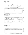
- FIGS. 2A to 2D illustrate steps of manufacturing a MOS FET in a region of low impurity concentration on the surface of a silicon substrate.
- the same portions are denoted by the same reference numerals.
- a silicon dioxide (Si0 2 ) film 22 is first formed on the surface of an n-type silicon substrate 21 by the thermal oxidation method. Then, a resist film 23 for patterning marks 24 of a mask for ion injection is formed. The positioning marks 24, which have a criss-cross shape viewed from above, are next formed by etching.
- the resist film 23 is removed and the silicon dioxide film 22 is grown again by the thermal oxidation method.
- Another resist film 25 is formed and an n-type well region is patterned.
- Phosphorus ions (P + ) are injected by the ion implantation method under an acceleration energy of 20 to 200 KeV and a dosage of 2 x 10 12 to 2 x 10 14 cm -2 .
- a resist film 26 is formed and patterning is effected to form a p-type well region.
- Boron ions (B + ) are then implanted by the ion implantation method.
- the boron ions are implanted under an acceleration energy of 20 to 200 KeV and a dosage of 2 x 10 12 to 14 2 x 10 14 cm -2 .
- impurity diffusion layers 27 and 28 are next formed by heat treatment of about 1200°C.
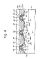
- channel-cutting diffusion layers 43, 46 and 46A are formed by the ion implantation method, as shown in Fig. 4, an oxide film 22A is formed on the field regions, and a gate oxide film 22B is formed after an oxide film 22 has been removed.
- Polycrystalline silicon gates 41, an oxide film 22C, phosphosilicate glass (PSG) film 47, and aluminum electrodes 42 are formed.
- the device is covered with a PSG film 48 to complete the CMOS IC.
- a silicon dioxide film 22 is formed by the thermal oxidation on the surface of an n-type silicon substrate 21.
- a nitride film 29 is formed to a thickness of about 1,000 nm.
- the nitride film 29 is patterned to form active regions, a pattern for forming an n-type well region is formed by a resist film 34, and phosphorus ions are implanted by the ion implantation method under an acceleration energy of 100 to 300 KeV and a dosage of 2 x 10 12 to 2 x 1014cm-2.
- a pattern 35 for forming a p-type well region is formed.
- Boron ions are implanted by the ion implantation method under an acceleration energy of 50 to 200 KeV and a dosage of 2 x 10 12 to 2 x 10 14 cm -2 .
- impurity diffusion layers 27 and 28 are formed by heat treatment. Therefore, the MOS FET is formed in the same manner as the case of producing conventional CMOS IC's, thereby completing the CMOS IC illustrated in Fig. 4.
- a central MOS FET among three MOS FET's is formed on a portion of the silicon substrate 21 where no well region is formed and where the impurity concentration is low. Further, the central MOS FET has no channel-cut diffusion layer 43 or 46, unlike the two other MOS FET's, and, hence, exhibits increased withstand voltage. Compared with the two other transistors, furthermore, the central transistor can have an increased gate width, although the drawing illustrates the same width. The gate width can in practice be increased from the conventional width of 2 to 3 pm (microns) to as great as about 6 ⁇ m. Accordingly, the central transistor exhibits improved characteristics against the punch-through effect. Furthermore, the central MOS FET of Fig. 4 may be used as a high withstand voltage MOS FET indicated by A in Fig. 1.
Landscapes
- Metal-Oxide And Bipolar Metal-Oxide Semiconductor Integrated Circuits (AREA)
Applications Claiming Priority (2)
| Application Number | Priority Date | Filing Date | Title |
|---|---|---|---|
| JP53072/82 | 1982-03-31 | ||
| JP57053072A JPS58170047A (ja) | 1982-03-31 | 1982-03-31 | 半導体装置 |
Publications (3)
| Publication Number | Publication Date |
|---|---|
| EP0091256A2 true EP0091256A2 (de) | 1983-10-12 |
| EP0091256A3 EP0091256A3 (en) | 1985-09-11 |
| EP0091256B1 EP0091256B1 (de) | 1989-08-09 |
Family
ID=12932605
Family Applications (1)
| Application Number | Title | Priority Date | Filing Date |
|---|---|---|---|
| EP83301735A Expired EP0091256B1 (de) | 1982-03-31 | 1983-03-28 | CMOS-Anordnung |
Country Status (3)
| Country | Link |
|---|---|
| EP (1) | EP0091256B1 (de) |
| JP (1) | JPS58170047A (de) |
| DE (1) | DE3380384D1 (de) |
Cited By (8)
| Publication number | Priority date | Publication date | Assignee | Title |
|---|---|---|---|---|
| EP0182876A4 (de) * | 1984-05-25 | 1986-11-10 | American Micro Syst | Drei-wannen cmos-technologie. |
| EP0178991A3 (en) * | 1984-10-13 | 1986-12-03 | Fujitsu Limited | A complementary semiconductor device having high switching speed and latchup-free capability |
| US4697332A (en) * | 1984-05-25 | 1987-10-06 | Gould Inc. | Method of making tri-well CMOS by self-aligned process |
| EP0404026A3 (de) * | 1989-06-22 | 1991-07-10 | Siemens Aktiengesellschaft | Schaltung zur Reduzierung der Latch-up Empfindlichkeit eines CMOS-Schaltkreises |
| EP0762492A1 (de) * | 1995-08-25 | 1997-03-12 | Sony Corporation | Halbleiterelement-Herstellungsverfahren |
| EP0951075A1 (de) * | 1998-04-17 | 1999-10-20 | Matsushita Electronics Corporation | Halbleiterbauelement mit p-n Übergang und Methode zu dessen Steuerung |
| US6091116A (en) * | 1994-05-17 | 2000-07-18 | Samsung Electronics Co., Ltd. | CMOS device and method for manufacturing the same |
| US6406955B1 (en) | 1994-05-17 | 2002-06-18 | Samsung Electronics Co., Ltd | Method for manufacturing CMOS devices having transistors with mutually different punch-through voltage characteristics |
Families Citing this family (2)
| Publication number | Priority date | Publication date | Assignee | Title |
|---|---|---|---|---|
| JPS63136661A (ja) * | 1986-11-28 | 1988-06-08 | Sony Corp | 半導体装置の製造方法 |
| EP0730305A1 (de) * | 1995-02-28 | 1996-09-04 | STMicroelectronics S.r.l. | Hochspannungs-N-Kanal-MOSFET in CMOS-Typ-Technologie und Herstellungsverfahren |
Family Cites Families (1)
| Publication number | Priority date | Publication date | Assignee | Title |
|---|---|---|---|---|
| JPS5787161A (en) * | 1980-11-20 | 1982-05-31 | Seiko Epson Corp | Mos integrated circuit |
-
1982
- 1982-03-31 JP JP57053072A patent/JPS58170047A/ja active Pending
-
1983
- 1983-03-28 DE DE8383301735T patent/DE3380384D1/de not_active Expired
- 1983-03-28 EP EP83301735A patent/EP0091256B1/de not_active Expired
Cited By (11)
| Publication number | Priority date | Publication date | Assignee | Title |
|---|---|---|---|---|
| EP0182876A4 (de) * | 1984-05-25 | 1986-11-10 | American Micro Syst | Drei-wannen cmos-technologie. |
| US4697332A (en) * | 1984-05-25 | 1987-10-06 | Gould Inc. | Method of making tri-well CMOS by self-aligned process |
| EP0178991A3 (en) * | 1984-10-13 | 1986-12-03 | Fujitsu Limited | A complementary semiconductor device having high switching speed and latchup-free capability |
| US4893164A (en) * | 1984-10-13 | 1990-01-09 | Fujitsu Limited | Complementary semiconductor device having high switching speed and latchup-free capability |
| EP0404026A3 (de) * | 1989-06-22 | 1991-07-10 | Siemens Aktiengesellschaft | Schaltung zur Reduzierung der Latch-up Empfindlichkeit eines CMOS-Schaltkreises |
| US6091116A (en) * | 1994-05-17 | 2000-07-18 | Samsung Electronics Co., Ltd. | CMOS device and method for manufacturing the same |
| US6406955B1 (en) | 1994-05-17 | 2002-06-18 | Samsung Electronics Co., Ltd | Method for manufacturing CMOS devices having transistors with mutually different punch-through voltage characteristics |
| EP0762492A1 (de) * | 1995-08-25 | 1997-03-12 | Sony Corporation | Halbleiterelement-Herstellungsverfahren |
| EP0951075A1 (de) * | 1998-04-17 | 1999-10-20 | Matsushita Electronics Corporation | Halbleiterbauelement mit p-n Übergang und Methode zu dessen Steuerung |
| US6388308B1 (en) | 1998-04-17 | 2002-05-14 | Matsushita Electric Industrial Co., Ltd. | Semiconductor device and method for driving the same |
| US6686641B2 (en) | 1998-04-17 | 2004-02-03 | Matsushita Electric Industrial Co., Ltd. | Semiconductor device and method for driving the same |
Also Published As
| Publication number | Publication date |
|---|---|
| EP0091256A3 (en) | 1985-09-11 |
| EP0091256B1 (de) | 1989-08-09 |
| DE3380384D1 (en) | 1989-09-14 |
| JPS58170047A (ja) | 1983-10-06 |
Similar Documents
| Publication | Publication Date | Title |
|---|---|---|
| US5688722A (en) | CMOS integrated circuit with reduced susceptibility to PMOS punchthrough | |
| US5427964A (en) | Insulated gate field effect transistor and method for fabricating | |
| EP0596468A2 (de) | MOSFET vom LDD-Typ und Verfahren zur Herstellung | |
| JPH07321216A (ja) | Cmosおよびその製造方法 | |
| EP0676809A2 (de) | Feldeffekttransistor mit isoliertem Gate und Herstellungsverfahren | |
| JP2000286346A (ja) | 半導体装置およびその製造方法 | |
| JP3206026B2 (ja) | 高電圧用misfetを備える半導体装置 | |
| JPS58147074A (ja) | 金属酸化物半導体トランジスタデバイス及びその製法 | |
| US4229756A (en) | Ultra high speed complementary MOS device | |
| EP0091256B1 (de) | CMOS-Anordnung | |
| US4713329A (en) | Well mask for CMOS process | |
| JPH0730107A (ja) | 高耐圧トランジスタ及びその製造方法 | |
| KR0139773B1 (ko) | 반도체 집적 회로 장치 및 그 제조 방법 | |
| JPH11284178A (ja) | 絶縁ゲートトランジスタ及びその製造方法並びに半導体集積回路装置 | |
| JPH0230185A (ja) | 半導体装置とその製造方法 | |
| JP2003249567A (ja) | 半導体装置 | |
| EP1225627A2 (de) | Integrierter Halbleiterschaltkreis und zugehöriges Herstellungsverfahren | |
| JP2953915B2 (ja) | 半導体集積回路装置及びその製造方法 | |
| JPH07254645A (ja) | 半導体装置の製造方法 | |
| JPH0927556A (ja) | 半導体集積回路装置およびその製造方法 | |
| JPS63302562A (ja) | Mos型半導体装置の製造方法 | |
| JP3216110B2 (ja) | 相補型半導体装置の製造方法 | |
| JP3017838B2 (ja) | 半導体装置およびその製造方法 | |
| KR930001562B1 (ko) | 반도체 집적 회로장치의 제조방법 | |
| JP2002343884A (ja) | 半導体装置およびその製造方法 |
Legal Events
| Date | Code | Title | Description |
|---|---|---|---|
| PUAI | Public reference made under article 153(3) epc to a published international application that has entered the european phase |
Free format text: ORIGINAL CODE: 0009012 |
|
| AK | Designated contracting states |
Designated state(s): DE FR GB |
|
| PUAL | Search report despatched |
Free format text: ORIGINAL CODE: 0009013 |
|
| AK | Designated contracting states |
Designated state(s): DE FR GB |
|
| 17P | Request for examination filed |
Effective date: 19860220 |
|
| 17Q | First examination report despatched |
Effective date: 19870807 |
|
| GRAA | (expected) grant |
Free format text: ORIGINAL CODE: 0009210 |
|
| AK | Designated contracting states |
Kind code of ref document: B1 Designated state(s): DE FR GB |
|
| REF | Corresponds to: |
Ref document number: 3380384 Country of ref document: DE Date of ref document: 19890914 |
|
| ET | Fr: translation filed | ||
| PLBE | No opposition filed within time limit |
Free format text: ORIGINAL CODE: 0009261 |
|
| STAA | Information on the status of an ep patent application or granted ep patent |
Free format text: STATUS: NO OPPOSITION FILED WITHIN TIME LIMIT |
|
| 26N | No opposition filed | ||
| PGFP | Annual fee paid to national office [announced via postgrant information from national office to epo] |
Ref country code: GB Payment date: 19930105 Year of fee payment: 11 |
|
| PGFP | Annual fee paid to national office [announced via postgrant information from national office to epo] |
Ref country code: FR Payment date: 19930330 Year of fee payment: 11 |
|
| PGFP | Annual fee paid to national office [announced via postgrant information from national office to epo] |
Ref country code: DE Payment date: 19930521 Year of fee payment: 11 |
|
| PG25 | Lapsed in a contracting state [announced via postgrant information from national office to epo] |
Ref country code: GB Effective date: 19940328 |
|
| GBPC | Gb: european patent ceased through non-payment of renewal fee |
Effective date: 19940328 |
|
| PG25 | Lapsed in a contracting state [announced via postgrant information from national office to epo] |
Ref country code: FR Effective date: 19941130 |
|
| PG25 | Lapsed in a contracting state [announced via postgrant information from national office to epo] |
Ref country code: DE Effective date: 19941201 |
|
| REG | Reference to a national code |
Ref country code: FR Ref legal event code: ST |