EP0951075A1 - Halbleiterbauelement mit p-n Übergang und Methode zu dessen Steuerung - Google Patents
Halbleiterbauelement mit p-n Übergang und Methode zu dessen Steuerung Download PDFInfo
- Publication number
- EP0951075A1 EP0951075A1 EP99102307A EP99102307A EP0951075A1 EP 0951075 A1 EP0951075 A1 EP 0951075A1 EP 99102307 A EP99102307 A EP 99102307A EP 99102307 A EP99102307 A EP 99102307A EP 0951075 A1 EP0951075 A1 EP 0951075A1
- Authority
- EP
- European Patent Office
- Prior art keywords
- doped layer
- electrode
- region
- semiconductor
- semiconductor substrate
- Prior art date
- Legal status (The legal status is an assumption and is not a legal conclusion. Google has not performed a legal analysis and makes no representation as to the accuracy of the status listed.)
- Withdrawn
Links
Images


Classifications
-
- H—ELECTRICITY
- H10—SEMICONDUCTOR DEVICES; ELECTRIC SOLID-STATE DEVICES NOT OTHERWISE PROVIDED FOR
- H10D—INORGANIC ELECTRIC SEMICONDUCTOR DEVICES
- H10D8/00—Diodes
- H10D8/01—Manufacture or treatment
- H10D8/021—Manufacture or treatment of breakdown diodes
- H10D8/022—Manufacture or treatment of breakdown diodes of Zener diodes
-
- H—ELECTRICITY
- H10—SEMICONDUCTOR DEVICES; ELECTRIC SOLID-STATE DEVICES NOT OTHERWISE PROVIDED FOR
- H10D—INORGANIC ELECTRIC SEMICONDUCTOR DEVICES
- H10D62/00—Semiconductor bodies, or regions thereof, of devices having potential barriers
- H10D62/10—Shapes, relative sizes or dispositions of the regions of the semiconductor bodies; Shapes of the semiconductor bodies
- H10D62/102—Constructional design considerations for preventing surface leakage or controlling electric field concentration
- H10D62/112—Constructional design considerations for preventing surface leakage or controlling electric field concentration for preventing surface leakage due to surface inversion layers, e.g. by using channel stoppers
-
- H—ELECTRICITY
- H10—SEMICONDUCTOR DEVICES; ELECTRIC SOLID-STATE DEVICES NOT OTHERWISE PROVIDED FOR
- H10D—INORGANIC ELECTRIC SEMICONDUCTOR DEVICES
- H10D8/00—Diodes
- H10D8/20—Breakdown diodes, e.g. avalanche diodes
- H10D8/25—Zener diodes
Definitions
- the present invention generally relates to a semiconductor device used for a semiconductor integrated circuit, and more particularly relates to a constant voltage device used as a semiconductor internal voltage booster, for example.
- a constant voltage device called “clamping diode” has heretofore been used to fix a voltage, which has been increased by a semiconductor internal voltage booster, at a desired constant voltage.
- a clamping diode is also termed “zener diode”, which is used for obtaining a desired constant voltage by utilizing a reverse breakdown phenomenon at a pn junction between a semiconductor substrate and a doped layer formed on the semiconductor substrate.
- zener diode which is used for obtaining a desired constant voltage by utilizing a reverse breakdown phenomenon at a pn junction between a semiconductor substrate and a doped layer formed on the semiconductor substrate.
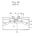
- Figure 10 is a cross-sectional view illustrating an exemplary structure of a conventional semiconductor device functioning as a constant voltage device.
- a field oxide 2 is formed on a P-type semiconductor substrate 1 so as to surround and define an active region 3 .
- a P-type doped layer 4 is formed as a channel stopper just under the field oxide 2 , and an N-type doped layer 5 is formed in the active region 3 .
- An interlevel dielectric film 6 is formed over the substrate. And the N-type doped layer 5 is connected to an aluminum interconnect 7 through an opening of the interlevel dielectric film 6 .
- the constant voltage device is configured in such a manner that the desired constant voltage thereof is determined by a reverse breakdown voltage of the pn junction between the N-type and P-type doped layers 5 and 4 .
- a reverse voltage, exceeding the constant voltage is applied to the region between the aluminum interconnect 7 and the P-type semiconductor substrate 1 , reverse current flows between the N-type and P-type doped layers 5 and 4 due to the zener effect or avalanche effect.
- the voltage between the aluminum interconnect 7 and the P-type semiconductor substrate 1 is substantially fixed at a constant voltage.
- the conventional configuration has the following problems.
- a higher voltage should be applied between the N-type doped layer 5 (or the aluminum interconnect 7 ) and the substrate 1 to increase the voltage between the P-type and N-type doped layers 4 and 5 up to the reverse breakdown voltage at the pn junction.
- a voltage between the N-type doped layer 5 (or the aluminum interconnect 7 ) and the substrate 1 required to cause the breakdown of the pn junction, will be referred to as a "reverse withstand voltage”.
- the total quantity of holes trapped also increases.
- the reverse withstand voltage further increases with the passage of time, i.e., varies as represented by the plot identified with X in Figure 4 . It should be noted that electrons might be possibly trapped in the vicinity of the interface between the field oxide 2 and the P-type doped layer 4 depending on the specific structure of the semiconductor device. In such a case, the reverse withstand voltage continuously decreases with time.
- the overall performance of the semiconductor device as a constant voltage device deteriorates with time, because the reverse withstand voltage is variable from the desired constant voltage.
- a prime object of the present invention is providing a semiconductor device as a constant voltage device that can suppress the variation in reverse withstand voltage with time by taking various measures.
- a first semiconductor device includes: a semiconductor substrate; a semiconductor region of a first conductivity type formed in the semiconductor substrate; a doped layer of a second conductivity type formed in the semiconductor region; an isolating insulator film formed on the semiconductor substrate so as to surround the doped layer; a first electrode in contact with the doped layer; and a second electrode formed at least on the isolating insulator film and made of a conductor film in the vicinity of the doped layer.
- the quantity of carriers trapped in the interface between the isolating insulator film and the semiconductor region can be reduced by regulating the voltage applied to the second electrode. Accordingly, a semiconductor device having a function of suppressing the variation in reverse withstand voltage can be obtained.
- the second electrode is preferably formed on part of the isolating insulator film, the part including at least an end of the isolating insulator film.
- the isolating insulator film may be at least partially spaced apart from the doped layer with an offset region interposed therebetween, and the second electrode may overlap the isolating insulator film and the offset region.
- At least part of the interface between the isolating insulator film and the semiconductor region is offset from the pn junction where electron-hole pairs are created. Accordingly, the quantity of holes or electrons trapped in the vicinity of the interface can be reduced. As a result, a semiconductor device having a superior function of suppressing the variation in reverse withstand voltage can be obtained.
- the second electrode may be connected to a ground terminal.
- the second electrode may be connected to a power supply terminal.
- the second electrode may be connected to the power supply terminal via a resistor.
- the second electrode may be connected to the doped layer.
- the semiconductor device may further include a channel stopper region formed under the isolating insulator film in the semiconductor region and heavily doped with a dopant of the first conductivity type.
- a semiconductor device exhibiting smaller variation in reverse withstand voltage with time can be formed by regulating the reverse withstand voltage using the channel stopper enhancing the isolation function.
- the semiconductor device may further include a reverse withstand voltage regulating region formed between the doped layer and the channel stopper region in the semiconductor region and doped with a dopant of the first conductivity type more heavily than the semiconductor region and more lightly than the channel stopper region.
- the initial value of the reverse withstand voltage can be regulated, and the charge quantity per unit volume of the electron-hole pairs created and trapped can be reduced. Accordingly, it is possible to suppress the variation in reverse withstand voltage with time.
- a second semiconductor device includes: a semiconductor substrate; a semiconductor region of a first conductivity type formed in the semiconductor substrate; a doped layer of a second conductivity type formed in the semiconductor region; an isolating insulator film formed on the semiconductor substrate so as to surround the doped layer; and an electrode in contact with the doped layer.
- the isolating insulator film is at least partially spaced apart from the doped layer with an offset region interposed therebetween.
- At least part of the interface between the isolating insulator film and the semiconductor region is offset from the pn junction where electron-hole pairs are created. Accordingly, the quantity of holes or electrons trapped in the vicinity of the interface can be reduced. As a result, a semiconductor device having a superior function of suppressing the variation in reverse withstand voltage can be obtained.
- the semiconductor device may further include a channel stopper region formed under the isolating insulator film in the semiconductor region and heavily doped with a dopant of the first conductivity type.
- the semiconductor device preferably further includes a reverse withstand voltage regulating region formed between the doped layer and the channel stopper region in the semiconductor region, and doped with a dopant of the first conductivity type more heavily than the semiconductor region and more lightly than the channel stopper region.
- a first method according to the present invention is a method for driving a semiconductor device including: a semiconductor substrate; a semiconductor region of a first conductivity type formed in the semiconductor substrate; a doped layer of a second conductivity type formed in the semiconductor region; an isolating insulator film formed on the semiconductor substrate so as to surround the doped layer; a first electrode in contact with the doped layer; and a second electrode formed at least on the isolating insulator film and made of a conductor film in the vicinity of the doped layer.
- a potential in the second electrode is controlled such that a reverse withstand voltage between the doped layer and the semiconductor region falls within a predetermined range.
- a second method is a method for driving a semiconductor device including: a semiconductor substrate; a semiconductor region of a first conductivity type formed in the semiconductor substrate; a doped layer of a second conductivity type formed in the semiconductor region; an isolating insulator film formed on the semiconductor substrate so as to surround the doped layer; a first electrode in contact with the doped layer; and a second electrode formed at least on the isolating insulator film and made of a conductor film in the vicinity of the doped layer.
- a voltage for reducing carriers trapped in an interface between the isolating insulator film and the semiconductor region is intermittently applied to the second electrode.
- the voltage can be refreshed at the initial value thereof.
- the device may be operated for a predetermined amount of time with the second electrode held at a first potential selected from the group consisting of: a ground potential; a power supply potential; and a potential of the doped layer. And then the second electrode may be biased at a second potential selected from the group excluding the first potential.
- the second electrode may be alternately and repeatedly biased at the first and second potentials.
- the second electrode may be biased at the first and second potentials cyclically and alternately showing positive and negative values.
- carrier trapping can be suppressed and refreshing for reducing the quantity of carriers trapped can be performed.
- Figures 1 and 2 are respectively cross-sectional view and plan view of the semiconductor device in this embodiment.
- the device includes: a P-type semiconductor substrate 11 ; a field oxide (isolating insulator film) 12 ; an active region 13 ; a P-type doped layer 14 ; an N-type doped layer 15 ; and a thin oxide film 16 formed over the active region 13 .
- the field oxide 12 is formed by a LOCOS technique on the substrate 11 to surround the active region 13 in the shape of a regular octagon.
- the P-type doped layer 14 is formed as a channel stopper just under the field oxide 12 by being heavily doped with a P-type dopant.
- the N-type doped layer 15 is formed in the center portion of the active region 13 by being heavily doped with an N-type dopant.
- the inner peripheral end of the field oxide 12 is spaced apart from the N-type doped layer 15 with a predetermined gap.
- An electrode 17 made of polycrystalline silicon in the shape of a regular octagonal ring is provided to overlap the field oxide 12 and the oxide film 16 .
- An interlevel dielectric film 18 is also deposited over the substrate.
- first and second aluminum interconnects 20 and 21 are formed on the interlevel dielectric film 18 to make electrical contact with the N-type doped layer 15 and the electrode 17 , respectively, though contact holes 19 formed in the interlevel dielectric film 18 .
- the first aluminum interconnect 20 functions as the first electrode, while the electrode 17 functions as the second electrode.
- a reverse withstand voltage regulating region 25 is also formed to surround the N-type doped layer 15 and make contact with the P-type doped layer 14 in the semiconductor substrate 11 by being doping with a P-type dopant.
- the dopant concentrations in the N-type doped layer 15 , the reverse withstand voltage regulating region 25 and the P-type doped layer 14 are on the orders of 10 2 0 /cm 3 , 10 1 7 /cm 3 and 10 1 8 /cm 3 , respectively.
- the active region 13 is shaped like a regular octagon where a pair of opposed sides are spaced from each other by a distance of about 10 ⁇ m to about 40 ⁇ m.
- the gap between the inner peripheral end of the field oxide 12 and the N-type doped layer 15 is about 2 ⁇ m.
- the outer periphery of the N-type doped layer 15 is substantially aligned with the inner periphery of the electrode 17 .
- a desired constant voltage required for operating the semiconductor device as a constant voltage device is obtained by one of the following two manners.
- the polysilicon electrode 17 is allowed to be floating, and a positive voltage is continuously applied to the N-type doped layer 15 through the first aluminum interconnect 20 until the voltage between the N-type doped layer 15 and the P-type semiconductor substrate 11 reaches a reverse breakdown voltage at the pn junction.
- a positive voltage may be continuously applied to the N-type doped layer 15 through the first aluminum interconnect 20 until the voltage between the N-type doped layer 15 and the P-type semiconductor substrate 11 reaches a reverse breakdown voltage at the pn junction.
- the voltage between the N-type doped layer 15 (or the first aluminum interconnect 20 ) and the P-type semiconductor substrate 11 is defined as a "reverse withstand voltage".
- the semiconductor device of this embodiment is provided with the electrode 17 on the field oxide 12 , it is possible to suppress carrier trapping in the interface between the field oxide 12 and the P-type doped layer 14 by regulating the voltage applied to the electrode 17 .
- the electrode 17 is biased at a positive potential, then it is harder for the holes to access the interface, resulting in the suppression of hole trapping.
- electron trapping can be suppressed by biasing the electrode 17 at a negative potential.
- a predetermined gap (e.g., about 2 ⁇ m) is provided between the field oxide 12 and the N-type doped layer 15 .
- the N-type doped layer 15 is defined to be spaced apart from the P-type doped layer 14 as a channel stopper by about 2 ⁇ m. Accordingly, the pn junction plane is located about 2 ⁇ m away from the boundary between the active region 13 and the field oxide 12 .
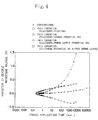
- Figure 4 illustrates variations in reverse withstand voltage with the passage of stress time where mutually different voltages are applied to the electrode 17 in the semiconductor device of the present invention. For the purpose of comparison, data about a conventional semiconductor device is also illustrated in Figure 4 .
- the electrode 17 is biased at a power supply potential of 5 V, for example, then the variation in reverse withstand voltage with time can be suppressed at about 0.3 V even after stress has been applied for 1,000 seconds.
- the variation in reverse withstand voltage can be suppressed within about +0.3 V in the same way as allowing the electrode 17 to be floating.
- the electrode 17 is biased at a potential equal to that of the N-type doped layer 15 , the variation in reverse withstand voltage can be suppressed within about -0.35 V, although the reverse withstand voltage decreases in this case.
- the electrode 17 surrounds the active region 13 .
- the electrode 17 does not have to entirely surround the active region 13 .
- the rate of increase/decrease in field strength decelerates because of the above-described mechanism in the portions encircled by the electrode 17 . Accordingly, the variation in reverse withstand voltage with time can be suppressed, too.
- the type of a bias applied to the electrode should be correlated with the specific structure of the semiconductor device in order to attain the effects of the present invention most efficiently.
- the correlation is variable, because the majority carriers trapped in the interface between the field oxide 12 and the P-type doped layer 14 are sometimes holes and sometimes electrons depending on the type of the semiconductor device.
- the electric field in the direction originating from the N-type doped layer 15 toward the P-type semiconductor substrate 11 is weakened at a lower rate in the pn junction, even if the stress is continuously applied for a longer and longer time. Consequently, the variation in reverse withstand voltage with time can be suppressed.
- the electric field in the direction originating from the N-type doped layer 15 toward the P-type semiconductor substrate 11 is strengthened at a lower rate in the pn junction, even if the stress is continuously applied for a longer and longer time. Consequently, the variation in reverse withstand voltage with time can be suppressed.
- the potential applied through the second aluminum interconnect 21 to the electrode 17 i.e., the potential inducing only one of depletion layer, minority carriers and majority carriers on the surface of the P-type semiconductor substrate 11 and the P-type doped layer 14
- the potential applied through the second aluminum interconnect 21 to the electrode 17 also varies with time or with the transition of states because of carrier trapping in the interface between the field oxide 12 and the P-type doped layer 14 . That is to say, a plurality of modes, where depletion layer, minority carriers and majority carriers are respectively induced on the surface of the P-type semiconductor substrate 11 and the P-type doped layer 14 , sometimes coexist in a single semiconductor device. Accordingly, by changing the potential applied to the electrode 17 in accordance with the transition of the modes, the variation in reverse withstand voltage shown in Figure 4 can be suppressed with the range of ⁇ 0.5 V irrespective of the type of the semiconductor device.
- the function of finely regulating the potential of the electrode 17 is not always easily implementable, because such a control requires an overly complicated configuration.
- the function of regulating the potential of the electrode 17 at a ground potential, a power supply potential or the potential of the N-type doped layer 15 is easily implementable, because only electrical connections at respective parts should be controlled to do so. Accordingly, even if various modes, inducing depletion layer, minority carriers and majority carriers on the surface of the P-type semiconductor substrate 11 and the P-type doped layer 14 , coexist in a single semiconductor device, the variation in reverse withstand voltage with time has only to be ultimately suppressed.
- the variation in voltage applied to the N-type doped layer 15 with time can be suppressed at about 0.3, 0.1 and -0.35 V, where the electrode 17 is biased at ground potential, power supply potential and potential of the N-type doped layer 15 , respectively, as shown in Figure 4 .
- the electrode 17 can be easily biased at an arbitrary constant voltage between the ground and power supply potentials by interposing a resistor between a power supply terminal and the electrode 17 .
- the semiconductor device is operated as a clamping diode for a certain period of time by biasing the electrode 17 at the power supply potential, for example, through the aluminum interconnect 21 . And then the electrode 17 is biased at a potential equal to that of the N-type doped layer 15 , thereby releasing the trapped holes.
- the electric field in the direction originating from the N-type doped layer 15 toward the P-type semiconductor substrate 11 in the pn junction, which has once been weakened can be restored into its initial state. Accordingly, the variation in reverse withstand voltage with time can also be suppressed after all. Even when electrons are trapped in the interface between the field oxide 12 and the P-type doped layer 14 , the same refresh principle is applicable for releasing the trapped carriers, although the polarity of the voltage applied to the electrode 17 is opposite in such a case.
- holes, trapped in the interface between the field oxide 12 and the P-type doped layer 14 may be released every cycle by alternately and repeatedly applying power supply potential and potential of the N-type doped layer 15 to the electrode 17 through the second aluminum interconnect 21 .
- the electric field in the direction originating from the N-type doped layer 15 toward the P-type semiconductor substrate 11 in the pn junction, which has once been weakened can be restored into its initial state on a cycle-by-cycle basis. Accordingly, the variation in reverse withstand voltage with time can also be suppressed after all.
- the same refresh principle is applicable for releasing the trapped carriers, although the polarity of the voltage applied to the electrode 17 is opposite in such a case. In short, such a bias as to eliminate carriers trapped should be applied.
- holes, trapped in the interface between the field oxide 12 and the P-type doped layer 14 may be released every cycle by applying power supply potential and potential of the N-type doped layer 15 through the second aluminum interconnect 21 to the electrode 17 like alternating current. That is to say, the potentials should be applied to show positive and negative values cyclically and alternately. In such a case, there is no need to control DC pulses. As a result, the electric field in the direction originating from the N-type doped layer 15 toward the P-type semiconductor substrate 11 in the pn junction, which has once been weakened, can be restored into its initial state on a cycle-by-cycle basis. Accordingly, the variation in reverse withstand voltage with time can also be suppressed after all. If the majority carriers trapped in the interface between the field oxide 12 and the P-type doped layer 14 are electrons, the same refresh principle is applicable for releasing the trapped carriers, although the polarity of the voltage applied to the electrode 17 is opposite in such a case.
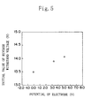
- Figure 5 is a graph illustrating the relationship between the potential of the electrode 17 and the initial value of the reverse withstand voltage. As shown in Figure 5 , if the electrode 17 is biased at the ground potential, the initial value of the reverse withstand voltage is about 13.5 V. However, if the electrode 17 is biased at 3.3 V and 5 V, the initial values of the reverse withstand voltage increase to about 13.8 V and about 14.1 V, respectively. The initial value of the reverse withstand voltage is variable in this manner with the bias applied to the electrode 17 . The reason is believed to be as follows.
- the path of the reverse leakage current flowing through the pn junction between the N-type doped layer 15 and the P-type semiconductor substrate 11 is located near the end of the opening of the field oxide 12 .
- the electrode 17 is biased at the power supply potential, then a depletion layer expands just under the field oxide 12 .
- the path of the reverse leakage current flowing through the pn junction is located deeper than biasing the electrode 17 at the ground potential.
- the semiconductor device of this embodiment can control the path of the leakage current flowing in a reverse biased direction in the pn junction between the N-type doped layer 15 and the P-type semiconductor substrate 11 with the potential of the electrode 17 . As a result, the initial value of the reverse withstand voltage can also be controlled.
- the field oxide 12 is herein formed by a LOCOS technique.
- the field oxide 12 may be replaced with shallow trench isolation (SIT).
- the electrode 17 may be made of any arbitrary conductor other than polysilicon, e.g., aluminum or a multi-layer structure of polysilicon and silicide.
- a single contact hole 19 is formed over the N-type doped layer 15 and over each of the upper, lower, right and left sides of the electrode 17 .
- a plurality of contact holes may be formed at each location.
- the field oxide 12 is formed by a LOCOS technique on the P-type semiconductor substrate 11 so as to surround the regular octagonal active region 13 as shown in Figure 2 .
- an opening is formed in a nitride mask used for formed the LOCOS film.
- P-type dopant ions are implanted at a dose on the order of 10 13 /cm 2 through the opening into the P-type semiconductor substrate 11 , thereby forming the P-type doped layer 14 as a channel stopper to have a dopant concentration on the order of 10 18 /cm 3 .
- the oxide film 16 is formed on the active region 13 surrounded by the field oxide 12 .
- P-type dopant ions are implanted at a dose on the order of 10 12 /cm 2 using the field oxide 12 as a mask, thereby forming the reverse withstand voltage regulating region 25 in substantially the entire active region 13 to have a dopant concentration on the order of 10 17 /cm 2 .
- a polysilicon film is deposited over the entire surface of the substrate and then patterned to form the electrode 17 in the shape of a regular octagonal ring.
- the electrode 17 is formed to overlap the field oxide 12 and the active region 13 .
- the inner peripheral end of the electrode 17 is located to be about 2 ⁇ m inner to the inner peripheral end of the opening of the field oxide 12 .
- N-type dopant ions are implanted into the P-type semiconductor substrate 11 at a dose on the order of 10 15 /cm 2 using the field oxide 12 and the electrode 17 as a mask, thereby forming the N-type doped layer 15 to have a dopant concentration on the order of 10 20 /cm 3 .
- the N-type doped layer 15 is formed to be offset from the field oxide 12 and the P-type doped layer 14 located under the field oxide 12 .
- the interlevel dielectric film 18 is deposited over the entire surface of the substrate and the contact holes 19 reaching the N-type doped layer 15 and the electrode 17 , respectively, are formed in the film 18 .
- an aluminum alloy film 19 is deposited over the contact holes 19 and the interlevel dielectric film 18 and patterned, thereby forming the first and second aluminum interconnects 20 and 21 to be connected to the N-type doped layer 15 and the electrode 17 , respectively.
- the structure of the semiconductor device shown in Figures 1 and 2 can be easily formed by performing these process steps.
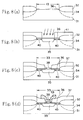
- Figures 6 and 7 are respectively cross-sectional view and plan view of the semiconductor device of the second embodiment.
- the semiconductor device includes: a P-type semiconductor substrate 31 ; a field oxide 32 ; an active region 33 ; a P-type doped layer 34 ; an N-type doped layer 35 ; and a thin oxide film 36 formed over the active region 33 .
- the field oxide 32 is formed by a LOCOS technique on the substrate 31 to surround the active region 33 formed in the shape of regular octagon.
- the P-type doped layer 34 is formed as a channel stopper just under the field oxide 32 by being heavily doped with a P-type dopant.
- the N-type doped layer 35 is formed in the center portion of the active region 33 by being heavily doped with an N-type dopant.
- the inner peripheral end of the field oxide 32 is spaced apart from the N-type doped layer 35 with a predetermined offset region 40 interposed therebetween.
- An interlevel dielectric film 37 is also deposited over the field oxide 32 and the oxide film 36 .
- an aluminum interconnect 39 is formed to make electrical contact with the N-type doped layer 35 though a contact hole 38 formed in the interlevel dielectric film 37 .
- the dopant concentrations in the N-type doped layer 35 and the P-type doped layer 34 are on the orders of 10 20 /cm 3 and 10 1 8 /cm 3 , respectively.
- the active region 33 is shaped like a regular octagon where a pair of opposed sides are spaced from each other by a distance of about 10 ⁇ m to about 40 ⁇ m.
- the gap between the inner peripheral end of the field oxide 32 and the N-type doped layer 35 is about 2 ⁇ m.
- the semiconductor device of this embodiment does not include any member corresponding to the electrode 17 unlike the first embodiment. However, such a structure can also attain the following effects.
- the offset region 40 (about 2 ⁇ m in width) is provided between the field oxide 32 and the N-type doped layer 35 , the N-type doped layer 35 is spaced apart from the P-type doped layer 34 as a channel stopper by the distance of about 2 ⁇ m. Accordingly, the pn junction plane is located about 2 ⁇ m away from the boundary between the active region 33 and the field oxide 32 . Thus, electrons and holes, which have been generated due to the reverse breakdown phenomenon at the pn junction between the N-type doped layer 35 and the P-type semiconductor substrate 31 , are less likely to be trapped in the interface between the field oxide 32 and the P-type doped layer 34 in the vicinity of the boundary between the active region 33 and the field oxide 32 .
- the reverse withstand voltage varies with time substantially in the same way as the case where the electrode 17 of the first embodiment is floating (as represented by the plot identified with ⁇ in Figure 4 ).
- the field oxide 32 is herein formed by a LOCOS technique.
- the field oxide 32 may be replaced with shallow trench isolation (SIT).
- SIT shallow trench isolation
- only a single contact hole 38 is formed over the N-type doped layer 35 .
- a plurality of contact holes may be formed instead.
- the field oxide 32 is formed by a LOCOS technique on the P-type semiconductor substrate 31 so as to surround the regular octagonal active region 33 shown in Figure 7 .
- an opening is formed in a nitride mask used for formed the LOCOS film.
- P-type dopant ions are implanted at a dose on the order of 10 13 /cm 2 through the opening into the P-type semiconductor substrate 31 , thereby forming the P-type doped layer 34 as a channel stopper to have a dopant concentration on the order of 10 18 /cm 3 .
- the oxide film 36 is formed on the active region 33 surrounded by the field oxide 32 .
- the surface of the substrate is coated with a photoresist, which is patterned to form a resist film 41 having a regular octagonal opening.
- the resist film 41 is formed to overlap the field oxide 32 and the active region 33 .
- the inner peripheral end of the opening of the resist film 41 is located to be about 2 ⁇ m inner to the inner peripheral end of the field oxide 32 .
- N-type dopant ions are implanted into the P-type semiconductor substrate 31 at a dose on the order of 10 15 /cm 2 using the resist film 41 as a mask, thereby forming the N-type doped layer 35 to have a dopant concentration on the order of 10 20 /cm 3 .
- the N-type doped layer 35 is formed to be offset from the field oxide 32 and the P-type doped layer 34 located under the field oxide 32 .
- the interlevel dielectric film 37 is deposited over the entire surface of the substrate and the contact hole 38 reaching the N-type doped layer 35 is formed in the film 37 .
- an aluminum alloy film is deposited over the contact hole 38 and the interlevel dielectric film 37 and patterned, thereby forming the aluminum interconnect 39 to be connected to the N-type doped layer 35 .
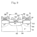
- Figure 9 is a cross-sectional view of the semiconductor device in this embodiment.
- the semiconductor device includes: a P-type semiconductor substrate 51 ; a field oxide 52 ; an active region 53 ; a P-type doped layer 54 ; an N-type doped layer 55 ; and a thin oxide film 56 formed over the active region 53 .
- the field oxide 52 is formed by a LOCOS technique on the substrate 51 to surround the active region 53 formed in the shape of regular octagon.
- the P-type doped layer 54 is formed as a channel stopper just under the field oxide 52 by being heavily doped with a P-type dopant.
- the N-type doped layer 55 is formed in the active region 53 by being heavily doped with an N-type dopant.
- An electrode 57 made of polycrystalline silicon in the shape of regular octagonal ring is provided over the field oxide 52 .
- An interlevel dielectric film 58 is also deposited over the substrate.
- first and second aluminum interconnects 60 and 61 are formed to make electrical contact with the N-type doped layer 55 and the electrode 57 , respectively, though contact holes 59 formed in the interlevel dielectric film 58 .
- the dopant concentrations in the N-type doped layer 55 and the P-type doped layer 54 are on the orders of 10 20 /cm 3 and 10 18 /cm 3 , respectively.
- the active region 53 , or the N-type doped layer 55 is shaped like a regular octagon where a pair of opposed sides are spaced from each other by a distance of about 10 ⁇ m to about 40 ⁇ m.
- the semiconductor device of this embodiment is provided with the electrode 57 on the field oxide 52 , it is possible to suppress carrier trapping in the interface between the field oxide 52 and the P-type doped layer 54 by regulating the voltage applied to the electrode 57 .
- the electrode 57 is biased at a positive potential, then it is harder for the holes to access the interface, resulting in the suppression of hole trapping.
- electron trapping can be suppressed by biasing the electrode 57 at a negative potential.
- the variation in reverse withstand voltage with time can be suppressed within a range of ⁇ 0.5 V, for example, by controlling the voltage applied to the electrode 57 , i.e., selectively applying a bias voltage equal to the ground potential or the power supply potential to the electrode 57 .
- a refresh function for eliminating such trapped carriers may be additionally provided.
Landscapes
- Insulated Gate Type Field-Effect Transistor (AREA)
- Element Separation (AREA)
- Electrodes Of Semiconductors (AREA)
Applications Claiming Priority (2)
| Application Number | Priority Date | Filing Date | Title |
|---|---|---|---|
| JP10742198A JP3472476B2 (ja) | 1998-04-17 | 1998-04-17 | 半導体装置及びその駆動方法 |
| JP10742198 | 1998-04-17 |
Publications (1)
| Publication Number | Publication Date |
|---|---|
| EP0951075A1 true EP0951075A1 (de) | 1999-10-20 |
Family
ID=14458728
Family Applications (1)
| Application Number | Title | Priority Date | Filing Date |
|---|---|---|---|
| EP99102307A Withdrawn EP0951075A1 (de) | 1998-04-17 | 1999-02-05 | Halbleiterbauelement mit p-n Übergang und Methode zu dessen Steuerung |
Country Status (3)
| Country | Link |
|---|---|
| US (2) | US6388308B1 (de) |
| EP (1) | EP0951075A1 (de) |
| JP (1) | JP3472476B2 (de) |
Cited By (4)
| Publication number | Priority date | Publication date | Assignee | Title |
|---|---|---|---|---|
| US6583453B2 (en) | 2000-11-07 | 2003-06-24 | Matsushita Electric Industrial Co., Ltd. | Semiconductor device having a voltage-regulator device |
| EP1355363A3 (de) * | 2002-04-18 | 2007-08-01 | Matsushita Electric Industrial Co., Ltd. | Halbleitervorrichtung und Herstellungsverfahren |
| JP2016009825A (ja) * | 2014-06-26 | 2016-01-18 | 富士通セミコンダクター株式会社 | 半導体装置及びその製造方法 |
| CN112002767A (zh) * | 2020-08-12 | 2020-11-27 | 杰华特微电子(杭州)有限公司 | 齐纳二极管及其制造方法 |
Families Citing this family (7)
| Publication number | Priority date | Publication date | Assignee | Title |
|---|---|---|---|---|
| JP2004214575A (ja) | 2003-01-09 | 2004-07-29 | Matsushita Electric Ind Co Ltd | 半導体装置 |
| US7183626B2 (en) * | 2004-11-17 | 2007-02-27 | International Rectifier Corporation | Passivation structure with voltage equalizing loops |
| DE102010028207A1 (de) * | 2010-04-26 | 2011-10-27 | Robert Bosch Gmbh | Gleichrichter-Brückenschaltung |
| EP2549541B1 (de) * | 2011-07-19 | 2019-10-02 | Elmos Semiconductor Aktiengesellschaft | Festkörper-Diode |
| JP6001309B2 (ja) | 2012-04-17 | 2016-10-05 | エスアイアイ・セミコンダクタ株式会社 | 半導体装置 |
| KR102011174B1 (ko) * | 2012-09-27 | 2019-08-14 | 로무 가부시키가이샤 | 칩 다이오드 및 그 제조 방법 |
| JP2014179650A (ja) * | 2014-05-30 | 2014-09-25 | Toshiba Corp | ダイオード |
Citations (3)
| Publication number | Priority date | Publication date | Assignee | Title |
|---|---|---|---|---|
| US3798512A (en) * | 1970-09-28 | 1974-03-19 | Ibm | Fet device with guard ring and fabrication method therefor |
| EP0091256A2 (de) * | 1982-03-31 | 1983-10-12 | Fujitsu Limited | CMOS-Anordnung |
| EP0204336A2 (de) * | 1985-06-07 | 1986-12-10 | Fujitsu Limited | MISFET-Halbleiteranordnung mit verminderten Leckstrom |
Family Cites Families (13)
| Publication number | Priority date | Publication date | Assignee | Title |
|---|---|---|---|---|
| FR2623018B1 (fr) * | 1987-11-06 | 1990-02-09 | Thomson Semiconducteurs | Circuit integre protege contre les decharges electrostatiques avec seuil de protection variable |
| JPH0314231A (ja) | 1989-06-13 | 1991-01-22 | Toshiba Corp | 半導体リミッタ及びその製造方法 |
| JPH04145673A (ja) | 1990-10-08 | 1992-05-19 | Nec Corp | 積層セラミック圧電素子 |
| JP3028585B2 (ja) | 1990-10-25 | 2000-04-04 | 日本電気株式会社 | 磁気抵抗効果素子 |
| JPH04162681A (ja) | 1990-10-26 | 1992-06-08 | Nec Corp | 半導体装置 |
| JPH04245673A (ja) | 1991-01-31 | 1992-09-02 | Matsushita Electron Corp | 半導体内部昇圧装置 |
| JPH04262580A (ja) | 1991-02-18 | 1992-09-17 | Nec Corp | 半導体装置 |
| WO1993019490A1 (fr) * | 1992-03-23 | 1993-09-30 | Rohm Co., Ltd. | Diode de regulation de tension |
| JP3014231B2 (ja) | 1992-12-01 | 2000-02-28 | 鐘紡株式会社 | 有機リン化合物の製造方法 |
| DE4343365A1 (de) * | 1993-12-18 | 1995-07-13 | Bosch Gmbh Robert | Driftfreie Lawinendurchbruchdiode |
| JP3332545B2 (ja) | 1994-01-28 | 2002-10-07 | 三洋電機株式会社 | 半導体装置及びその製造方法 |
| JPH08288459A (ja) | 1995-04-10 | 1996-11-01 | Matsushita Electron Corp | 半導体抵抗素子 |
| JP3412393B2 (ja) | 1996-04-19 | 2003-06-03 | 松下電器産業株式会社 | 半導体装置 |
-
1998
- 1998-04-17 JP JP10742198A patent/JP3472476B2/ja not_active Expired - Fee Related
-
1999
- 1999-01-29 US US09/239,949 patent/US6388308B1/en not_active Expired - Fee Related
- 1999-02-05 EP EP99102307A patent/EP0951075A1/de not_active Withdrawn
-
2002
- 2002-02-22 US US10/079,510 patent/US6686641B2/en not_active Expired - Lifetime
Patent Citations (3)
| Publication number | Priority date | Publication date | Assignee | Title |
|---|---|---|---|---|
| US3798512A (en) * | 1970-09-28 | 1974-03-19 | Ibm | Fet device with guard ring and fabrication method therefor |
| EP0091256A2 (de) * | 1982-03-31 | 1983-10-12 | Fujitsu Limited | CMOS-Anordnung |
| EP0204336A2 (de) * | 1985-06-07 | 1986-12-10 | Fujitsu Limited | MISFET-Halbleiteranordnung mit verminderten Leckstrom |
Non-Patent Citations (2)
| Title |
|---|
| OHYU K ET AL: "FEASIBILITY OF HIGH-ENERGY BORON IMPLANTATION FOR P-TYPE RETROGRADEWELL FORMATION", NUCLEAR INSTRUMENTS & METHODS IN PHYSICS RESEARCH, SECTION - B: BEAM INTERACTIONS WITH MATERIALS AND ATOMS, vol. B37/38, no. 2, 2 February 1989 (1989-02-02), pages 749 - 752, XP000104757 * |
| VANSTRAELEN G ET AL: "GENERATION LIFETIME MONITORING ON HIGH RESISTIVITY SILICON USING GATED DIODES", NUCLEAR INSTRUMENTS & METHODS IN PHYSICS RESEARCH, SECTION - A: ACCELERATORS, SPECTROMETERS, DETECTORS AND ASSOCIATED EQUIPMENT, vol. A288, no. 1, 1 March 1990 (1990-03-01), pages 48 - 53, XP000100322 * |
Cited By (4)
| Publication number | Priority date | Publication date | Assignee | Title |
|---|---|---|---|---|
| US6583453B2 (en) | 2000-11-07 | 2003-06-24 | Matsushita Electric Industrial Co., Ltd. | Semiconductor device having a voltage-regulator device |
| EP1355363A3 (de) * | 2002-04-18 | 2007-08-01 | Matsushita Electric Industrial Co., Ltd. | Halbleitervorrichtung und Herstellungsverfahren |
| JP2016009825A (ja) * | 2014-06-26 | 2016-01-18 | 富士通セミコンダクター株式会社 | 半導体装置及びその製造方法 |
| CN112002767A (zh) * | 2020-08-12 | 2020-11-27 | 杰华特微电子(杭州)有限公司 | 齐纳二极管及其制造方法 |
Also Published As
| Publication number | Publication date |
|---|---|
| JPH11307787A (ja) | 1999-11-05 |
| JP3472476B2 (ja) | 2003-12-02 |
| US6388308B1 (en) | 2002-05-14 |
| US20020098615A1 (en) | 2002-07-25 |
| US6686641B2 (en) | 2004-02-03 |
Similar Documents
| Publication | Publication Date | Title |
|---|---|---|
| US9583603B2 (en) | ESD protection with integrated LDMOS triggering junction | |
| KR100638456B1 (ko) | 이에스디 보호회로 및 그 제조방법 | |
| KR100220385B1 (ko) | 정전기 보호 소자 | |
| US9786657B1 (en) | Semiconductor structure including a transistor including a gate electrode region provided in a substrate and method for the formation thereof | |
| KR100447824B1 (ko) | 기생 용량을 증가시키지 않으면서 항복 전압이 임의의값으로 설정될 수 있는 다이오드와 그 제조 방법 | |
| JP3173268B2 (ja) | Mis電界効果トランジスタを備えた半導体装置 | |
| JP2004519862A (ja) | 電界効果トランジスタの構造体及び製造方法 | |
| US6686641B2 (en) | Semiconductor device and method for driving the same | |
| US6670685B2 (en) | Method of manufacturing and structure of semiconductor device with floating ring structure | |
| US10312284B2 (en) | Semiconductor device and semiconductor device manufacturing method | |
| US5440165A (en) | Semiconductor device with means for suppressing electric fields | |
| US6914270B2 (en) | IGBT with PN insulation and production method | |
| TW201419489A (zh) | 靜電放電裝置及其製造方法 | |
| CN100423256C (zh) | 半导体集成电路中的静电放电保护电路 | |
| US5221635A (en) | Method of making a field-effect transistor | |
| TWI278095B (en) | High voltage operating electrostatic discharge protection device | |
| US6207996B1 (en) | Semiconductor device and method for manufacturing the same | |
| US6677208B2 (en) | Transistor with bottomwall/sidewall junction capacitance reduction region and method | |
| JPH08195443A (ja) | 半導体装置及びその製造方法 | |
| US7968415B2 (en) | Transistor with reduced short channel effects and method | |
| US6900504B2 (en) | Integrated structure effective to form a MOS component in a dielectrically insulated well | |
| JP2004214575A (ja) | 半導体装置 | |
| JP3943322B2 (ja) | 半導体装置 | |
| US5416339A (en) | Semiconductor device having electrode for collecting electric charge in channel region | |
| JPH0652738B2 (ja) | 絶縁ゲ−ト型電界効果トランジスタ |
Legal Events
| Date | Code | Title | Description |
|---|---|---|---|
| PUAI | Public reference made under article 153(3) epc to a published international application that has entered the european phase |
Free format text: ORIGINAL CODE: 0009012 |
|
| AK | Designated contracting states |
Kind code of ref document: A1 Designated state(s): DE FR GB NL |
|
| AX | Request for extension of the european patent |
Free format text: AL;LT;LV;MK;RO;SI |
|
| 17P | Request for examination filed |
Effective date: 19991202 |
|
| AKX | Designation fees paid |
Free format text: DE FR GB NL |
|
| RAP1 | Party data changed (applicant data changed or rights of an application transferred) |
Owner name: MATSUSHITA ELECTRIC INDUSTRIAL CO., LTD. |
|
| 17Q | First examination report despatched |
Effective date: 20060926 |
|
| STAA | Information on the status of an ep patent application or granted ep patent |
Free format text: STATUS: THE APPLICATION HAS BEEN WITHDRAWN |
|
| 18W | Application withdrawn |
Effective date: 20080414 |