EP0090633A2 - Halbleiteranordnung mit Kühler - Google Patents
Halbleiteranordnung mit Kühler Download PDFInfo
- Publication number
- EP0090633A2 EP0090633A2 EP83301736A EP83301736A EP0090633A2 EP 0090633 A2 EP0090633 A2 EP 0090633A2 EP 83301736 A EP83301736 A EP 83301736A EP 83301736 A EP83301736 A EP 83301736A EP 0090633 A2 EP0090633 A2 EP 0090633A2
- Authority
- EP
- European Patent Office
- Prior art keywords
- pillar
- radiator
- semiconductor device
- hole
- semiconductor
- Prior art date
- Legal status (The legal status is an assumption and is not a legal conclusion. Google has not performed a legal analysis and makes no representation as to the accuracy of the status listed.)
- Granted
Links
Images


Classifications
-
- H10W40/22—
-
- H10W72/884—
Definitions
- the present invention relates to a semiconductor device. More particularly, it relates to an improvement in a radiator for cooling a semiconductor chip which generates a large amount of heat.
- a radiator is attached to a semiconductor integrated-circuit (IC) package which houses an IC chip which generates a large amount of heat.
- IC semiconductor integrated-circuit
- Such a radiator comprises a pillar and a plurality of fins disposed on the pillar.
- the pillar is secured to a molded body of plastic or a ceramic body which houses the IC chip.
- the size of the fins corresponds to the.-size of the IC package and is not uniformed.
- a number of semiconductor devices, each of which comprises an IC package and a radiator are densely mounted on a printed circuit board. It is inconvenient to handle such small-sized semiconductor devices, and, also, it is difficult to place them in a predetermined position when mounting them on a printed board.
- An object of the present invention is to provide a semiconductor device having a radiator, the device being easy to handle and thereby rendering the positioning thereof and the replacing thereof easy without degrading the efficiency of the radiation of heat.
- a semiconductor device having a radiator according to the present invention comprises: a semiconductor package which houses a semiconductor chip therein; and a radiator comprising a pillar and a plurality of fins thereon.
- One end of the pillar is bonded to the semiconductor package, and the other end of said pillar has a first hole. The first hole extends into said pillar along the longitudinal direction of the pillar.
- a semiconductor device comprises a semiconductor package 1 and a radiator 2, as is illustrated in Fig. 1.
- the semiconductor package 1 comprises a base body 13 and lead terminals 11.
- a semiconductor chip 12 is housed within a cavity 26 of the base body 13 and is covered by a cap 15 as is shown in Fig. 2.
- the semiconductor chip 12 is connected to printed circuit patterns 27 formed within the base body 13 by wires 14.
- the radiator 2 comprises a cylindrical pillar 3 provided with a plurality of fins 4 thereon.
- the lower end of the pillar 3 is bonded to the base body 13 of the semiconductor package 1 with an adhesive agent 16, such as epoxy resin.
- a hole 5 is formed in the upper end of the pillar 3 and extends along the longitudinal direction of the pillar 3.
- the pillar 3 and the fins 4 are made of aluminium, copper, molybdenum, or the like.
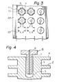
- a vacuum chuck 6, illustrated in Fig. 4 is used to handle the semiconductor device. An access end 7 of the vacuum chuck 6 is inserted into the hole 5.' Vacuum is applied through a vacuum passage 8 so that the semiconductor device is sucked and held by the vacuum chuck 6. The semiconductor device sucked and held by the vacuum chuck 6 is picked up and is conveyed to, for example, a printed circuit board 22, illustrated in Fig. 3.
- the semiconductor device is disposed where pad patterns 23 are formed by placing each lead terminal 11 on a corresponding pad pattern 23. Then the lead terminals 11 are soldered to the pad patterns 23.
- the semiconductor device can be automatically conveyed to and placed in a predetermined position by an automatic positioning machine provided with a vacuum chuck. It is desirable that the diameter of the fins 4 is large enough to cover the base body 13 of the semiconductor package but is less than the width between the ends of the lead terminals on opposite sides of the base body 13. Therefore, positioning of the semiconductor device is easy since the operator can see the lead terminals 11 and the pad patterns 23. When an automatic positioning machine is used, the diameter of the fins 4 may be increased to a degree in which the fins of the adjacent semiconductor devices do not contact each other, thereby enhancing the efficiency of heat radiation. Cooling air is supplied, as is illustrated by the arrows in Fig. 3, to the printed board 22, on which a number of semiconductor devices are mounted. Disc-shaped fins are desirable for decreasing the resistance to the flow of the cooling air. Disc-shaped fins are also desirable from the viewpoint of production.
- a tweezers shaped instrument which has obliquely crossed ends may be used instead of a vacuum chuck to pick up the semiconductor device.
- the ends of the tweezer-shaped instrument is inserted into the hole 5 of the radiator 2. Then the inserted ends of the instrument are opened by hand or by an appropriate spring means so as to push against the inside surface of the hole 5 so that the semiconductor device can be picked up by the instrument.
- the hole 5 it is preferable to form the hole 5 in such a manner that one type of IC package can be distinguished from another according to the depth of the hole 5. If this is done, the type of IC package can be distinguished by the inserted length of the vacuum chuck or by measuring the depth of the hole 5 with an appropriate instrument. Not only does this make it easy for an operator to distinguish an IC package, it also makes possible the automatic distinguishing of an IC package.
- FIG. 5 Another embodiment of the present invention is sectionally illustrated in Fig. 5.
- a metal plate 17 of molybdenum is disposed on the upper surface of the IC package 1.
- a metal stud 18 is bonded onto the metal plate 17 with a soldering agent 19.
- the IC chip 12 is attached to the metal plate 17 through a metal base 21. Therefore, the back surface of the IC chip 12 is electrically connected to the stud 18.
- a hole 5 is formed in the upper end of the pillar 3 of the radiator 2.
- a second hole 9, small in diameter and corresponding to the diameter of the stud 18, is formed in the lower portion of the pillar 3 in series with the hole 5.
- the radiator 2 is attached to the IC package 1 by inserting the stud 18 into the second hole 9 of the radiator 2 and bonding it to the IC package with an adhesive agent 10.
- the hole 5 is convenient not only for picking up the semiconductor device but also for inserting a probe 20 into it so as to make electrical contact with the IC chip 12 through the stud 18.
- the function of the IC chip 12 can be easily tested since power can be supplied to the IC chip 12 through the probe 20 instead of through the lead terminal 11.
- the inventors performed an experiment in which it was confirmed that the hole 5 and the second hole 9 do not affect the efficiency of heat radiation of the radiator.
- the reason of this is that amount of heat to be radiated from the upper portion of the pillar is small since large amount of heat conducted from the IC package is radiated through fins provided on the lower portion of the pillar. That is, amount of heat conducted through the upper portion of the pillar is small while amount of heat conducted through the pillar near the bonding portion between the pillar 3 and the base body 13 is large. Therefore, the efficiency of heat radiation of the radiator provided with a hole on the upper portion of the pillar is not degraded as compared with the radiator without such a hole.
- the type of IC package is not limited to a flat package in which lead terminals are soldered onto the surface of the printed board. Any type of IC package, such as a package in which lead terminals are inserted into through holes of the printed board, may be used.
- the radiator according to the present invention makes it possible to easily handle the semiconductor device and to easily distinguish each IC package.
- an IC package can be easily and precisely placed in a predetermined position.
- an IC package can be automatically positioned. This is especially advantageous when a number of semiconductor devices are to be densely mounted on a printed board.
Landscapes
- Cooling Or The Like Of Semiconductors Or Solid State Devices (AREA)
Applications Claiming Priority (2)
| Application Number | Priority Date | Filing Date | Title |
|---|---|---|---|
| JP57050733A JPS58169943A (ja) | 1982-03-29 | 1982-03-29 | 半導体装置 |
| JP50733/82 | 1982-03-29 |
Publications (3)
| Publication Number | Publication Date |
|---|---|
| EP0090633A2 true EP0090633A2 (de) | 1983-10-05 |
| EP0090633A3 EP0090633A3 (en) | 1985-08-28 |
| EP0090633B1 EP0090633B1 (de) | 1989-07-19 |
Family
ID=12867044
Family Applications (1)
| Application Number | Title | Priority Date | Filing Date |
|---|---|---|---|
| EP83301736A Expired EP0090633B1 (de) | 1982-03-29 | 1983-03-28 | Halbleiteranordnung mit Kühler |
Country Status (5)
| Country | Link |
|---|---|
| US (1) | US4688077A (de) |
| EP (1) | EP0090633B1 (de) |
| JP (1) | JPS58169943A (de) |
| DE (1) | DE3380241D1 (de) |
| IE (1) | IE54726B1 (de) |
Families Citing this family (26)
| Publication number | Priority date | Publication date | Assignee | Title |
|---|---|---|---|---|
| US4878108A (en) * | 1987-06-15 | 1989-10-31 | International Business Machines Corporation | Heat dissipation package for integrated circuits |
| US4887147A (en) * | 1987-07-01 | 1989-12-12 | Digital Equipment Corporation | Thermal package for electronic components |
| US5057903A (en) * | 1989-07-17 | 1991-10-15 | Microelectronics And Computer Technology Corporation | Thermal heat sink encapsulated integrated circuit |
| EP0463758A1 (de) * | 1990-06-22 | 1992-01-02 | Digital Equipment Corporation | Hohlpackung für Chip und Herstellungsverfahren |
| JPH06196587A (ja) * | 1992-12-24 | 1994-07-15 | Toshiba Corp | 半導体装置 |
| JPH076230U (ja) * | 1993-06-29 | 1995-01-27 | 鶴夫 浅野 | 寝間着 |
| US5646826A (en) * | 1995-01-26 | 1997-07-08 | Northern Telecom Limited | Printed circuit board and heat sink arrangement |
| US5764484A (en) * | 1996-11-15 | 1998-06-09 | Olin Corporation | Ground ring for a metal electronic package |
| JP2000500619A (ja) * | 1995-11-20 | 2000-01-18 | オリン コーポレイション | 金属電子パッケージ用の接地リング |
| US6326687B1 (en) | 1998-09-01 | 2001-12-04 | Micron Technology, Inc. | IC package with dual heat spreaders |
| US6633484B1 (en) | 2000-11-20 | 2003-10-14 | Intel Corporation | Heat-dissipating devices, systems, and methods with small footprint |
| WO2002041396A2 (en) * | 2000-11-20 | 2002-05-23 | Intel Corporation | High performance heat sink configurations for use in high density packaging applications |
| US6549411B1 (en) * | 2000-12-20 | 2003-04-15 | Edward Herbert | Flexible heat sinks and method of attaching flexible heat sinks |
| US6479895B1 (en) * | 2001-05-18 | 2002-11-12 | Intel Corporation | High performance air cooled heat sinks used in high density packaging applications |
| US6705144B2 (en) | 2001-09-10 | 2004-03-16 | Intel Corporation | Manufacturing process for a radial fin heat sink |
| US6657862B2 (en) | 2001-09-10 | 2003-12-02 | Intel Corporation | Radial folded fin heat sinks and methods of making and using same |
| US6671172B2 (en) * | 2001-09-10 | 2003-12-30 | Intel Corporation | Electronic assemblies with high capacity curved fin heat sinks |
| US6622786B1 (en) | 2002-04-17 | 2003-09-23 | International Business Machines Corporation | Heat sink structure with pyramidic and base-plate cut-outs |
| CN2676128Y (zh) * | 2003-12-11 | 2005-02-02 | 东莞莫仕连接器有限公司 | 导热装置 |
| DE102007056269A1 (de) * | 2007-10-22 | 2009-04-23 | Rohde & Schwarz Gmbh & Co. Kg | Gekühltes Multichipmodul |
| US7845393B2 (en) * | 2007-11-06 | 2010-12-07 | Jiing Tung Tec. Metal Co., Ltd. | Thermal module |
| TWI389272B (zh) * | 2009-04-22 | 2013-03-11 | 台達電子工業股份有限公司 | 電子元件之散熱模組及其組裝方法 |
| CN102612175A (zh) * | 2012-03-30 | 2012-07-25 | 苏州苏海亚电气有限公司 | 温控加热器 |
| CN102611016A (zh) * | 2012-03-31 | 2012-07-25 | 苏州苏海亚电气有限公司 | 新型加热器 |
| DE102013223461A1 (de) * | 2013-11-18 | 2015-05-21 | Rohde & Schwarz Gmbh & Co. Kg | Kühlkörper zum Abtransport von Wärme |
| GB2598343B (en) * | 2020-08-27 | 2022-11-30 | Continental Automotive Romania Srl | Circular heatsink |
Family Cites Families (11)
| Publication number | Priority date | Publication date | Assignee | Title |
|---|---|---|---|---|
| US2994017A (en) * | 1956-09-07 | 1961-07-25 | Int Rectifier Corp | Air-cooled rectifier assembly |
| NL239393A (de) * | 1957-07-31 | |||
| US3457988A (en) * | 1967-05-15 | 1969-07-29 | Westinghouse Electric Corp | Integral heat sink for semiconductor devices |
| JPS53126276A (en) * | 1977-04-11 | 1978-11-04 | Nippon Telegr & Teleph Corp <Ntt> | Heat dissipation construction of multichip mounting substrate |
| JPS5471572A (en) * | 1977-11-18 | 1979-06-08 | Fujitsu Ltd | Semiconductor device |
| JPS5724021Y2 (de) * | 1978-07-14 | 1982-05-25 | ||
| JPS5561049A (en) * | 1978-10-31 | 1980-05-08 | Furukawa Electric Co Ltd:The | Radiator for semiconductor |
| US4292647A (en) * | 1979-04-06 | 1981-09-29 | Amdahl Corporation | Semiconductor package and electronic array having improved heat dissipation |
| JPS56122149A (en) * | 1980-02-29 | 1981-09-25 | Fujitsu Ltd | Heat dissipating structure for semiconductor device |
| EP0054597A1 (de) * | 1980-12-18 | 1982-06-30 | International Business Machines Corporation | Kühlanordnung für Modul-Steckerstifte |
| DE3278321D1 (en) * | 1981-11-10 | 1988-05-11 | Fujitsu Ltd | Semiconductor devices provided with heat-dissipating means |
-
1982
- 1982-03-29 JP JP57050733A patent/JPS58169943A/ja active Granted
-
1983
- 1983-03-28 DE DE8383301736T patent/DE3380241D1/de not_active Expired
- 1983-03-28 EP EP83301736A patent/EP0090633B1/de not_active Expired
- 1983-03-29 IE IE706/83A patent/IE54726B1/en not_active IP Right Cessation
-
1986
- 1986-01-28 US US06/822,964 patent/US4688077A/en not_active Expired - Fee Related
Also Published As
| Publication number | Publication date |
|---|---|
| JPS6339106B2 (de) | 1988-08-03 |
| IE830706L (en) | 1983-09-29 |
| EP0090633B1 (de) | 1989-07-19 |
| EP0090633A3 (en) | 1985-08-28 |
| DE3380241D1 (en) | 1989-08-24 |
| US4688077A (en) | 1987-08-18 |
| JPS58169943A (ja) | 1983-10-06 |
| IE54726B1 (en) | 1990-01-17 |
Similar Documents
| Publication | Publication Date | Title |
|---|---|---|
| EP0090633A2 (de) | Halbleiteranordnung mit Kühler | |
| US6188127B1 (en) | Semiconductor packing stack module and method of producing the same | |
| US5561594A (en) | Circuit connection in an electrical assembly | |
| US7193329B2 (en) | Semiconductor device | |
| EP0333374B1 (de) | Randmontierte Packung vom Oberflächen-Montierungstyp, für integrierte Halbleiterschaltungsanordnungen | |
| EP0862217A2 (de) | Halbleiteranordnung und Halbleiter-Mehrchipmodul | |
| EP1111738A1 (de) | Halbleitervorrichtung und substrat für eine halbleitervorrichtung | |
| US5461257A (en) | Integrated circuit package with flat-topped heat sink | |
| JPH0376582B2 (de) | ||
| US6191474B1 (en) | Vertically mountable interposer assembly and method | |
| US6750534B2 (en) | Heat spreader hole pin 1 identifier | |
| EP0623954A1 (de) | Vergossene Kunststoffverkapselung für elektronische Anordnungen | |
| EP1335426A2 (de) | Verkapselte Halbleiteranordnung und Herstellungsverfahren dafür | |
| EP0095391B1 (de) | Montierung von leitungslosen Chip-Trägern | |
| JP2801810B2 (ja) | 樹脂封止型半導体装置 | |
| US5665649A (en) | Process for forming a semiconductor device base array and mounting semiconductor devices thereon | |
| EP0167538B1 (de) | Flachgehäuse für scheibchen mit einem integrierten speicherschaltkreis | |
| JPH03238852A (ja) | モールド型半導体集積回路 | |
| JPS60109295A (ja) | 実装基板およびそれを用いた実装体 | |
| KR100216988B1 (ko) | 파워 모듈 | |
| JPH07106486A (ja) | リ−ドフレ−ムとその製造方法、このリ−ドフレ−ムを用いた半導体装置、及び、実装基板 | |
| JP2818700B2 (ja) | 半導体装置 | |
| JPH0497554A (ja) | 高放熱型半導体パッケージ | |
| JPH05243460A (ja) | マルチチップモジュールパッケージ | |
| JPS6276539A (ja) | 電子部品用ソケツト |
Legal Events
| Date | Code | Title | Description |
|---|---|---|---|
| PUAI | Public reference made under article 153(3) epc to a published international application that has entered the european phase |
Free format text: ORIGINAL CODE: 0009012 |
|
| AK | Designated contracting states |
Designated state(s): DE FR GB |
|
| PUAL | Search report despatched |
Free format text: ORIGINAL CODE: 0009013 |
|
| AK | Designated contracting states |
Designated state(s): DE FR GB |
|
| 17P | Request for examination filed |
Effective date: 19860217 |
|
| 17Q | First examination report despatched |
Effective date: 19870731 |
|
| GRAA | (expected) grant |
Free format text: ORIGINAL CODE: 0009210 |
|
| AK | Designated contracting states |
Kind code of ref document: B1 Designated state(s): DE FR GB |
|
| REF | Corresponds to: |
Ref document number: 3380241 Country of ref document: DE Date of ref document: 19890824 |
|
| ET | Fr: translation filed | ||
| RIN2 | Information on inventor provided after grant (corrected) |
Free format text: WAKABAYASHI, TETSUSHI * SUGIMOTO, MASAHIRO * MURATAKE, KIYOSHI |
|
| PLBE | No opposition filed within time limit |
Free format text: ORIGINAL CODE: 0009261 |
|
| STAA | Information on the status of an ep patent application or granted ep patent |
Free format text: STATUS: NO OPPOSITION FILED WITHIN TIME LIMIT |
|
| 26N | No opposition filed | ||
| PGFP | Annual fee paid to national office [announced via postgrant information from national office to epo] |
Ref country code: FR Payment date: 19950309 Year of fee payment: 13 |
|
| PGFP | Annual fee paid to national office [announced via postgrant information from national office to epo] |
Ref country code: GB Payment date: 19960319 Year of fee payment: 14 |
|
| PGFP | Annual fee paid to national office [announced via postgrant information from national office to epo] |
Ref country code: DE Payment date: 19960328 Year of fee payment: 14 |
|
| PG25 | Lapsed in a contracting state [announced via postgrant information from national office to epo] |
Ref country code: FR Effective date: 19961129 |
|
| REG | Reference to a national code |
Ref country code: FR Ref legal event code: ST |
|
| PG25 | Lapsed in a contracting state [announced via postgrant information from national office to epo] |
Ref country code: GB Effective date: 19970328 |
|
| GBPC | Gb: european patent ceased through non-payment of renewal fee |
Effective date: 19970328 |
|
| PG25 | Lapsed in a contracting state [announced via postgrant information from national office to epo] |
Ref country code: DE Effective date: 19971202 |