EP0076942A2 - Verfahren zur Herstellung von integrierten Schaltungsanordnungen mit dielektrischen Isolationszonen - Google Patents
Verfahren zur Herstellung von integrierten Schaltungsanordnungen mit dielektrischen Isolationszonen Download PDFInfo
- Publication number
- EP0076942A2 EP0076942A2 EP82108704A EP82108704A EP0076942A2 EP 0076942 A2 EP0076942 A2 EP 0076942A2 EP 82108704 A EP82108704 A EP 82108704A EP 82108704 A EP82108704 A EP 82108704A EP 0076942 A2 EP0076942 A2 EP 0076942A2
- Authority
- EP
- European Patent Office
- Prior art keywords
- film
- mask pattern
- semiconductor substrate
- polycrystalline silicon
- etched
- Prior art date
- Legal status (The legal status is an assumption and is not a legal conclusion. Google has not performed a legal analysis and makes no representation as to the accuracy of the status listed.)
- Granted
Links
- 238000004519 manufacturing process Methods 0.000 title claims abstract description 8
- 238000002955 isolation Methods 0.000 title description 4
- 239000000758 substrate Substances 0.000 claims abstract description 42
- 239000004065 semiconductor Substances 0.000 claims abstract description 33
- 239000012535 impurity Substances 0.000 claims abstract description 19
- 229910021420 polycrystalline silicon Inorganic materials 0.000 claims description 39
- 238000000034 method Methods 0.000 claims description 32
- 238000005530 etching Methods 0.000 claims description 24
- 229910052581 Si3N4 Inorganic materials 0.000 claims description 5
- HQVNEWCFYHHQES-UHFFFAOYSA-N silicon nitride Chemical compound N12[Si]34N5[Si]62N3[Si]51N64 HQVNEWCFYHHQES-UHFFFAOYSA-N 0.000 claims description 5
- 238000005468 ion implantation Methods 0.000 claims description 2
- 238000001659 ion-beam spectroscopy Methods 0.000 claims description 2
- VYPSYNLAJGMNEJ-UHFFFAOYSA-N Silicium dioxide Chemical compound O=[Si]=O VYPSYNLAJGMNEJ-UHFFFAOYSA-N 0.000 description 34
- 229910052814 silicon oxide Inorganic materials 0.000 description 31
- XUIMIQQOPSSXEZ-UHFFFAOYSA-N Silicon Chemical compound [Si] XUIMIQQOPSSXEZ-UHFFFAOYSA-N 0.000 description 18
- 229910052710 silicon Inorganic materials 0.000 description 18
- 239000010703 silicon Substances 0.000 description 18
- ZOXJGFHDIHLPTG-UHFFFAOYSA-N Boron Chemical compound [B] ZOXJGFHDIHLPTG-UHFFFAOYSA-N 0.000 description 12
- 229910052796 boron Inorganic materials 0.000 description 12
- 238000005229 chemical vapour deposition Methods 0.000 description 6
- 230000003647 oxidation Effects 0.000 description 6
- 238000007254 oxidation reaction Methods 0.000 description 6
- 238000002347 injection Methods 0.000 description 5
- 239000007924 injection Substances 0.000 description 5
- 238000001020 plasma etching Methods 0.000 description 5
- 238000007796 conventional method Methods 0.000 description 4
- 230000002950 deficient Effects 0.000 description 4
- 238000009792 diffusion process Methods 0.000 description 4
- 229920002120 photoresistant polymer Polymers 0.000 description 4
- 229910052782 aluminium Inorganic materials 0.000 description 3
- XAGFODPZIPBFFR-UHFFFAOYSA-N aluminium Chemical compound [Al] XAGFODPZIPBFFR-UHFFFAOYSA-N 0.000 description 3
- 229910000765 intermetallic Inorganic materials 0.000 description 3
- 229910052751 metal Inorganic materials 0.000 description 3
- 239000002184 metal Substances 0.000 description 3
- 229910021332 silicide Inorganic materials 0.000 description 3
- FVBUAEGBCNSCDD-UHFFFAOYSA-N silicide(4-) Chemical compound [Si-4] FVBUAEGBCNSCDD-UHFFFAOYSA-N 0.000 description 3
- 239000000243 solution Substances 0.000 description 3
- 229910052715 tantalum Inorganic materials 0.000 description 3
- GUVRBAGPIYLISA-UHFFFAOYSA-N tantalum atom Chemical compound [Ta] GUVRBAGPIYLISA-UHFFFAOYSA-N 0.000 description 3
- ZOKXTWBITQBERF-UHFFFAOYSA-N Molybdenum Chemical compound [Mo] ZOKXTWBITQBERF-UHFFFAOYSA-N 0.000 description 2
- OAICVXFJPJFONN-UHFFFAOYSA-N Phosphorus Chemical compound [P] OAICVXFJPJFONN-UHFFFAOYSA-N 0.000 description 2
- 238000000137 annealing Methods 0.000 description 2
- 229910052787 antimony Inorganic materials 0.000 description 2
- WATWJIUSRGPENY-UHFFFAOYSA-N antimony atom Chemical compound [Sb] WATWJIUSRGPENY-UHFFFAOYSA-N 0.000 description 2
- 229910052785 arsenic Inorganic materials 0.000 description 2
- RQNWIZPPADIBDY-UHFFFAOYSA-N arsenic atom Chemical compound [As] RQNWIZPPADIBDY-UHFFFAOYSA-N 0.000 description 2
- 229910052681 coesite Inorganic materials 0.000 description 2
- 230000000295 complement effect Effects 0.000 description 2
- 229910052906 cristobalite Inorganic materials 0.000 description 2
- 238000000151 deposition Methods 0.000 description 2
- 239000012212 insulator Substances 0.000 description 2
- 229910052750 molybdenum Inorganic materials 0.000 description 2
- 239000011733 molybdenum Substances 0.000 description 2
- 229910052698 phosphorus Inorganic materials 0.000 description 2
- 239000011574 phosphorus Substances 0.000 description 2
- 238000001259 photo etching Methods 0.000 description 2
- 238000004544 sputter deposition Methods 0.000 description 2
- 229910052682 stishovite Inorganic materials 0.000 description 2
- 229910052905 tridymite Inorganic materials 0.000 description 2
- 238000007740 vapor deposition Methods 0.000 description 2
- 229910001218 Gallium arsenide Inorganic materials 0.000 description 1
- 229910021417 amorphous silicon Inorganic materials 0.000 description 1
- 230000015572 biosynthetic process Effects 0.000 description 1
- 230000015556 catabolic process Effects 0.000 description 1
- 150000001875 compounds Chemical class 0.000 description 1
- 230000008021 deposition Effects 0.000 description 1
- 230000000694 effects Effects 0.000 description 1
- 150000002500 ions Chemical class 0.000 description 1
- 239000000463 material Substances 0.000 description 1
- 229910044991 metal oxide Inorganic materials 0.000 description 1
- 150000004706 metal oxides Chemical class 0.000 description 1
- 230000003071 parasitic effect Effects 0.000 description 1
- 239000002245 particle Substances 0.000 description 1
- 238000000206 photolithography Methods 0.000 description 1
- 239000000377 silicon dioxide Substances 0.000 description 1
- WFKWXMTUELFFGS-UHFFFAOYSA-N tungsten Chemical compound [W] WFKWXMTUELFFGS-UHFFFAOYSA-N 0.000 description 1
- 229910052721 tungsten Inorganic materials 0.000 description 1
- 239000010937 tungsten Substances 0.000 description 1
Images


Classifications
-
- H—ELECTRICITY
- H01—ELECTRIC ELEMENTS
- H01L—SEMICONDUCTOR DEVICES NOT COVERED BY CLASS H10
- H01L21/00—Processes or apparatus adapted for the manufacture or treatment of semiconductor or solid state devices or of parts thereof
- H01L21/02—Manufacture or treatment of semiconductor devices or of parts thereof
- H01L21/04—Manufacture or treatment of semiconductor devices or of parts thereof the devices having potential barriers, e.g. a PN junction, depletion layer or carrier concentration layer
- H01L21/18—Manufacture or treatment of semiconductor devices or of parts thereof the devices having potential barriers, e.g. a PN junction, depletion layer or carrier concentration layer the devices having semiconductor bodies comprising elements of Group IV of the Periodic Table or AIIIBV compounds with or without impurities, e.g. doping materials
- H01L21/26—Bombardment with radiation
- H01L21/263—Bombardment with radiation with high-energy radiation
- H01L21/265—Bombardment with radiation with high-energy radiation producing ion implantation
- H01L21/26506—Bombardment with radiation with high-energy radiation producing ion implantation in group IV semiconductors
- H01L21/26513—Bombardment with radiation with high-energy radiation producing ion implantation in group IV semiconductors of electrically active species
- H01L21/2652—Through-implantation
-
- H—ELECTRICITY
- H01—ELECTRIC ELEMENTS
- H01L—SEMICONDUCTOR DEVICES NOT COVERED BY CLASS H10
- H01L21/00—Processes or apparatus adapted for the manufacture or treatment of semiconductor or solid state devices or of parts thereof
- H01L21/70—Manufacture or treatment of devices consisting of a plurality of solid state components formed in or on a common substrate or of parts thereof; Manufacture of integrated circuit devices or of parts thereof
- H01L21/71—Manufacture of specific parts of devices defined in group H01L21/70
- H01L21/76—Making of isolation regions between components
- H01L21/762—Dielectric regions, e.g. EPIC dielectric isolation, LOCOS; Trench refilling techniques, SOI technology, use of channel stoppers
- H01L21/76224—Dielectric regions, e.g. EPIC dielectric isolation, LOCOS; Trench refilling techniques, SOI technology, use of channel stoppers using trench refilling with dielectric materials
-
- H—ELECTRICITY
- H01—ELECTRIC ELEMENTS
- H01L—SEMICONDUCTOR DEVICES NOT COVERED BY CLASS H10
- H01L21/00—Processes or apparatus adapted for the manufacture or treatment of semiconductor or solid state devices or of parts thereof
- H01L21/70—Manufacture or treatment of devices consisting of a plurality of solid state components formed in or on a common substrate or of parts thereof; Manufacture of integrated circuit devices or of parts thereof
- H01L21/77—Manufacture or treatment of devices consisting of a plurality of solid state components or integrated circuits formed in, or on, a common substrate
- H01L21/78—Manufacture or treatment of devices consisting of a plurality of solid state components or integrated circuits formed in, or on, a common substrate with subsequent division of the substrate into plural individual devices
- H01L21/82—Manufacture or treatment of devices consisting of a plurality of solid state components or integrated circuits formed in, or on, a common substrate with subsequent division of the substrate into plural individual devices to produce devices, e.g. integrated circuits, each consisting of a plurality of components
- H01L21/822—Manufacture or treatment of devices consisting of a plurality of solid state components or integrated circuits formed in, or on, a common substrate with subsequent division of the substrate into plural individual devices to produce devices, e.g. integrated circuits, each consisting of a plurality of components the substrate being a semiconductor, using silicon technology
- H01L21/8232—Field-effect technology
- H01L21/8234—MIS technology, i.e. integration processes of field effect transistors of the conductor-insulator-semiconductor type
- H01L21/8238—Complementary field-effect transistors, e.g. CMOS
- H01L21/823878—Complementary field-effect transistors, e.g. CMOS isolation region manufacturing related aspects, e.g. to avoid interaction of isolation region with adjacent structure
-
- Y—GENERAL TAGGING OF NEW TECHNOLOGICAL DEVELOPMENTS; GENERAL TAGGING OF CROSS-SECTIONAL TECHNOLOGIES SPANNING OVER SEVERAL SECTIONS OF THE IPC; TECHNICAL SUBJECTS COVERED BY FORMER USPC CROSS-REFERENCE ART COLLECTIONS [XRACs] AND DIGESTS
- Y10—TECHNICAL SUBJECTS COVERED BY FORMER USPC
- Y10S—TECHNICAL SUBJECTS COVERED BY FORMER USPC CROSS-REFERENCE ART COLLECTIONS [XRACs] AND DIGESTS
- Y10S438/00—Semiconductor device manufacturing: process
- Y10S438/914—Doping
- Y10S438/924—To facilitate selective etching
-
- Y—GENERAL TAGGING OF NEW TECHNOLOGICAL DEVELOPMENTS; GENERAL TAGGING OF CROSS-SECTIONAL TECHNOLOGIES SPANNING OVER SEVERAL SECTIONS OF THE IPC; TECHNICAL SUBJECTS COVERED BY FORMER USPC CROSS-REFERENCE ART COLLECTIONS [XRACs] AND DIGESTS
- Y10—TECHNICAL SUBJECTS COVERED BY FORMER USPC
- Y10S—TECHNICAL SUBJECTS COVERED BY FORMER USPC CROSS-REFERENCE ART COLLECTIONS [XRACs] AND DIGESTS
- Y10S438/00—Semiconductor device manufacturing: process
- Y10S438/978—Semiconductor device manufacturing: process forming tapered edges on substrate or adjacent layers
Definitions
- the present invention relates to a method of manufacturing a semiconductor device and, more particularly, to a method suitably adapted for forming an isolation region between a well region and a semiconductor substrate of a complementary semiconductor device.
- CMOS Complementary MOS
- MOS Metal Oxide Semiconductor
- a bipolar transistor among various bipolar devices has an npn transistor and a pnp transistor.
- impurity region generally a well region
- the transistors are isolated at the boundary between the well region and the semiconductor substrate.
- CMOS transistor since the p- and n-channel transistors are present on a single semiconductor substrate, defective modes are caused such as the turn-on phenomenon of a parasitic thyristor (so-called latch-up phenomenon) or various breakdown phenomena. In order to prevent such defective modes, possible reduction in the clearance between the p- and n-channel transistors is greatly limited. As a result of this, the clearance margin must be made relatively large.
- a conventional method for forming such an insulating film typically comprises the step of ion-implanting an impurity of the opposite conductivity type to that of a semiconductor substrate into a desired region thereof by the photoetching process (PEP), and diffusing the ion-implanted impurity by annealing to a predetermined depth (e.g., 5 pm), thereby forming a well region in the semiconductor substrate; and forming an insulating film in a boundary region between the well region and the semiconductor substrate by PEP again.
- PEP photoetching process
- a method of manufacturing a semiconductor device comprising the steps of: forming a mask pattern on one major surface of a semiconductor substrate, the mask pattern having side surfaces which are perpendicular to the one major surface or are reversely tapered; ion-implanting an impurity of an opposite conductivity type to that of the semiconductor substrate using the mask pattern; and forming a groove in a portion of the semiconductor substrate which is close to the side surfaces of the mask pattern.
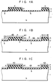
- a p-type region (well region) is formed in an n-type silicon substrate.
- an insulating film such as a silicon oxide film 2 is formed on an n-type silicon substrate 1 by thermal oxidation or the like.
- the insulating film may comprise a silicon nitride film or the like.
- a film such as a polycrystalline silicon film 3 is formed on the entire surface of the silicon oxide film 2.
- the film 3 may alternatively comprise silicon nitride; a metal such as aluminum, molybdenum or tantalum; an intermetallic compound such as a silicide; and the like.
- a photoresist film is formed by a known photolithographic process on a desired portion (a region excluding a prospective p-type well region) of the surface of the polycrystalline silicon film 3.
- the polycrystalline silicon film 3 is etched by a known etching technique such as anisotropic reactive ion etching using the photoresist film as a mask.
- a pattern of the polycrystalline silicon film 3 is formed which has vertical or reversely tapered side walls.
- An insulating film such as a silicon oxide film 4 is formed on the surface of the pattern of the polycrystalline silicon film 3.
- the thickness of the silicon oxide film 4 is smaller than that of the silicon oxide film 2.
- the silicon oxide film 4 may be formed by thermal oxidation or by the CVD (Chemical Vapor Deposition) process.
- a p-type impurity e.g., phosphorus, antimony, or arsenic
- a silicon film such as a polycrystalline silicon film 6 is formed by a known film forming method (e.g., the CVD process, sputtering, or vapor deposition).
- the film 6 may alternatively comprise amorphous silicon.
- the conditions for forming the polycrystalline silicon film 6 are such that polycrystalline silicon is deposited on at least a region, excluding regions 4a, of the silicon oxide film 4 which are on the side surfaces of the polycrystalline silicon film 3.
- Boron of a high concentration (5 x 10 19 cm -3 or higher) is ion-implanted on the entire surface or part thereof (that is, on regions 6b, excluding regions 6a, on the side surfaces of the pattern of the polycrystalline silicon film 3) of the polycrystalline silicon film 6.
- the regions 6a at the side surfaces of the pattern of the polycrystalline silicon film 3 preferably have a boron concentration of about 1 x 10 19 cm-3 or lower, and the regions 6b, excluding the regions 6a, preferably have a boron concentration of about 5 x 10 19 cm -3
- boron is preferably ion-implanted perpendicularly to the silicon substrate 1. Boron is selected in relation to KOH etching to be described later. Therefore, other ions may be selected if other etching solutions are selected.
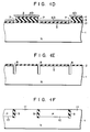
- the polycrystalline silicon film 6 is etched using an etching solution containing KOH. Since the regions 6a having a lower boron concentration are etched faster than the regions 6b of higher boron concentration, the regions 4a on the side surfaces of the silicon oxide film 4 are exposed entirely or in part, as shown in Fig. 1C. Subsequently, the regions 4a on the side surfaces of the silicon oxide film 4 are etched. As shown in Fig. 1D, when the regions 4a on the side surfaces of the silicon oxide film 4 are etched, an opening 7 is formed between the side surfaces of the pattern of the polycrystalline silicon film 3 and the regions 6b of the polycrystalline silicon film 6. The silicon oxide film 2 exposed through the opening 7 is etched until part of the silicon substrate 1 is exposed.
- the polycrystalline silicon film 6, the silicon oxide film 4 and the polycrystalline silicon film 3 are sequentially etched.
- the polycrystalline silicon film 3 is etched by anisotropic etching such as reactive ion etching.
- the silicon substrate 1 is also etched to form an etching groove 8.
- the surface of the silicon substrate 1 excluding the etching groove 8 is covered with the silicon oxide film 2.
- the etching groove 8 is further etched to a desired depth or a depth of the prospective p-type well region.
- an insulating film 9 is formed in the etching groove 8.
- the insulating film 9 may be formed by burying a silicon oxide film within the etching groove 8 by thermal oxidation.
- an insulator such as SiO 2 or SiN may be buried in the etching groove 8 by the CVD process.
- the impurity (boron) in the impurity injection layer 5 is then thermally diffused to form a p-type well region 10.
- the p-type well region 10 and an n-type region 11 are isolated by the insulating film 9.
- An n-channel MOS transistor is formed on the p-type well region 10 and a p-channel MOS transistor is formed on the n-type region 11 according to the conventional CMOS process, to complete a CMOS device.
- a p-type well region is formed in an n-type substrate.
- an n-type well region may alternatively be formed in a p-type substrate.
- annealing may be performed to activate the ion-implanted boron.
- a thin insulating film may be formed on the surface of the polycrystalline silicon film 6.
- the dose of boron may be freely selected such that the concentration of the polycrystalline silicon film 6 may not exceed about 5 x 10 19 c m - 3
- the insulating film 9 may be formed at any position between the n-type region 11 and the p-type well region 10 of the silicon substrate 1 by a single photoetching step and in self-alignment. For this reason, mask misalignment as is encountered with the conventional method need not be considered in circuit designing, and the distance between the p- and n-channel transistors may be reduced, resulting in higher micronization.
- the first embodiment of the present invention also prevents the defective modes of the CMOSs such as the latch-up phenomenon. After the insulating film 9 is formed, thermal diffusion of the impurity in the impurity injection layer 5 is performed. Therefore, lateral diffusion of the impurity may be prevented. Moreover, the width, depth, and shape of the insulating film 9 may be freely selected.
- a p-type well region is formed in an n-type silicon substrate as in the case of the first embodiment.
- an insulating film such as a silicon oxide film 102 is formed on an n-type silicon substrate 101 by thermal oxidation.
- a film such as a polycrystalline silicon film 103 is formed on the entire surface of the silicon oxide film 102.
- the film 103 may alternatively comprise silicon nitride; a metal such as aluminum or tantalum; or an intermetallic compound such as a silicide.
- a photoresist film is formed by photolithography on a desired portion (a region excluding the prospective p-type well region) of the surface of the polycrystalline silicon film 103.
- the polycrystalline silicon film 103 is etched by a known etching technique such as anisotropic reactive ion etching to form a pattern of the polycrystalline silicon film 103.
- An insulating film such as a silicon oxide film 104 is formed on the surface of the polycrystalline silicon film 103.
- the thickness of the silicon oxide film 104 is selected to be smaller than that of the silicon oxide film 102.
- the silicon oxide film 104 may be formed by thermal oxidation or by the CVD process.
- a p-type impurity e.g., phosphorus, antimony or arsenic
- a film such as a polycrystalline silicon film 106 is formed by an anisotropic film forming method (a film deposition method wherein particles are vertically bombarded against the silicon substrate 101 to be deposited thereon, such as sputtering, vapor deposition; the preferred method is ion beam sputtering which provides good linearity).
- the film 106 must comprise a material which may serve as a mask for etching the silicon oxide films 102 and 104 and may therefore alternatively comprise silicon nitride; a metal such as molybdenum, tungsten, tantalum or aluminum; or an intermetallic compound such as a silicide.
- the conditions for forming the polycrystalline silicon film 106 are such that it may not be formed on the entire or on any part of regions 104a of the silicon oxide film 104. If the area where the polycrystalline silicon film 106 is not deposited is too small, the polycrystalline silicon film 106 is etched by a known etching technique (e.g., a wet method using an etching solution, or an isotropic plasma etching method).
- a known etching technique e.g., a wet method using an etching solution, or an isotropic plasma etching method.
- the regions 104a of the silicon oxide film 104 are etched by a known etching technique. Using the etched part as a window, the silicon oxide film 102 below the regions 104a is etched. Subsequently, the polycrystalline silicon film 106 and the silicon oxide film 104 covered thereby are etched. In this state, the surface of the silicon substrate 101 is covered with the silicon oxide film 102 except for regions 107 in the vicinities of the ends of the pattern of the polycrystalline silicon film 103. Thereafter, as shown in Fig. 2D, after the polycrystalline silicon film 103 is etched, the silicon substrate 101 is etched by anisotropic reactive ion etching to form an etching groove 108 of a desired depth.
- an insulating layer 109 is formed in the etching groove 108.
- the insulating film 109 may be formed by forming a silicon oxide film within the etching groove 108 by thermal oxidation.
- the insulating film 109 may also be formed by burying an insulator such as Si0 2 or SiN by the CVD process. After the surface of the silicon substrate 101 is smoothed and the entire surface thereof is exposed, the impurity in the impurity injection layer 105 is thermally diffused to form a p-type well region 110.
- the p-type well region 110 and an n-type region 111 in the silicon substrate 101 are isolated by the insulating layer 109.
- the CMOS device is the completed by the conventional method.
- the polycrystalline silicon film 6 of a uniform thickness is formed on the top and side surfaces of the silicon oxide film 4, and the polycrystalline silicon film 6 on the side surfaces of the silicon oxide film 4 is thereafter etched.
- the polycrystalline silicon film 106 is deposited only in the vertical direction by anisotropic deposition. Therefore, the polycrystalline silicon film 106 is not deposited on the side surfaces of the silicon oxide film 104 from the beginning. Except in this feature, the second embodiment is the same as the first embodiment, and similar effects may be obtained.
- the present invention is not limited to this.
- the present invention may be similarly applied to a bipolar structure comprising an npn transistor and a pnp transistor.
- the semiconductor substrate may comprise a substrate of a III - V group compound such as GaAs in place of the silicon substrate.
Landscapes
- Engineering & Computer Science (AREA)
- Physics & Mathematics (AREA)
- Microelectronics & Electronic Packaging (AREA)
- General Physics & Mathematics (AREA)
- Manufacturing & Machinery (AREA)
- Computer Hardware Design (AREA)
- Condensed Matter Physics & Semiconductors (AREA)
- Power Engineering (AREA)
- High Energy & Nuclear Physics (AREA)
- Health & Medical Sciences (AREA)
- Toxicology (AREA)
- Element Separation (AREA)
- Metal-Oxide And Bipolar Metal-Oxide Semiconductor Integrated Circuits (AREA)
- Drying Of Semiconductors (AREA)
- Local Oxidation Of Silicon (AREA)
Applications Claiming Priority (2)
| Application Number | Priority Date | Filing Date | Title |
|---|---|---|---|
| JP162813/81 | 1981-10-14 | ||
| JP56162813A JPS5864044A (ja) | 1981-10-14 | 1981-10-14 | 半導体装置の製造方法 |
Publications (3)
| Publication Number | Publication Date |
|---|---|
| EP0076942A2 true EP0076942A2 (de) | 1983-04-20 |
| EP0076942A3 EP0076942A3 (en) | 1986-04-16 |
| EP0076942B1 EP0076942B1 (de) | 1989-03-01 |
Family
ID=15761706
Family Applications (1)
| Application Number | Title | Priority Date | Filing Date |
|---|---|---|---|
| EP82108704A Expired EP0076942B1 (de) | 1981-10-14 | 1982-09-21 | Verfahren zur Herstellung von integrierten Schaltungsanordnungen mit dielektrischen Isolationszonen |
Country Status (4)
| Country | Link |
|---|---|
| US (1) | US4463493A (de) |
| EP (1) | EP0076942B1 (de) |
| JP (1) | JPS5864044A (de) |
| DE (1) | DE3279494D1 (de) |
Cited By (10)
| Publication number | Priority date | Publication date | Assignee | Title |
|---|---|---|---|---|
| EP0082256A2 (de) * | 1981-12-10 | 1983-06-29 | Kabushiki Kaisha Toshiba | Verfahren zur Herstellung von Halbleiteranordnungen mit dielektrischen Isolationszonen |
| EP0113517A2 (de) * | 1982-11-29 | 1984-07-18 | Fujitsu Limited | Verfahren zur Herstellung einer Isolationszone |
| EP0097326B1 (de) * | 1982-06-18 | 1987-01-28 | Hitachi, Ltd. | Halbleiteranordnung mit Wannenstruktur |
| US4717689A (en) * | 1984-09-18 | 1988-01-05 | U.S. Philips Corporation | Method of forming semimicron grooves in semiconductor material |
| US4791073A (en) * | 1987-11-17 | 1988-12-13 | Motorola Inc. | Trench isolation method for semiconductor devices |
| EP0391479A2 (de) * | 1989-04-05 | 1990-10-10 | Koninklijke Philips Electronics N.V. | Ein herstellungsverfahren eines bipolaren Transistors |
| EP0391480A2 (de) * | 1989-04-05 | 1990-10-10 | Koninklijke Philips Electronics N.V. | Herstellungsverfahren eines bipolaren Transistors |
| EP0503666A2 (de) * | 1991-03-15 | 1992-09-16 | Sony Corporation | CCD Festkörper-Bildaufnahmevorrichtung |
| US5696020A (en) * | 1994-11-23 | 1997-12-09 | Electronics And Telecommunications Research Institute | Method for fabricating semiconductor device isolation region using a trench mask |
| US5874347A (en) * | 1994-11-23 | 1999-02-23 | Electronics And Telecommunications Research Institute | Method for fabricating field oxide isolation region for semiconductor devices |
Families Citing this family (23)
| Publication number | Priority date | Publication date | Assignee | Title |
|---|---|---|---|---|
| JPS5978542A (ja) * | 1982-10-27 | 1984-05-07 | Nippon Telegr & Teleph Corp <Ntt> | 半導体装置の製造方法 |
| JPS6038861A (ja) * | 1983-08-12 | 1985-02-28 | Hitachi Ltd | 相補型の半導体集積回路装置の製造方法 |
| KR900001267B1 (ko) * | 1983-11-30 | 1990-03-05 | 후지쓰 가부시끼가이샤 | Soi형 반도체 장치의 제조방법 |
| GB8406432D0 (en) * | 1984-03-12 | 1984-04-18 | British Telecomm | Semiconductor devices |
| JPS618945A (ja) * | 1984-06-25 | 1986-01-16 | Nec Corp | 半導体集積回路装置 |
| US4597164A (en) * | 1984-08-31 | 1986-07-01 | Texas Instruments Incorporated | Trench isolation process for integrated circuit devices |
| US4574469A (en) * | 1984-09-14 | 1986-03-11 | Motorola, Inc. | Process for self-aligned buried layer, channel-stop, and isolation |
| US4583282A (en) * | 1984-09-14 | 1986-04-22 | Motorola, Inc. | Process for self-aligned buried layer, field guard, and isolation |
| US4578128A (en) * | 1984-12-03 | 1986-03-25 | Ncr Corporation | Process for forming retrograde dopant distributions utilizing simultaneous outdiffusion of dopants |
| JPS61194767A (ja) * | 1985-02-22 | 1986-08-29 | Nec Corp | 相補型mos半導体装置の製造方法 |
| US5450053A (en) * | 1985-09-30 | 1995-09-12 | Honeywell Inc. | Use of vanadium oxide in microbolometer sensors |
| US4704849A (en) * | 1985-12-17 | 1987-11-10 | Gilbert Zachary R | Wheel-mounted weed trimmer |
| US5300915A (en) * | 1986-07-16 | 1994-04-05 | Honeywell Inc. | Thermal sensor |
| IT1213457B (it) * | 1986-07-23 | 1989-12-20 | Catania A | Procedimento per la fabbricazione di dispositivi integrati, in particolare dispositivi cmos adoppia sacca. |
| FR2610141B1 (fr) * | 1987-01-26 | 1990-01-19 | Commissariat Energie Atomique | Circuit integre cmos et procede de fabrication de zones d'isolation electrique dans ce circuit |
| JPS63193562A (ja) * | 1987-02-06 | 1988-08-10 | Toshiba Corp | バイポ−ラトランジスタの製造方法 |
| US4799990A (en) * | 1987-04-30 | 1989-01-24 | Ibm Corporation | Method of self-aligning a trench isolation structure to an implanted well region |
| US4876214A (en) * | 1988-06-02 | 1989-10-24 | Tektronix, Inc. | Method for fabricating an isolation region in a semiconductor substrate |
| US5286976A (en) * | 1988-11-07 | 1994-02-15 | Honeywell Inc. | Microstructure design for high IR sensitivity |
| KR19980034610A (ko) * | 1996-11-08 | 1998-08-05 | 문정환 | 반도체장치의 소자격리방법 |
| US5989963A (en) * | 1997-07-21 | 1999-11-23 | Advanced Micro Devices, Inc. | Method for obtaining a steep retrograde channel profile |
| US6245649B1 (en) | 1999-02-17 | 2001-06-12 | Advanced Micro Devices, Inc. | Method for forming a retrograde impurity profile |
| CN117174583B (zh) * | 2023-11-02 | 2024-01-30 | 合肥晶合集成电路股份有限公司 | 半导体结构及其制备方法 |
Citations (7)
| Publication number | Priority date | Publication date | Assignee | Title |
|---|---|---|---|---|
| FR1473788A (fr) * | 1965-04-07 | 1967-03-17 | Centre Electron Horloger | Résistance semiconductrice et procédé pour sa fabrication |
| GB1175603A (en) * | 1966-03-19 | 1969-12-23 | Sony Corp | Semiconductor Device and Method of Making the Same |
| CA962372A (en) * | 1973-03-27 | 1975-02-04 | Northern Electric Company | Isolation of semiconductor devices |
| US4061530A (en) * | 1976-07-19 | 1977-12-06 | Fairchild Camera And Instrument Corporation | Process for producing successive stages of a charge coupled device |
| FR2380635A1 (fr) * | 1977-02-10 | 1978-09-08 | Siemens Ag | Procede pour deposer par pulverisation une couche additionnelle sur une ou plusieurs couches situees a la surface d'un substrat, notamment pour composants a semi-conducteurs |
| EP0036111A2 (de) * | 1980-03-17 | 1981-09-23 | International Business Machines Corporation | Verfahren zur Herstellung einer feinen, tiefen dielektrischen Isolation |
| EP0082256A2 (de) * | 1981-12-10 | 1983-06-29 | Kabushiki Kaisha Toshiba | Verfahren zur Herstellung von Halbleiteranordnungen mit dielektrischen Isolationszonen |
Family Cites Families (6)
| Publication number | Priority date | Publication date | Assignee | Title |
|---|---|---|---|---|
| US4053349A (en) * | 1976-02-02 | 1977-10-11 | Intel Corporation | Method for forming a narrow gap |
| JPS5335374A (en) * | 1976-09-13 | 1978-04-01 | Nec Corp | Production of semiconductor device |
| US4135954A (en) * | 1977-07-12 | 1979-01-23 | International Business Machines Corporation | Method for fabricating self-aligned semiconductor devices utilizing selectively etchable masking layers |
| US4362597A (en) * | 1981-01-19 | 1982-12-07 | Bell Telephone Laboratories, Incorporated | Method of fabricating high-conductivity silicide-on-polysilicon structures for MOS devices |
| US4333794A (en) * | 1981-04-07 | 1982-06-08 | International Business Machines Corporation | Omission of thick Si3 N4 layers in ISA schemes |
| US4390393A (en) * | 1981-11-12 | 1983-06-28 | General Electric Company | Method of forming an isolation trench in a semiconductor substrate |
-
1981
- 1981-10-14 JP JP56162813A patent/JPS5864044A/ja active Granted
-
1982
- 1982-09-21 EP EP82108704A patent/EP0076942B1/de not_active Expired
- 1982-09-21 DE DE8282108704T patent/DE3279494D1/de not_active Expired
- 1982-09-24 US US06/423,300 patent/US4463493A/en not_active Expired - Lifetime
Patent Citations (7)
| Publication number | Priority date | Publication date | Assignee | Title |
|---|---|---|---|---|
| FR1473788A (fr) * | 1965-04-07 | 1967-03-17 | Centre Electron Horloger | Résistance semiconductrice et procédé pour sa fabrication |
| GB1175603A (en) * | 1966-03-19 | 1969-12-23 | Sony Corp | Semiconductor Device and Method of Making the Same |
| CA962372A (en) * | 1973-03-27 | 1975-02-04 | Northern Electric Company | Isolation of semiconductor devices |
| US4061530A (en) * | 1976-07-19 | 1977-12-06 | Fairchild Camera And Instrument Corporation | Process for producing successive stages of a charge coupled device |
| FR2380635A1 (fr) * | 1977-02-10 | 1978-09-08 | Siemens Ag | Procede pour deposer par pulverisation une couche additionnelle sur une ou plusieurs couches situees a la surface d'un substrat, notamment pour composants a semi-conducteurs |
| EP0036111A2 (de) * | 1980-03-17 | 1981-09-23 | International Business Machines Corporation | Verfahren zur Herstellung einer feinen, tiefen dielektrischen Isolation |
| EP0082256A2 (de) * | 1981-12-10 | 1983-06-29 | Kabushiki Kaisha Toshiba | Verfahren zur Herstellung von Halbleiteranordnungen mit dielektrischen Isolationszonen |
Cited By (16)
| Publication number | Priority date | Publication date | Assignee | Title |
|---|---|---|---|---|
| EP0082256A2 (de) * | 1981-12-10 | 1983-06-29 | Kabushiki Kaisha Toshiba | Verfahren zur Herstellung von Halbleiteranordnungen mit dielektrischen Isolationszonen |
| EP0082256A3 (de) * | 1981-12-10 | 1986-05-07 | Kabushiki Kaisha Toshiba | Verfahren zur Herstellung von Halbleiteranordnungen mit dielektrischen Isolationszonen |
| EP0097326B1 (de) * | 1982-06-18 | 1987-01-28 | Hitachi, Ltd. | Halbleiteranordnung mit Wannenstruktur |
| EP0113517A2 (de) * | 1982-11-29 | 1984-07-18 | Fujitsu Limited | Verfahren zur Herstellung einer Isolationszone |
| EP0113517A3 (en) * | 1982-11-29 | 1986-06-11 | Fujitsu Limited | Method for forming an isolation region |
| US4717689A (en) * | 1984-09-18 | 1988-01-05 | U.S. Philips Corporation | Method of forming semimicron grooves in semiconductor material |
| US4791073A (en) * | 1987-11-17 | 1988-12-13 | Motorola Inc. | Trench isolation method for semiconductor devices |
| EP0391480A2 (de) * | 1989-04-05 | 1990-10-10 | Koninklijke Philips Electronics N.V. | Herstellungsverfahren eines bipolaren Transistors |
| EP0391479A2 (de) * | 1989-04-05 | 1990-10-10 | Koninklijke Philips Electronics N.V. | Ein herstellungsverfahren eines bipolaren Transistors |
| EP0391480A3 (de) * | 1989-04-05 | 1991-08-28 | Koninklijke Philips Electronics N.V. | Herstellungsverfahren eines bipolaren Transistors |
| EP0391479A3 (de) * | 1989-04-05 | 1991-08-28 | Koninklijke Philips Electronics N.V. | Ein herstellungsverfahren eines bipolaren Transistors |
| EP0503666A2 (de) * | 1991-03-15 | 1992-09-16 | Sony Corporation | CCD Festkörper-Bildaufnahmevorrichtung |
| EP0503666A3 (en) * | 1991-03-15 | 1992-10-21 | Sony Corporation | Ccd solid state image sensing device |
| US5476808A (en) * | 1991-03-15 | 1995-12-19 | Sony Corporation | Method of making CCD solid state image sensing device |
| US5696020A (en) * | 1994-11-23 | 1997-12-09 | Electronics And Telecommunications Research Institute | Method for fabricating semiconductor device isolation region using a trench mask |
| US5874347A (en) * | 1994-11-23 | 1999-02-23 | Electronics And Telecommunications Research Institute | Method for fabricating field oxide isolation region for semiconductor devices |
Also Published As
| Publication number | Publication date |
|---|---|
| DE3279494D1 (en) | 1989-04-06 |
| US4463493A (en) | 1984-08-07 |
| EP0076942B1 (de) | 1989-03-01 |
| JPS5864044A (ja) | 1983-04-16 |
| EP0076942A3 (en) | 1986-04-16 |
| JPS6219061B2 (de) | 1987-04-25 |
Similar Documents
| Publication | Publication Date | Title |
|---|---|---|
| EP0076942B1 (de) | Verfahren zur Herstellung von integrierten Schaltungsanordnungen mit dielektrischen Isolationszonen | |
| US4523369A (en) | Method for manufacturing a semiconductor device | |
| US5158903A (en) | Method for producing a field-effect type semiconductor device | |
| US4637124A (en) | Process for fabricating semiconductor integrated circuit device | |
| US5639688A (en) | Method of making integrated circuit structure with narrow line widths | |
| US4795718A (en) | Self-aligned contact for MOS processing | |
| US4446476A (en) | Integrated circuit having a sublayer electrical contact and fabrication thereof | |
| US3909306A (en) | MIS type semiconductor device having high operating voltage and manufacturing method | |
| EP0088922A2 (de) | Verfahren zum Herstellen von Elektroden und Verdrahtungsstreifen auf einer Halbleiteranordnung | |
| US4060427A (en) | Method of forming an integrated circuit region through the combination of ion implantation and diffusion steps | |
| EP0055521B1 (de) | Verfahren zum Füllen einer Rille in einem Halbleitersubstrat | |
| US4939154A (en) | Method of fabricating an insulated gate semiconductor device having a self-aligned gate | |
| US4689872A (en) | Method of manufacturing a semiconductor device | |
| US4663827A (en) | Method of manufacturing a field effect transistor | |
| KR950010287B1 (ko) | 베이스 재결합 전류가 낮은 바이폴라 트랜지스터를 갖는 바이폴라 상보형 금속 산화물 반도체 제조 방법 | |
| US4621413A (en) | Fabricating a semiconductor device with reduced gate leakage | |
| US5070381A (en) | High voltage lateral transistor | |
| US5102811A (en) | High voltage bipolar transistor in BiCMOS | |
| US5409843A (en) | Method of producing a semiconductor device by forming contacts after flowing a glass layer | |
| US5712204A (en) | Method of making a semiconductor device having reduced junction capacitance between the source and drain regions and the substrate | |
| US5081518A (en) | Use of a polysilicon layer for local interconnect in a CMOS or BICMOS technology incorporating sidewall spacers | |
| KR0162512B1 (ko) | 반도체 집적회로 장치 | |
| JP2782781B2 (ja) | 半導体装置の製造方法 | |
| US5453387A (en) | Fabrication method of semiconductor device with neighboring n- and p-type regions | |
| US3910804A (en) | Manufacturing method for self-aligned mos transistor |
Legal Events
| Date | Code | Title | Description |
|---|---|---|---|
| PUAI | Public reference made under article 153(3) epc to a published international application that has entered the european phase |
Free format text: ORIGINAL CODE: 0009012 |
|
| 17P | Request for examination filed |
Effective date: 19820921 |
|
| AK | Designated contracting states |
Designated state(s): DE FR GB IT |
|
| RAP1 | Party data changed (applicant data changed or rights of an application transferred) |
Owner name: KABUSHIKI KAISHA TOSHIBA |
|
| PUAL | Search report despatched |
Free format text: ORIGINAL CODE: 0009013 |
|
| AK | Designated contracting states |
Kind code of ref document: A3 Designated state(s): DE FR GB IT |
|
| 17Q | First examination report despatched |
Effective date: 19870730 |
|
| GRAA | (expected) grant |
Free format text: ORIGINAL CODE: 0009210 |
|
| AK | Designated contracting states |
Kind code of ref document: B1 Designated state(s): DE FR GB IT |
|
| ITF | It: translation for a ep patent filed | ||
| REF | Corresponds to: |
Ref document number: 3279494 Country of ref document: DE Date of ref document: 19890406 |
|
| ET | Fr: translation filed | ||
| PLBE | No opposition filed within time limit |
Free format text: ORIGINAL CODE: 0009261 |
|
| STAA | Information on the status of an ep patent application or granted ep patent |
Free format text: STATUS: NO OPPOSITION FILED WITHIN TIME LIMIT |
|
| 26N | No opposition filed | ||
| ITTA | It: last paid annual fee | ||
| PGFP | Annual fee paid to national office [announced via postgrant information from national office to epo] |
Ref country code: FR Payment date: 19970909 Year of fee payment: 16 |
|
| PGFP | Annual fee paid to national office [announced via postgrant information from national office to epo] |
Ref country code: GB Payment date: 19970912 Year of fee payment: 16 |
|
| PGFP | Annual fee paid to national office [announced via postgrant information from national office to epo] |
Ref country code: DE Payment date: 19970926 Year of fee payment: 16 |
|
| PG25 | Lapsed in a contracting state [announced via postgrant information from national office to epo] |
Ref country code: GB Free format text: LAPSE BECAUSE OF NON-PAYMENT OF DUE FEES Effective date: 19980921 |
|
| GBPC | Gb: european patent ceased through non-payment of renewal fee |
Effective date: 19980921 |
|
| PG25 | Lapsed in a contracting state [announced via postgrant information from national office to epo] |
Ref country code: FR Free format text: LAPSE BECAUSE OF NON-PAYMENT OF DUE FEES Effective date: 19990531 |
|
| PG25 | Lapsed in a contracting state [announced via postgrant information from national office to epo] |
Ref country code: DE Free format text: LAPSE BECAUSE OF NON-PAYMENT OF DUE FEES Effective date: 19990701 |
|
| REG | Reference to a national code |
Ref country code: FR Ref legal event code: ST |