EP0059630B1 - Field programmable device - Google Patents
Field programmable device Download PDFInfo
- Publication number
- EP0059630B1 EP0059630B1 EP82301020A EP82301020A EP0059630B1 EP 0059630 B1 EP0059630 B1 EP 0059630B1 EP 82301020 A EP82301020 A EP 82301020A EP 82301020 A EP82301020 A EP 82301020A EP 0059630 B1 EP0059630 B1 EP 0059630B1
- Authority
- EP
- European Patent Office
- Prior art keywords
- word
- transistor
- power source
- bit line
- diode
- Prior art date
- Legal status (The legal status is an assumption and is not a legal conclusion. Google has not performed a legal analysis and makes no representation as to the accuracy of the status listed.)
- Expired
Links
Images


Classifications
-
- G—PHYSICS
- G11—INFORMATION STORAGE
- G11C—STATIC STORES
- G11C17/00—Read-only memories programmable only once; Semi-permanent stores, e.g. manually-replaceable information cards
- G11C17/14—Read-only memories programmable only once; Semi-permanent stores, e.g. manually-replaceable information cards in which contents are determined by selectively establishing, breaking or modifying connecting links by permanently altering the state of coupling elements, e.g. PROM
- G11C17/18—Auxiliary circuits, e.g. for writing into memory
-
- G—PHYSICS
- G11—INFORMATION STORAGE
- G11C—STATIC STORES
- G11C17/00—Read-only memories programmable only once; Semi-permanent stores, e.g. manually-replaceable information cards
- G11C17/06—Read-only memories programmable only once; Semi-permanent stores, e.g. manually-replaceable information cards using diode elements
Definitions
- the present invention relates to a field programmable bipolar semiconductor memory device, for example a programmable read-only memory (P-ROM) including junction-shorting type memory cells.
- P-ROM programmable read-only memory
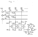
- FIG. 1 of the accompanying drawings schematically illustrates a so-called programmable device the contents of a ROM of which can be written in accordance with a user's needs - a field programmable device.
- a programmable ROM device has memory cells each of the junction breakdown type and each having the structure (in an unwritten state) of a transistor whose base is not wired.
- Such memory cells M " , M, 2 ... are connected at the points of intersection of word lines W, W 2 ... and bit lines B i , 8 2 ....
- a writing operation for writing data into a cell, is carried out in such a way that the cell is supplied with a writing current (programming current) to break down the emitter-base junction of the cell transistor (i.e. to bring the cell into its conductive state) and thus turn the cell into a P-N diode (e.g. M 12 or M 21 in Figure 1) formed of the base-collector junction of the transistor thereof.
- a writing current programming current
- the whole memory bit lines and word lines are sequentially selected in accordance with data to be written, and a writing operation is executed for each desired cell, each cell being located at the intersection point of a particular word line and a particular bit line.
- One problem with which the present inventors are concerned is the formation of a P-N-P-N structure between a cell in respect of which a writing operation has been completed and which cell has become a diode, and a cell in respect of which a cell writing operation has not been completed and which remains a transistor.
- writing current for writing into a cell needs to flow between a selected bit line and word line without turning such a P-N-P-N structure "on", to permit the writing current to be supplied to the cell to be written at the intersection point of the selected bit and word lines.
- the word lines of the ROM are formed of a diffused layer.
- the diffused layer has defects and in which a non-selected word line, which ought to hold a high withstand voltage during a writing operation, allows current to leak out
- programming (writing) current undesirably flows out to the substrate of a cell through a parasitic P-N-P transistor which is formed by the cell and the substrate.
- ⁇ a current gain factor
- a field programmable bipolar semiconductor memory device comprising a plurality of word lines, a plurality of bit lines arranged to cross the word lines, and a plurality of memory cells arranged in a single semiconductor substrate each connected to a bit line and a word line, characterised in that the device further comprises supply means operable for supplying non-selected word lines with a voltage sufficient to prevent turn-on of a parasitic P-N-P-N element formed by memory cells of the device, and operable for supplying non-selected word lines with a voltage sufficient to prevent leakage of a writing or programming current, delivered via a selected bit line, through a parasitic P-N-P transistor formed in a previously written or programmed memory cell on the selected bit line.
- non-selected word lines are word lines through which a writing or programming current delivered via bit line is not intended to flow when a memory cell is to be written or programmed.
- a selected bit line is a bit line through which the writing or programming current is to flow to a memory cell to be written or programmed.
- An embodiment of the present invention can provide a solution to the problems mentioned above and can provide a programmable device which is capable of stable and reliable programming.
- the turn-on of a P-N-P-N structure in a junction breakdown type memory (the P-N-P-N structure being formed by a memory cell into which data has been written and which has become a diode, and a memory cell into which data has not been written and which remains a transistor) can be prevented.
- a leakage current in a junction breakdown type memory which leakage current is attributable to a vertical type parasitic transistor which appears in the writing mode of the memory, is suppressed.
- WD indicates word drivers which drive corresponding word lines to H (high) or L (low) level.
- the circuit arrangement of a word driver consists of transistors Q 1 and Q 2 ( Figure 2) or Q 1 to Q 3 ( Figure 3), resistors R 1 to R 3 ( Figure 2) or R 1 and R 2 ( Figure 3) and a diode D.
- transistor Q 1 the input transistor, receives an output RD from a row decoder, and an output stage of the word driver (transistor Q 2 in Figure 2, transistors Q 2 and Q 3 in Figure 3) drives a word line W.
- the transistors Q 1 and Q 2 turn “on” (and in the case of Figure 3 the transistor Q 3 turns “off") so that the word line W becomes L level. This corresponds to a selected state of the word line W.
- the word driver of Figure 2 is of the so-called resistor drive type, whilst the word driver of Figure 3 is of the type provided with a so-called off-buffer.
- P 1 , P 2 ... are programming terminals which, in the writing mode of the programmable ROM, are supplied with writing current.
- writing current is fed from a constant-current source of 120 mA or so, and the corresponding voltage is approximately 15 V at maximum.
- Supply voltage V cc is 5 V.
- the word line W 1 is brought to L level by its corresponding word driver WD, and writing current is supplied from the terminal P 1 to the cell M 11 .
- This cell M 11 has its emitter-base junction broken down and becomes a diode which allows current to flow from the bit line B, to the word line W i .
- RR,, RR 2 , RR 3 are reading terminals which receive outputs from a column decoder when the P-ROM is in a reading mode.
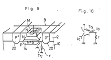
- Figure 4 illustrates the physical structure of essential portions of such a P-ROM.
- 10 is a P-type semiconductor substrate, which is formed with an N-type epitaxial layer 12 on its surface and an N + - type buried layer 14 within its interior.
- the epitaxial layer 12 is formed with P-type diffused regions 16, in each of which an N-type diffused region 18 is formed.
- Parts 12, 16 and 18 serve as the collector, base and emitter regions of a memory cell transistor, respectively. It is assumed that the memory cell M 11 , having such a structure, has not been written, whereas it is assumed that memory cell M 12 has been written, as in the illustration of Figure 1.
- the bit line B 2 Since the emitter-base junction of the written cell M 12 is in a shortcircuited state, the bit line B 2 has formed thereon a lateral P-N-P transistor (Tr, in the equivalent circuit diagram of Figure 5) which is constructed of the P-type region 16 of the cell M, 2 , the N-type layer 12, and the P-type region of the cell M 11 .
- the unwritten cell M 11 has a vertical transistor (Tr 2 in Figure 5) structure constituted by N-type layer 18 and P-type layer 16 thereof, and the N-type layer 12. These transistors Tr 1 and Tr 2 and the bit lines B 1 and B 2 are connected as shown in Figure 5.
- a P-N-P-N element in other words an element having a structure resembling that of a thyristor, is thus effectively connected between the bit lines B 2 and B i , that is, between the bit lines of the written cell and of the unwritten cell.
- this P-N-P-N element does not have a trigger terminal, it may seem that it would not turn "on".
- the N-type layer 12 which acts as the base of the lateral transistor Tr, and as the collector of the vertical transistor Tr 2 has a large capacitance C (see Figure 5) with respect to the ground of the P-ROM. Therefore, when a voltage is applied to the bit line 8 2 , a charging current flows through a path consisting of the bit line B 2 , the N-type layer 18 and the P-type layer 16, the N-type layer 12 and the capacitance C, and it triggers the P-N-P-N element.
- the transistor Tr is rendered conductive, with the aforementioned charging current acting as its base current, and a collector current flows therein.
- This collector current becomes the base current of the transistor Tr 2 , which renders the transistor Tr 2 conductive.
- the base current of the transistor Tr 1 is maintained by the transistor Tr 2 , so that the transistors Tr 1 and Tr 2 hold their "on” states even when the charging current disappears. That is, since the collector voltage of the transistor Tr 2 is fixed to a voltage about 0.2 V higher than that of the bit line B,, the base voltage of the transistor Tr, rises to prevent this transistor from turning "off”.
- the inventors of the present invention have arrived at a solution to this problem which in particular can cope with the problem in a junction breakdown type P-ROM.
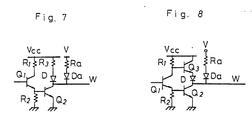
- FIGs 6A and 6B illustrate a first embodiment of the present invention.
- a high voltage V is applied from an external terminal T to word lines W i , W 2 ... through respective series circuits each of which consists of a resistor Ra and a diode Da.
- High voltage V may be supplied to the word lines through resistors Ra.
- charging of the capacitance C referred to above Figure 5 is effected on the basis of the voltage V applied to a word line, and there is no charging current based on the writing voltage applied to a bit line.
- the P-N-P-N element at Tr 1 and Tr 2 is not triggered by a flow of current through 8 2 , 18 and 16, 12 and C and does not turn "on", and data can be written into a memory cell, e.g. M 22 , by applying writing current thereto.
- FIG. 6B illustrates in more detail the first embodiment of the present invention as shown in Figure 6A. Like parts are designated by like references in Figures 1 and 6B.
- the sense amplifier SA functions to read out the contents of memory cells.
- Figures 7 and 8 illustrate second and third embodiments of the present invention in which high voltage V is applied to a word line W through a resistor Ra and a diode Da on the word driver sides of circuits as illustrated in Figures 2 and 3, respectively.
- Like parts are designated by like references in Figures 2, 3 and 7, 8. '
- a parasitic P-N-P transistor When leakage occurs between a word line and another region (e.g. the substrate of a P-ROM) as explained above, a parasitic P-N-P transistor, the presence of which is inherent in a P-N junction and whose collector is the substrate, turns "on", with the result that a current corresponding to its collector current i b . ⁇ (i b being the base current of the parasitic transistor) flows into the substrate. This phenomenon will be described with reference to Figures 9 and 10.
- the parasitic P-N-P transistor is a vertical transistor Tr 3 whose emitter is a P-type base region of a memory cell M, whose base is an N-type collector region (14) of the memory cell M and whose collector is a P-type substrate 10.
- Tr 3 When a leakage resistance r exists between the substrate 10 and the N-type layer 12 serving as a word line, the base current i b of the parasitic transistor Tr 3 flows in a written cell as illustrated in Figure 10, so that the transistor Tr 3 turns "on" to pass collector current i e , equal to i b . ⁇ , to the substrate.
- the P-ROM only a selected word line is at L level, with all other, non-selected, word lines at H level.
- a selected bit line is given a HH level (the high voltage level used during writing operations) in the programming mode. Accordingly, when a selected bit line has a written cell connected thereto even if the word line of this cell is not selected and is therefore at H level, the selected bit line is still at HH level, so that a current I b flows and the current of the selected bit line flows to the substrate through the written cell. In contrast, if HH voltage is applied to the word line W, or N-type layer 12, as it is in an embodiment of the present invention, the base current i b does not flow and the aforementioned current outflow to the substrate is avoided.
- 20 is a P + -type isolation region.
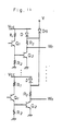
- Figure 11 shows a fourth embodiment of the present invention.
- the output stage of each word driver in Figure 11 (each word driver comprising resistors R 1 to R 3 , transistors Q 1 and Q 2 , and a diode D, and driving a respective word line W, ... W n ) consists of a transistor Q 2 and a resistor R 3 .
- the transistor Q 2 has its emitter grounded, and has its collector connected to one end of the resistor R 3 .
- the other ends of the resistors R 3 of the word drivers are connected to the cathodes of diodes D. Further, the cathode of a diode Da is connected to those of the diodes D.
- the anodes of the diodes D are connected to a voltage source V cc , and the anode of the diode Da is connected to a further voltage source V.
- the first to third embodiemnts of the present invention described above may require a number of pairs of resistors Ra and diodes Da equal to the number of the word lines, the embodiment of Figure 11 requires only one diode Da which is provided in common for all the word lines.
- respective diodes D are required for the word drivers, but the fourth embodiment of the present invention as shown can be modified and only one diode D employed in common for all the word drivers.
- the common diode D is connected to V cc and in common to resistors R 3 of the word drivers.
- the cathode of the diode D is connected to a common connection point of resistors R 3 and the anode of the diode D is connected to V cc .
- the cathode of diode Da is in this case connected to the common connection point of resisors R 3 and its anode is connected to voltage source V.
- the voltage V to be applied to a word line is a fixed voltage which is preferably at least 0.8 V higher than the writing voltage to be applied to a bit line.
- This fixed voltage is applied to all the word lines in common.
- current flows through a path consisting of the resistor Ra, the diode Da and the output transistor Q 2 in the second and third embodiments of the present invention, and flows through a path consisting of diode Da, resistor R 3 and output transistor Q 2 in the case of the fourth embodiment of the present invention.
- This current is limited by the resistor Ra or by the resistor R 3 .
- the constant-current source needs to include provision for a component which corresponds to the aforementioned current flowing through the path provided by Ra, Da and Q 2 or the path provided by R 3 , Da and Q 2 .
- Embodiments of the present invention are effective when applied to programmable devices employing memory cells of any of the above-mentioned kinds.
- Schottky diodes may be used as the above-mentioned diodes Da and D.
- the turn-on of a parasitic P-N-P-N element and the outflow of writing current to substrate attributable to the presence of a parasitic P-N-P transistor can be hindered in the programming mode of a programmable device by the simple expedient of applying high voltage to word lines.
Landscapes
- Read Only Memory (AREA)
- Semiconductor Memories (AREA)
Applications Claiming Priority (2)
| Application Number | Priority Date | Filing Date | Title |
|---|---|---|---|
| JP2972781A JPS57143798A (en) | 1981-03-02 | 1981-03-02 | Programmable element |
| JP29727/81 | 1981-03-02 |
Publications (3)
| Publication Number | Publication Date |
|---|---|
| EP0059630A2 EP0059630A2 (en) | 1982-09-08 |
| EP0059630A3 EP0059630A3 (en) | 1983-10-19 |
| EP0059630B1 true EP0059630B1 (en) | 1986-10-22 |
Family
ID=12284128
Family Applications (1)
| Application Number | Title | Priority Date | Filing Date |
|---|---|---|---|
| EP82301020A Expired EP0059630B1 (en) | 1981-03-02 | 1982-03-01 | Field programmable device |
Country Status (5)
| Country | Link |
|---|---|
| US (1) | US4488261A (enExample) |
| EP (1) | EP0059630B1 (enExample) |
| JP (1) | JPS57143798A (enExample) |
| DE (1) | DE3273919D1 (enExample) |
| IE (1) | IE53338B1 (enExample) |
Families Citing this family (9)
| Publication number | Priority date | Publication date | Assignee | Title |
|---|---|---|---|---|
| JPS592291A (ja) * | 1982-06-28 | 1984-01-07 | Fujitsu Ltd | プログラマブル・リ−ドオンリ・メモリ装置 |
| JPS5922295A (ja) * | 1982-06-30 | 1984-02-04 | Fujitsu Ltd | 半導体記憶装置 |
| DE3409776A1 (de) * | 1983-03-17 | 1984-09-20 | ROMOX Inc., Campbell, Calif. | In einer kassette angeordneter, wiederprogrammierbarer speicher sowie verfahren zu dessen programmierung |
| JPS6095799A (ja) * | 1983-10-31 | 1985-05-29 | Nec Corp | プログラマブル・リ−ド・オンリ−・メモリ |
| JPS61150199A (ja) * | 1984-12-25 | 1986-07-08 | Nec Corp | 半導体記憶装置 |
| FR2623016B1 (fr) * | 1987-11-06 | 1991-06-14 | Thomson Semiconducteurs | Dispositif de fusion d'un fusible dans un circuit integre de type cmos |
| US5892683A (en) * | 1993-03-31 | 1999-04-06 | Altera Coporation | Program compatibility recognition for a programmable logic device |
| WO2004090909A1 (ja) * | 1994-12-27 | 2004-10-21 | Nobufumi Inada | 情報記憶装置およびその動作方法 |
| US7376008B2 (en) * | 2003-08-07 | 2008-05-20 | Contour Seminconductor, Inc. | SCR matrix storage device |
Family Cites Families (6)
| Publication number | Priority date | Publication date | Assignee | Title |
|---|---|---|---|---|
| US3742592A (en) * | 1970-07-13 | 1973-07-03 | Intersil Inc | Electrically alterable integrated circuit read only memory unit and process of manufacturing |
| US3733690A (en) * | 1970-07-13 | 1973-05-22 | Intersil Inc | Double junction read only memory and process of manufacture |
| JPS55142475A (en) * | 1979-04-23 | 1980-11-07 | Fujitsu Ltd | Decoder circuit |
| JPS5828680B2 (ja) * | 1979-04-27 | 1983-06-17 | 富士通株式会社 | 半導体記憶装置 |
| US4237547A (en) * | 1979-09-17 | 1980-12-02 | Motorola, Inc. | Program decoder for shared contact eprom |
| US4312047A (en) * | 1980-05-29 | 1982-01-19 | Motorola, Inc. | Memory array having improved isolation between sense lines |
-
1981
- 1981-03-02 JP JP2972781A patent/JPS57143798A/ja active Granted
-
1982
- 1982-03-01 US US06/353,356 patent/US4488261A/en not_active Expired - Fee Related
- 1982-03-01 IE IE454/82A patent/IE53338B1/en not_active IP Right Cessation
- 1982-03-01 EP EP82301020A patent/EP0059630B1/en not_active Expired
- 1982-03-01 DE DE8282301020T patent/DE3273919D1/de not_active Expired
Also Published As
| Publication number | Publication date |
|---|---|
| US4488261A (en) | 1984-12-11 |
| IE53338B1 (en) | 1988-10-26 |
| EP0059630A2 (en) | 1982-09-08 |
| EP0059630A3 (en) | 1983-10-19 |
| JPS57143798A (en) | 1982-09-06 |
| IE820454L (en) | 1982-09-02 |
| JPS616476B2 (enExample) | 1986-02-26 |
| DE3273919D1 (en) | 1986-11-27 |
Similar Documents
| Publication | Publication Date | Title |
|---|---|---|
| US4396999A (en) | Tunneling transistor memory cell | |
| US4347586A (en) | Semiconductor memory device | |
| JPS619895A (ja) | 半導体記憶回路 | |
| EP0059630B1 (en) | Field programmable device | |
| US3872450A (en) | Fusible link memory cell for a programmable read only memory | |
| EP0140368B1 (en) | Programmable read-only memory device provided with test cells | |
| US3849675A (en) | Low power flip-flop circuits | |
| US4432070A (en) | High speed PROM device | |
| US4604728A (en) | Semiconductor memory device | |
| EP0019381B1 (en) | Semiconductor memory device with address signal level setting | |
| US4599688A (en) | Semiconductor memory device having switching circuit for preventing channel leakage in constant current source | |
| EP0018192B1 (en) | Bipolar programmable read only memory device including address circuits | |
| EP0028157B1 (en) | Semiconductor integrated circuit memory device with integrated injection logic | |
| US3603820A (en) | Bistable device storage cell | |
| EP0381120A2 (en) | High speed ECL input buffer for vertical fuse arrays | |
| US4488263A (en) | Bypass circuit for word line cell discharge current | |
| US3979735A (en) | Information storage circuit | |
| EP0006702B1 (en) | Semiconductor integrated memory circuit | |
| EP0306663B1 (en) | Fast write saturated memory cell | |
| EP0252780B1 (en) | Variable clamped memory cell | |
| IE52801B1 (en) | Semiconductor memory circuit device | |
| US4899311A (en) | Clamping sense amplifier for bipolar ram | |
| JPS581919Y2 (ja) | メモリ回路 | |
| EP0080351A2 (en) | Multi-emitter transistors in semiconductor memory devices | |
| US5383153A (en) | Semiconductor memory device with flash-clear function |
Legal Events
| Date | Code | Title | Description |
|---|---|---|---|
| PUAI | Public reference made under article 153(3) epc to a published international application that has entered the european phase |
Free format text: ORIGINAL CODE: 0009012 |
|
| AK | Designated contracting states |
Designated state(s): DE FR GB NL |
|
| PUAL | Search report despatched |
Free format text: ORIGINAL CODE: 0009013 |
|
| AK | Designated contracting states |
Designated state(s): DE FR GB NL |
|
| 17P | Request for examination filed |
Effective date: 19840406 |
|
| GRAA | (expected) grant |
Free format text: ORIGINAL CODE: 0009210 |
|
| AK | Designated contracting states |
Kind code of ref document: B1 Designated state(s): DE FR GB |
|
| ET | Fr: translation filed | ||
| REF | Corresponds to: |
Ref document number: 3273919 Country of ref document: DE Date of ref document: 19861127 |
|
| PLBE | No opposition filed within time limit |
Free format text: ORIGINAL CODE: 0009261 |
|
| STAA | Information on the status of an ep patent application or granted ep patent |
Free format text: STATUS: NO OPPOSITION FILED WITHIN TIME LIMIT |
|
| 26N | No opposition filed | ||
| PGFP | Annual fee paid to national office [announced via postgrant information from national office to epo] |
Ref country code: GB Payment date: 19940221 Year of fee payment: 13 |
|
| PGFP | Annual fee paid to national office [announced via postgrant information from national office to epo] |
Ref country code: DE Payment date: 19940224 Year of fee payment: 13 |
|
| PGFP | Annual fee paid to national office [announced via postgrant information from national office to epo] |
Ref country code: FR Payment date: 19940310 Year of fee payment: 13 |
|
| PG25 | Lapsed in a contracting state [announced via postgrant information from national office to epo] |
Ref country code: GB Effective date: 19950301 |
|
| GBPC | Gb: european patent ceased through non-payment of renewal fee |
Effective date: 19950301 |
|
| PG25 | Lapsed in a contracting state [announced via postgrant information from national office to epo] |
Ref country code: FR Free format text: LAPSE BECAUSE OF NON-PAYMENT OF DUE FEES Effective date: 19951130 |
|
| PG25 | Lapsed in a contracting state [announced via postgrant information from national office to epo] |
Ref country code: DE Effective date: 19951201 |
|
| REG | Reference to a national code |
Ref country code: FR Ref legal event code: ST |