EP0080351A2 - Multi-emitter transistors in semiconductor memory devices - Google Patents
Multi-emitter transistors in semiconductor memory devices Download PDFInfo
- Publication number
- EP0080351A2 EP0080351A2 EP82306186A EP82306186A EP0080351A2 EP 0080351 A2 EP0080351 A2 EP 0080351A2 EP 82306186 A EP82306186 A EP 82306186A EP 82306186 A EP82306186 A EP 82306186A EP 0080351 A2 EP0080351 A2 EP 0080351A2
- Authority
- EP
- European Patent Office
- Prior art keywords
- transistor
- type region
- read
- pnpn
- current
- Prior art date
- Legal status (The legal status is an assumption and is not a legal conclusion. Google has not performed a legal analysis and makes no representation as to the accuracy of the status listed.)
- Granted
Links
- 239000004065 semiconductor Substances 0.000 title claims abstract description 18
- 230000015654 memory Effects 0.000 claims abstract description 67
- 238000003199 nucleic acid amplification method Methods 0.000 claims abstract description 20
- 230000003321 amplification Effects 0.000 claims abstract description 19
- 230000003247 decreasing effect Effects 0.000 claims description 12
- 239000012535 impurity Substances 0.000 claims description 6
- 238000007599 discharging Methods 0.000 description 13
- 238000010586 diagram Methods 0.000 description 8
- 230000002411 adverse Effects 0.000 description 7
- 239000008186 active pharmaceutical agent Substances 0.000 description 5
- 238000001514 detection method Methods 0.000 description 5
- 230000003071 parasitic effect Effects 0.000 description 5
- 230000003068 static effect Effects 0.000 description 4
- 239000000758 substrate Substances 0.000 description 3
- 238000002955 isolation Methods 0.000 description 2
- 230000000630 rising effect Effects 0.000 description 2
- 238000007796 conventional method Methods 0.000 description 1
- 230000003111 delayed effect Effects 0.000 description 1
- 230000006866 deterioration Effects 0.000 description 1
- 238000009792 diffusion process Methods 0.000 description 1
- 238000005468 ion implantation Methods 0.000 description 1
- 238000004519 manufacturing process Methods 0.000 description 1
- 238000000034 method Methods 0.000 description 1
- 238000005215 recombination Methods 0.000 description 1
- 230000006798 recombination Effects 0.000 description 1
- 229920006395 saturated elastomer Polymers 0.000 description 1
Images


Classifications
-
- H—ELECTRICITY
- H01—ELECTRIC ELEMENTS
- H01L—SEMICONDUCTOR DEVICES NOT COVERED BY CLASS H10
- H01L27/00—Devices consisting of a plurality of semiconductor or other solid-state components formed in or on a common substrate
- H01L27/02—Devices consisting of a plurality of semiconductor or other solid-state components formed in or on a common substrate including semiconductor components specially adapted for rectifying, oscillating, amplifying or switching and having potential barriers; including integrated passive circuit elements having potential barriers
- H01L27/0203—Particular design considerations for integrated circuits
- H01L27/0214—Particular design considerations for integrated circuits for internal polarisation, e.g. I2L
- H01L27/0229—Particular design considerations for integrated circuits for internal polarisation, e.g. I2L of bipolar structures
- H01L27/0233—Integrated injection logic structures [I2L]
- H01L27/0237—Integrated injection logic structures [I2L] using vertical injector structures
-
- G—PHYSICS
- G11—INFORMATION STORAGE
- G11C—STATIC STORES
- G11C11/00—Digital stores characterised by the use of particular electric or magnetic storage elements; Storage elements therefor
- G11C11/21—Digital stores characterised by the use of particular electric or magnetic storage elements; Storage elements therefor using electric elements
- G11C11/34—Digital stores characterised by the use of particular electric or magnetic storage elements; Storage elements therefor using electric elements using semiconductor devices
- G11C11/40—Digital stores characterised by the use of particular electric or magnetic storage elements; Storage elements therefor using electric elements using semiconductor devices using transistors
- G11C11/41—Digital stores characterised by the use of particular electric or magnetic storage elements; Storage elements therefor using electric elements using semiconductor devices using transistors forming static cells with positive feedback, i.e. cells not needing refreshing or charge regeneration, e.g. bistable multivibrator or Schmitt trigger
- G11C11/411—Digital stores characterised by the use of particular electric or magnetic storage elements; Storage elements therefor using electric elements using semiconductor devices using transistors forming static cells with positive feedback, i.e. cells not needing refreshing or charge regeneration, e.g. bistable multivibrator or Schmitt trigger using bipolar transistors only
- G11C11/4116—Digital stores characterised by the use of particular electric or magnetic storage elements; Storage elements therefor using electric elements using semiconductor devices using transistors forming static cells with positive feedback, i.e. cells not needing refreshing or charge regeneration, e.g. bistable multivibrator or Schmitt trigger using bipolar transistors only with at least one cell access via separately connected emittors of said transistors or via multiple emittors, e.g. T2L, ECL
Definitions
- the present invention relates to multi-emitter transistors in semiconductor memory devices, for example a random access memory (RAM) having bipolar static memory cells with PNPN transistor cells.
- RAM random access memory
- a typical semiconductor memory comprises a plurality of word lines, a plurality of bit lines, and a plurality of memory cells located at the cross points of the word lines and bit lines.
- Semiconductor memories utilize various types of memory cells.
- the present invention can be applied to a semiconductor memory utilizing saturation-type memory cells.
- a so-called holding current flows through each memory cell so as to maintain the stored data of logic "1" or "0".
- the holding current When the memory cell is to be changed from a half selected state to a nonselected state, electric charges stored in the parasitic capacitances of the cell are discharged by the holding current.
- the greater the holding current the faster the switching speed from the half selected state to the norselected state.
- the discharged holding current IS
- the discharged holding current should preferably be small.
- I DS discharging current
- the emitter voltage of a detection transistor i.e., a read/write transistor
- the detection transistor operates inversely, as hereinafter described in detail, so that a part of the discharging current (I DS ) from the word line is unnecessarily branched as a sink current into the bit line connected to the detection transistor of each halfselected memory cell. This sink current adversely affects the rising speed of the word line potential.
- a bit-line clamping circuit for clamping nonselected bit lines to a level higher than the level of the selected word line.
- the sink current also flows through each half selected memory cell in the selected word line.
- An embodiment of the present invention can be made to provide a semiconductor memory device in which the current amplification factor ⁇ u of each detecting transistor when it is operated inversely is controlled so that the factor y is made small, whereby the switching speed of each word line when it is switched from a selected state to a nonselected state is increased without increasing the discharging current.
- Figure 1 is an equivalent circuit diagram of a well known bipolar memory cell constructed by PNPN transistors.
- a PNP transistor Q 1 and an NPN transistor Q 3 comprises a first PNPN transistor
- a PNP transistor Q 2 and an NPN transistor Q 4 comprise a second PNPN transistor.
- the first PNPN transistor and the second PNPN transistor are crosss-coupled with each other.
- a pair of bit lines B and B 1 are connected to the emitters of transistors Q 5 and Q 6 , respectively.
- a word line W + is connected to the emitters of the PNP transistors Q 1 and Q 2 .
- Another word line W is connected to the emitters of the NPN transistors Q 3 and Q 4 .
- a write data is supplied to the bit line B 0 or B 1 so that either the first or the second PNPN transistor is turned on.
- a current must be passed through the transistor Q 5 .
- a current must be passed through the transistor Q 6 .
- Either the data "1" or "0" is stored in the memory cell, depending or whether the first PNPN transistor or the second PNPN transistor is conductive. The stored data can be detected'or read out through the transistor Q 5 or Q 6 to the bit line B 0 or B 1 . Therefore, the transistors Q 5 and Q 6 are hereinafter referred to as read/write (R/W) transistors, and the transistors Q 3 and Q 4 are hereinafter referred to as holding transistors.
- Figure 2 is a cross-sectional view of the physical structure of the first PNPN transistor shown in Fig. 1.
- Fig. 2 on a P-type substrate 1, an N + -type buried layer 2 is formed. Isolation regions 3 and 4 are formed on both sides of the element region of the first PNPN transistor.
- N + -type buried layer 2 On the N + -type buried layer 2, an N-type region 5 for collectors of the transistors Q 3 and Q 5 is formed.
- a P-type region 6 for the emitter of the PNP transistor Q 1 is formed.
- a P-type region 7 for the bases of the transistors Q 3 and Q 5 and also for the collector of the transistor Q 1 is formed.
- an N -type region 8 for the emitter of the transistor Q 3 and an N + -type region 9 for the emitter of the transistor Q 5 are formed.
- the electrode on the region 5 is connected to the collectors C 3 and C 5 of the transistors Q 3 and Q 5 .
- the electrode on the region 6 is connected to the word line W .
- the electrode on the region 7 is connected to the based B 3 and B 5 of the transistors Q 3 and Q 5 .
- the electorde on the region 8 is connected to the emitter E 3 of the transistor Q 3 .
- the electrode on the region 9 is connected to the emitter E 5 of the transistor Q 5 .
- the regions 5, 6, and 7 constitute the lateral PNP transistor Q 1 .
- the regions 8, 7, 5, and 2 constitute the vertical NPN transistor Q 3 .
- the R/W transistor Q 5 is formed by the regions 9, 7, 5, and 2.
- the transistors Q 3 and Q 5 have a common base, common collector, but different emitters. Therefore, the transistors Q 3 and Q 5 are formed as a multiemitter transistor.
- the second PNPN transistor has a physical structure similar to the structure of the first PNPN transistor.
- a PNPN memory cell can hold data when it satisfies the conduction condition: ⁇ PNP + ⁇ NPN > 1 where ⁇ PNP is the current amplification factor of the PNP transistor Q 1 or Q 2 when its base is grounded, and a NPN is the current amplification factor of the NPN transistor Q 3 or Q 4 when its base is grounded.
- ⁇ PNP is greater than 0.8 and ⁇ NPN is nearly equal to 1. Therefore, the above conduction condition can be satisfied even when the holding current is considerably small.
- a PNPN memory cell can hold data by using a holding current which is smaller by one or two orders than that of a conventional static memory cell. Accordingly, a PNPN memory cell is suitable for a low-power RAM and for a large-capacity RAM.
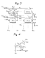
- FIG. 3 is a circuit diagram of a main portion of a memory-cell array constructed by the PNPN memory cells of Fig. 1.
- transistors Q X1 , Q X2 , ... are those for driving word lines W 1+ , W 2+ , ..., respectively.
- a high voltage V XH is applied to the base of the transistor Q X1 or Q X2 .
- V XL is applied to the base of the transistors Q X1 or Q X2
- the word line W 1+ or W 2+ is in an nonselected state.
- Holding current sources SI H1 , SI H2 , ... are connected to the word lines W 1- W 2- , ... , respectively for conducting holding currents I H1 , I H2 , ... through the word lines W 1- , W 2 -, ...
- the first problem is as follows.
- the word line W 1+ changes from the selected state to the nonselected state, electric charges, stored in parasitic capacitances in each of the memory cells Cell , ..., C eln connected to the word line W 1+ , are discharged.
- the parasitic capacitances are mainly the capacitances C o or C 1 between the collector of the transistors Q 3 and Q and the substrate or between the collector of the transistors Q 4 and Q 6 and the substrate.
- each of the holding currents I H1 , I H2 , ... in Fig. 3 is smaller than that of a conventional static memory cell by one or two orders.
- the current for discharging the electric charges stored in the parasitic capacitances is so small that it takes a considerably long time to discharge the electric charges and, accordingly, to change a word line from the selected state to the nonselected state.
- a double selected state may be produced. That is, within a certain time period, a word line which is changing from a selected state to a nonselected state and another word line which is changing from a nonselected state to a selected state may have the same electric potential as each other.
- the read time is delayed in a reading cycle, and a write error operation may be caused in a writing cycle.
- a discharging circuit connected to each word line W 1- , W 2- , ... has previously been proposed (see, for example, Japanese Patent Application No. 54-110720 or Japanese Unexamined Patent Publication (Kokai) No. 56-37884).
- the discharging circuit can selectively absorb a discharging current I DS from a word line which is changing from a selected state to a nonselected state.
- the electric charges along the selected word lines W + , W - are discharged together with not only the holding current I H but also the discharging current I DS , that is, in a form of I H + I DS .
- the discharging circuit for each word line is especially indispensable.
- the second problem in the circuit of Fig. 3 will be described with reference to Fig. 4.
- the second problem is one caused by an inverse operation of the R/W transistor Q5 or Q 6 .
- Fig. 4 only the first PNPN memory cell is illustrated.
- the first PNPN memory cell of Fig. 4 is in a conductive state, both the PNP transistor Q 1 and the NPN transistor Q 3 are saturated, so that their base-collector junctions are forwardly biased. That is, the base potential of the multiemitter transistor Q 3 or Q 5 is slightly higher than its collector potential.
- the R/W transistor Q 5 is caused to be operated in an inverse mode. That is, the emitter of the transistor Q 5 acts as a collector and, thereby, a sink current i SNK flows from the bit line B 0 through the emitter of the R/W transistor Q 5 and the emitter of the transistor Q 3 to the word line W_.
- the source of this sink current i SNK is the holding current source SI H .
- This sink current i SNK causes the following adverse influences in the memory cell array. Referring back to Fig. 3, the selected word line, for example the word line W 1+ , has a higher potential than the nonselected word lines. Therefore, the potential of each bit line is determined by the memory cell connected between this bit line and the selected word line.
- the emitters of the R/W transistors Q 5 or Q 6 in all of the nonselected word lines are inversely biased.
- the sink current i SNK flows from either one of the pair of bit lines B 0 and B 1 through the emitter of the R/W transistor Q 5 or Q 6 to the emitter of the transistor Q 3 or Q 4 in the conducting PNPN transistor.
- the first PNPN transistor at the side of the bit line B 10 is conductive, so that the sink current i SNK flows from the bit line B 10 into the memory cell C e21 .
- the second PNPN transistor at the side of the bit line B n1 is conductive, so that the sink current i SNK flows from the bit lines B n1 into the memory cell C e2n .
- All of the sink currents i SNK flowing into all of the memory cells in all of the nonselected word columns are supplied from the selected word line, for example, the word line W 1+ , through the half selected memory cells.
- the total sink currents I SNK supplied from the selected word line can thus be expressed as: where N is the number of memory cells in the nonselected word columns.
- the total sink current I SNK causes the potential of the selected word line to be lowered.
- the transistor for example Q X1
- the transistor for example Q X1
- the transistor for example Q X1
- the potential difference between the base and the emitter of the transistor Q X1 is increased, so that the base potenital of the transistor Q X1 is lowered.
- the current to be supplied to a nonselected word line is decreased by the sink current i SNK as illustrated in Fig. 4. Therefore, the potential of the nonselected word line is increased due to the sink current iSNK.
- the margin between the potentials of a selected word line and of a nonselected word line is narrowed due to the sink current i SNK flowing into each nonselected memory cell.
- the driving ability of the transistor Q X1 or Q X2 for driving a word line to be selected is lowered, causing a lowered switching speed and an increase in reading time of the RAM.
- a countermeasure for the adverse influences of the sink current i SNK has already been proposed.
- a clamp circuit is provided to correspond to each pair of bit lines.
- the clamp circuit clamps the potentials of all of nonselected bit lines to a level higher than the level determined by the selected word line, so that the sink current i SNK is supplied from the clamp circuit.
- the selected pair of bit lines is, of course, not clamped so as to allow the detection of a potential difference between them.
- Figure 5 is a circuit diagram illustrating a conventional memory cell array in which the countermeasures for the above-mentioned first and second problems, i.e., the problem of the word-line discharging and the problem of the sink currents i SNK , are provided.
- diodes D 1 and D 2 connected to the word line W 1- and W 2- respectively are for supplying a discharge current I DS to a selected word line.
- the cathodes of these diodes D 1 , D 2 , ... are commonly commected to a discharge current source SI D .
- Transistors Q B11 , Q B12 , ... , Q Bn1 , and Q Bn2 are for clamping nonselected bit lines to a level for a reference potential V CL higher than the potential of the selected word line.
- Q Yn1 , and Q Yn3 are for selecting the bit lines B 10 ' B 11 , . ⁇ , B no , and B n1 , respectively.
- Transistors Q Y12 , ... , and Q Yn2 are for invalidating the clamping transistors Q B11 , Q B12 , ... , Q Bn1 , and Q Bn2 when corresponding bit lines are,selected.
- bit lines B 10 and B 11 are selected so that bit currents I B0 and I B1 are supplied from current sources SI B0 and SI B1 to the bit lines B 10 and B 11 , respectively.
- the transistor Q Y12 is turned on so that the base potential of the clamping transistors Q B11 and Q B12 is lowered by a voltage drop across the resistor R 1 .
- the clamping transistors Q B11 and Q B12 are turned off.
- the transistors Q Yi1 , Q yi2 , and Q Yi3 are kept in their off state. Therefore, the clamping transistors Q Bi1 and Q Bi2 are kept in their on state, so that the nonselected bit lines B i0 and B i1 are clamped to a high potential higher than the reference voltage V CL , which is higher than the potential of the selected word line.
- the potentials of the selected bit lines B 10 and B 11 are, of course, determined by the selected memory cell.
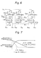
- the conventional device of Fig. 5 still involves the following problem, as explained with reference to Fig. 6.
- Figure 6 illustrates a part of the memory cell array of F ig. 5, in which the memory cells C el2 , C el3 , ... , and C eln in the selected word column are shown, but the selected memory cell C e11 is not shown.
- all of the nonselected bit lines are clamped to a level higher than the reference voltage V CL . Therefore, the R/W transistor in each of the half selected memory cells C el2 , C el3 , ... , and C eln also operates inversely as the R/W transistors in the nonselected word columns do.
- a sink current i SNK flows from V CL through, for example, the clamping transistor Q 21 and the conducting side in the memory cell C el2 to the word line W 1 -.
- the sink currents also flow through their conducting sides.
- the word-line discharging current I DS is selectively supplied to the word line W 1- .
- the holding current flowing through one memory cell is i H and that the word-line discharging current flowing through one memory cell is i DS .
- the sink current i SNK is expressed as: Where Y is a constant smaller than 1, representing the ratio between i SNK and (i H + iDS).
- Y is a constant smaller than 1, representing the ratio between i SNK and (i H + iDS).
- the discharge current i DS flowing through the word line W includes an invalid component. That is, the efficiency of the discharge current I DS supplied to the word line W 1- can be expressed as (1- ⁇ ).
- the constant Y is made small so that the efficiency of the discharge current is increased and the switching speed of the word line from the selected state to the nonselected state is increased without incerasing the discharge current.
- the constant Y determines the ratio of the sink current i SNK with respect to the supplied current (i H + i DS ) to one memory cell. Since the sink current i SNK flows as a result of the inverse operation mode of the R/W transistor, it will easily be seen that the constant y is proportional to the current amplification factor ⁇ u of the R/W transistor when it is inversely operated. Therefore, the constant Y can be made small by decreasing the current amplification factor ⁇ u.
- Figure 7 is a graph for explaining the switching operation of the word line. As will be apparent from Fig. 7, the smaller the constant Y , the faster the switching speed of the word line from the selected state to the nonselected state.
- Figure 8 is a cross-sectional view illustrating the physical structure of a half memory cell.
- the same portions are denoted by the same reference numerals or characters.
- the differences in Figs. 2 and 8 are that, instead of the R/W transistor Q 5 in Fig. 2, an R/W transistor Q 5a is provided in Fig. 8.
- the R/W transistor Q 5a has, instead of the P-type region 7 for the base of the R/W transistor Q 5 in Fig. 2, a P -type region 7a for the base of the R/W transistor Q 5a .
- the concentration of P-type impurity is made higher than the other P-type region 7 or 6.
- This high concentration of the P + -type region 7a can easily be formed by, for example, the ion-implantation technique.
- the current amplification factor ⁇ u of the R/W transistor when it is inversely operated is determined by the amount of the electrons which can reach the N + -type region 9 for the emitter E 5 from the P + -type region 7a. Since the concentration of the P-type impurity in the P +- type region 7a is increased, the amount of electrons injected into the P * -type region 7a is decreased and also the amount of electrons recombined with the P-type impurities within this P + -type region 7a is increased. Therefore, the amount of electrons which can reach the N + -type region 9 for the emitter E 5 is decreased. Thus, the current amplification factor ⁇ u of the R/W transistor Q 5a when it is inversely operated is decreased.
- Figure 9 illustrates another embodiment of the present invention.
- the difference between Fig. 8 and Fig. 9 are that, instead of forming the NPN transistor Q 3 between the PNP transis Q 1 and the R/W transistor Q 5a in Fig. 8, an R/W transistor Q 5b is formed between a PNP transistor Q lb and an NPN transistor Q 3b .
- the transistors Q 5b and Q 3b have . the common P-type region 7 for their bases B 3 and B 5 . It should be noted from Fig.
- a P-type region 7b the thickness of the P-type region 7 under the N +- type region 9 for the emitter E 5 of the R/W transistor Q 5b , which is referred to as a P-type region 7b, is greater than the thickness of the P-type region 7 under the N +- type region 8 for the emitter E 3 of the PNP transistor Q 3b .
- a P-type region 6b is provided for the emitter of the PNP transistor Q 1b .
- the P-type region 6b is made as thick as the P-type region 7b.
- the P-type region 7b for the base of the R/W transistor Q 5b thicker than the P-type region 7 for the base of the NPN transistor Q 3b , it takes a long time for the electrons, injected into the P-type region 7b for the base. of the transistor Q 5b , to reach the N -type region 9 for the emitter E 5 . Therefore, in the P-type region 7b, the probability of recombination of the injected electrons with the P-type imparities is increased. Thus, the current amplification factor 3u of the R/W transistor Q 5b when it is inversely operated can be made small.
- the P-type region 6b for the emitter, of the lateral PNP transistor Q lb is made as thick as the P-type region 7b by the same diffusion process, the areas of the P-type region 6b and the P-type region 7b opposite to each other are increased, so that the current amplification factor of the PNP transistor Q lb can be improved.
- the structures are employed for the purpose of decreasing the current amplification factor of only the R/W transistor when it is inversely operated. It might be thought that no problem will occur in operation when the structure for decreasing the inverse-current amplification factor is employed not only for the R/W transistor but also for the holding transistor Q 3 in Fig. 8 or the holding transistor Q 3b in Fig. 9, as long as the aforementioned holding condition: is satisfied.
- the structure for decreasing the inverse-current-amplification factor is adapted to the base portion of the holding transistor Q 3 in Fi g. 8 or Q 3b in Fig. 9, its forward current amplification factor ⁇ NPN is also decreased. Therefore, the margin for the holding condition is narrowed.
- the switching speed of a word line from a selected state to a nonselected state can be increased so that the read-out time of a RAM is shortened and the margin for preventing write-error operation is expanded.
Landscapes
- Engineering & Computer Science (AREA)
- Microelectronics & Electronic Packaging (AREA)
- Power Engineering (AREA)
- Computer Hardware Design (AREA)
- Physics & Mathematics (AREA)
- Condensed Matter Physics & Semiconductors (AREA)
- General Physics & Mathematics (AREA)
- Semiconductor Memories (AREA)
- Static Random-Access Memory (AREA)
- Bipolar Transistors (AREA)
Abstract
Description
- The present invention relates to multi-emitter transistors in semiconductor memory devices, for example a random access memory (RAM) having bipolar static memory cells with PNPN transistor cells.
- A typical semiconductor memory comprises a plurality of word lines, a plurality of bit lines, and a plurality of memory cells located at the cross points of the word lines and bit lines. Semiconductor memories utilize various types of memory cells. The present invention can be applied to a semiconductor memory utilizing saturation-type memory cells.
- Generally, in such a semiconductor memory, that is, a static semiconductor memory, a so-called holding current flows through each memory cell so as to maintain the stored data of logic "1" or "0". When the memory cell is to be changed from a half selected state to a nonselected state, electric charges stored in the parasitic capacitances of the cell are discharged by the holding current. The greater the holding current, the faster the switching speed from the half selected state to the norselected state. However, from the viewpoint of large memory capacity and low power consumption, the discharged holding current (IS) should preferably be small. Thus, it is difficult to increase the switching speed by making the holding current large. One previous proposal to get around this problem and achieve a fast switching speed is to have a discharging current (IDS) selectively absorbed from a selected word line.
- In such a semiconductor memory, the emitter voltage of a detection transistor, i.e., a read/write transistor, in each half selected memory cell is usually raised to a high level to prevent adverse influences of a sink current as hereinafter described in detail. However, when the emitter voltage is raised to a high level, the detection transistor operates inversely, as hereinafter described in detail, so that a part of the discharging current (IDS) from the word line is unnecessarily branched as a sink current into the bit line connected to the detection transistor of each halfselected memory cell. This sink current adversely affects the rising speed of the word line potential. Conventionally, in order to prevent the deterioration of the rising speed of the word line, a bit-line clamping circuit for clamping nonselected bit lines to a level higher than the level of the selected word line is provided. However, in this case, the sink current also flows through each half selected memory cell in the selected word line. The sink current iSNK for each memory cell is expressed as: iSNK = γ(iH+ iDS), where y is a factor proportional to the current amplification factor βu of the detection transistor when it is operated inversely, and iH and iDS are a holding current and a discharging current for each memory cell, respectively. It is preferable that the sink current iSNK be as small as possible so as to ensure a fast switching operation.
- An embodiment of the present invention can be made to provide a semiconductor memory device in which the current amplification factor βu of each detecting transistor when it is operated inversely is controlled so that the factor y is made small, whereby the switching speed of each word line when it is switched from a selected state to a nonselected state is increased without increasing the discharging current.
- Reference will now be made, by way of example, to the accompanying drawings, wherein:
- Fig. 1 is an equivalent circuit diagram of a known bipolar memory cell constructed by PNPN transistors;
- Fig. 2 is a cross-sectional view illustrating the physical structure of a conventional PNPN transistor shown in Fig. 1;
- Fig. 3 is a circuit diagram illustrating a main portion of a memory cell array constructed of the PNPN memory cells of Fig. 1;
- Fig. 4 is a circuit diagram of a half of the PNPN memory cell of Fig. 1;
- Fig. 5 is a circuit diagram illustrating another conventional memory cell array;
- Fig. 6 is a circuit diagram illustrating a part of the memory cell array in a selected word column other than the selected memory cell;
- Fig.' 7 is a graph;
- Fig. 8 is a cross-sectional view illustrating a physical structure of a half cell of a semiconductor memory device according to an embodiment of the present invention; and
- Fig. 9 is a crosssectional view illustrating the physical structure of a half cell of a semiconductor memory device according to another embodiment of the present invention.
- Before describing the embodiments of the present invention, conventional techniques and their problems will first be described with reference to Figs. 1 through 6.
- Figure 1 is an equivalent circuit diagram of a well known bipolar memory cell constructed by PNPN transistors. In Fig. 1, a PNP transistor Q1 and an NPN transistor Q3 comprises a first PNPN transistor, and a PNP transistor Q2 and an NPN transistor Q4 comprise a second PNPN transistor. The first PNPN transistor and the second PNPN transistor are crosss-coupled with each other. A pair of bit lines B and B1 are connected to the emitters of transistors Q5 and Q6, respectively. A word line W+ is connected to the emitters of the PNP transistors Q1 and Q2. Another word line W is connected to the emitters of the NPN transistors Q3 and Q4.
- To write data into this memory cell, a write data is supplied to the bit line B0 or B1 so that either the first or the second PNPN transistor is turned on. To place the transistor Q3 in a conductive .state, a current must be passed through the transistor Q5. To place the transistor Q4 in a conductive state, a current must be passed through the transistor Q6. Either the data "1" or "0" is stored in the memory cell, depending or whether the first PNPN transistor or the second PNPN transistor is conductive. The stored data can be detected'or read out through the transistor Q5 or Q6 to the bit line B0 or B1. Therefore, the transistors Q5 and Q6 are hereinafter referred to as read/write (R/W) transistors, and the transistors Q3 and Q4 are hereinafter referred to as holding transistors.
- Figure 2 is a cross-sectional view of the physical structure of the first PNPN transistor shown in Fig. 1. In Fig. 2, on a P-type substrate 1, an N+-type buried
layer 2 is formed.Isolation regions layer 2, an N-type region 5 for collectors of the transistors Q3 and Q5 is formed. At the surface of the N-type region 5 and on the side of theisolation regon 3, a P-type region 6 for the emitter of the PNP transistor Q1 is formed. At the surface of the N-type region 5 and on the central portion of the element region, a P-type region 7 for the bases of the transistors Q3 and Q5 and also for the collector of the transistor Q1 is formed. At the surface of the P-type region 7, an N -type region 8 for the emitter of the transistor Q3 and an N+-type region 9 for the emitter of the transistor Q5 are formed. - On the surfaces of the
regions 5 through 9, electrodes are formed. The electrode on theregion 5 is connected to the collectors C3 and C5 of the transistors Q3 and Q5. The electrode on theregion 6 is connected to the word line W . The electrode on theregion 7 is connected to the based B3 and B5 of the transistors Q3 and Q5. The electorde on theregion 8 is connected to the emitter E3 of the transistor Q3. The electrode on the region 9 is connected to the emitter E5 of the transistor Q5. Theregions regions regions - The second PNPN transistor has a physical structure similar to the structure of the first PNPN transistor.
- As is well known, a PNPN memory cell can hold data when it satisfies the conduction condition:
αPNP+αNPN> 1
where αPNP is the current amplification factor of the PNP transistor Q1 or Q2 when its base is grounded, and aNPN is the current amplification factor of the NPN transistor Q3 or Q4 when its base is grounded. Under normal manufacturing conditions, αPNP is greater than 0.8 and αNPN is nearly equal to 1. Therefore, the above conduction condition can be satisfied even when the holding current is considerably small. Thus, a PNPN memory cell can hold data by using a holding current which is smaller by one or two orders than that of a conventional static memory cell. Accordingly, a PNPN memory cell is suitable for a low-power RAM and for a large-capacity RAM. - Figure 3 is a circuit diagram of a main portion of a memory-cell array constructed by the PNPN memory cells of Fig. 1. In Fig. 3, transistors QX1 , QX2, ... are those for driving word lines W1+, W2+, ..., respectively. To select the word line W1+ or W2+, a high voltage VXHis applied to the base of the transistor QX1 or QX2. When a low voltage VXL is applied to the base of the transistors QX1 or QX2, the word line W1+ or W2+ is in an nonselected state. Holding current sources SIH1 , SIH2, ... are connected to the word lines W1- W2-, ... , respectively for conducting holding currents IH1, IH2, ... through the word lines W1- , W2-, ...
- Problems in the memory cell array of Fig. 3 will now be described.
- The first problem is as follows. When the word line W1+ changes from the selected state to the nonselected state, electric charges, stored in parasitic capacitances in each of the memory cells Cell , ..., Celn connected to the word line W1+, are discharged. The parasitic capacitances are mainly the capacitances Co or C1 between the collector of the transistors Q3 and Q and the substrate or between the collector of the transistors Q4 and Q6 and the substrate. As mentioned before, since the PNPN memory cell can hold data by using a small current, each of the holding currents IH1, IH2, ... in Fig. 3 is smaller than that of a conventional static memory cell by one or two orders. Therefore, the current for discharging the electric charges stored in the parasitic capacitances is so small that it takes a considerably long time to discharge the electric charges and, accordingly, to change a word line from the selected state to the nonselected state. When the time for changing a word line from a selected state to a nonselected state is too long, a double selected state may be produced. That is, within a certain time period, a word line which is changing from a selected state to a nonselected state and another word line which is changing from a nonselected state to a selected state may have the same electric potential as each other. In this case, the read time is delayed in a reading cycle, and a write error operation may be caused in a writing cycle.
- To avoid the aforementioned double selected state without losing the advantage of the low power consumption of the PNPN memory cell, a discharging circuit connected to each word line W1-, W2-, ... has previously been proposed (see, for example, Japanese Patent Application No. 54-110720 or Japanese Unexamined Patent Publication (Kokai) No. 56-37884). The discharging circuit can selectively absorb a discharging current IDS from a word line which is changing from a selected state to a nonselected state. Thus, the electric charges along the selected word lines W+, W- are discharged together with not only the holding current IH but also the discharging current IDS, that is, in a form of IH + IDS. In a large capacity RAM, the discharging circuit for each word line is especially indispensable.
- The second problem in the circuit of Fig. 3 will be described with reference to Fig. 4. The second problem is one caused by an inverse operation of the R/W transistor Q5 or Q6. In Fig. 4, only the first PNPN memory cell is illustrated. When the first PNPN memory cell of Fig. 4 is in a conductive state, both the PNP transistor Q1 and the NPN transistor Q3 are saturated, so that their base-collector junctions are forwardly biased. That is, the base potential of the multiemitter transistor Q3 or Q5 is slightly higher than its collector potential. In this state, when the potential of the emitter of the transistor Q5 , i.e., the bit line B0 is raised to a level higher than the collector of the transistor Q5 , the R/W transistor Q5 is caused to be operated in an inverse mode. That is, the emitter of the transistor Q5 acts as a collector and, thereby, a sink current iSNK flows from the bit line B0 through the emitter of the R/W transistor Q5 and the emitter of the transistor Q3 to the word line W_. The source of this sink current iSNK is the holding current source SIH. Therefore, the sink current iSNK can be expressed as:
iSNK = γ· iH
where γ is a constant smaller than 1, representing the ratio between iSNK and iH. Due to the sink current iSNK, the emitter current of the transistor Q1 is expressed as iH-iSNK. Therefore, the'larger the sink current iSNK, the smaller the emitter current of the transistor Q1. This sink current iSNK causes the following adverse influences in the memory cell array. Referring back to Fig. 3, the selected word line, for example the word line W1+, has a higher potential than the nonselected word lines. Therefore, the potential of each bit line is determined by the memory cell connected between this bit line and the selected word line. As a result, the emitters of the R/W transistors Q5 or Q6 in all of the nonselected word lines are inversely biased. Thus, in each nonselected memory cell in all of the nonselected word lines, the sink current iSNK flows from either one of the pair of bit lines B0 and B1 through the emitter of the R/W transistor Q5 or Q6 to the emitter of the transistor Q3 or Q4 in the conducting PNPN transistor. In Fig. 3, in the nonselected memory cell Ce21, the first PNPN transistor at the side of the bit line B10 is conductive, so that the sink current iSNK flows from the bit line B10 into the memory cell Ce21. Also, in the nonselected memory cell Ce2n, the second PNPN transistor at the side of the bit line Bn1 is conductive, so that the sink current iSNK flows from the bit lines Bn1 into the memory cell Ce2n. All of the sink currents iSNK flowing into all of the memory cells in all of the nonselected word columns are supplied from the selected word line, for example, the word line W1+, through the half selected memory cells. The total sink currents ISNK supplied from the selected word line can thus be expressed as:
- Further, because of the increase in the current supplied to the selected word line due to the total sink current ISNK , the driving ability of the transistor QX1 or QX2 for driving a word line to be selected is lowered, causing a lowered switching speed and an increase in reading time of the RAM. The larger the number of the memory cells in a large-capacity RAM, the more serious the above-mentioned adverse influences of the sink current iSNK become.
- A countermeasure for the adverse influences of the sink current iSNK has already been proposed. In this countermeaure, a clamp circuit is provided to correspond to each pair of bit lines. The clamp circuit clamps the potentials of all of nonselected bit lines to a level higher than the level determined by the selected word line, so that the sink current iSNK is supplied from the clamp circuit. The selected pair of bit lines is, of course, not clamped so as to allow the detection of a potential difference between them. By this countermeasure, the adverse influences of the sink currents iSNK are caused only by the memory cells in the selected pair of bit lines. Therefore, the adverse influences can be neglected.
- Figure 5 is a circuit diagram illustrating a conventional memory cell array in which the countermeasures for the above-mentioned first and second problems, i.e., the problem of the word-line discharging and the problem of the sink currents iSNK, are provided.
- In Fig. 5, diodes D1 and D2 connected to the word line W1- and W2- respectively are for supplying a discharge current IDS to a selected word line. The cathodes of these diodes D1 , D2 , ... are commonly commected to a discharge current source SID. Transistors QB11, QB12, ... , QBn1, and QBn2 are for clamping nonselected bit lines to a level for a reference potential VCL higher than the potential of the selected word line. Transistors QY11, QY13, ... , QYn1 , and QYn3 are for selecting the bit lines B10 ' B11, .··, Bno , and Bn1, respectively. Transistors QY12 , ... , and QYn2 are for invalidating the clamping transistors QB11, QB12, ... , QBn1, and QBn2 when corresponding bit lines are,selected. When a high voltage VYH is applied to, for example, the bases of the transistors QY11 ,QY12, and QY13, and a low voltage VYL is applied to the bases of the rest of the transistors QYi1, QYi2, QYi3, where i=2, 3, ... , and n , the bit lines B10 and B11 are selected so that bit currents IB0 and IB1 are supplied from current sources SIB0 and SIB1 to the bit lines B10 and B11, respectively. Simultaneously, the transistor QY12 is turned on so that the base potential of the clamping transistors QB11 and QB12 is lowered by a voltage drop across the resistor R1 . Thus, the clamping transistors QB11 and QB12 are turned off. The transistors QYi1, Qyi2, and QYi3 are kept in their off state. Therefore, the clamping transistors QBi1 and QBi2 are kept in their on state, so that the nonselected bit lines Bi0 and Bi1 are clamped to a high potential higher than the reference voltage VCL, which is higher than the potential of the selected word line. The potentials of the selected bit lines B10 and B11 are, of course, determined by the selected memory cell.
- The conventional device of Fig. 5 still involves the following problem, as explained with reference to Fig. 6.
- Figure 6 illustrates a part of the memory cell array of Fig. 5, in which the memory cells Cel2, Cel3, ... , and Celn in the selected word column are shown, but the selected memory cell Ce11 is not shown. As mentioned before with reference to Fig. 5, all of the nonselected bit lines are clamped to a level higher than the reference voltage VCL. Therefore, the R/W transistor in each of the half selected memory cells Cel2, Cel3, ... , and Celn also operates inversely as the R/W transistors in the nonselected word columns do. Accordingly, a sink current iSNK flows from VCL through, for example, the clamping transistor Q21 and the conducting side in the memory cell Cel2 to the word line W1-. In the other half selection memory cells, the sink currents also flow through their conducting sides.
- When the word column of Fig. 6 changes from the selected state to the nonselected state, the word-line discharging current IDS is selectively supplied to the word line W1- . Assume that the holding current flowing through one memory cell is iH and that the word-line discharging current flowing through one memory cell is iDS . Then, the sink current iSNK is expressed as:

- In the present invention, by controlling the current amplification factor of the R/W transistor, the constant Y is made small so that the efficiency of the discharge current is increased and the switching speed of the word line from the selected state to the nonselected state is increased without incerasing the discharge current.
- Embodiments of the present invention will now be described with reference to Figs. 7 through 9.
- As described before, the constant Y determines the ratio of the sink current iSNK with respect to the supplied current (iH + iDS) to one memory cell. Since the sink current iSNK flows as a result of the inverse operation mode of the R/W transistor, it will easily be seen that the constant y is proportional to the current amplification factor βu of the R/W transistor when it is inversely operated. Therefore, the constant Y can be made small by decreasing the current amplification factor βu.
- Figure 7 is a graph for explaining the switching operation of the word line. As will be apparent from Fig. 7, the smaller the constant Y, the faster the switching speed of the word line from the selected state to the nonselected state.
- Figure 8 is a cross-sectional view illustrating the physical structure of a half memory cell. In Figs. 2 and 8, the same portions are denoted by the same reference numerals or characters. The differences in Figs. 2 and 8 are that, instead of the R/W transistor Q5 in Fig. 2, an R/W transistor Q5a is provided in Fig. 8. The R/W transistor Q5a has, instead of the P-
type region 7 for the base of the R/W transistor Q5 in Fig. 2, a P -type region 7a for the base of the R/W transistor Q5a . That is, on the periphery of the N -type region 9 for the emitter E5 of the R/W transistor Q 5a the concentration of P-type impurity is made higher than the other P-type region type region 7a can easily be formed by, for example, the ion-implantation technique. When the transistor Q5a is in a saturation state, the base-collector junction is forwardly biased so that electrons are injected from the N-type region 5 for the collector C5 into the P+-type region 7a for the base B5 . The current amplification factor βu of the R/W transistor when it is inversely operated is determined by the amount of the electrons which can reach the N+-type region 9 for the emitter E5 from the P+-type region 7a. Since the concentration of the P-type impurity in the P+-type region 7a is increased, the amount of electrons injected into the P*-type region 7a is decreased and also the amount of electrons recombined with the P-type impurities within this P+-type region 7a is increased. Therefore, the amount of electrons which can reach the N+-type region 9 for the emitter E5 is decreased. Thus, the current amplification factor βu of the R/W transistor Q5a when it is inversely operated is decreased. - Figure 9 illustrates another embodiment of the present invention. The difference between Fig. 8 and Fig. 9 are that, instead of forming the NPN transistor Q3 between the PNP transis Q1 and the R/W transistor Q5a in Fig. 8, an R/W transistor Q5b is formed between a PNP transistor Qlb and an NPN transistor Q3b. The transistors Q5b and Q3b have . the common P-
type region 7 for their bases B3 and B5. It should be noted from Fig. 9 that the thickness of the P-type region 7 under the N+-type region 9 for the emitter E5 of the R/W transistor Q5b, which is referred to as a P-type region 7b, is greater than the thickness of the P-type region 7 under the N+-type region 8 for the emitter E3 of the PNP transistor Q3b. Also, a P-type region 6b is provided for the emitter of the PNP transistor Q1b. The P-type region 6b is made as thick as the P-type region 7b. By making the P-type region 7b for the base of the R/W transistor Q5b thicker than the P-type region 7 for the base of the NPN transistor Q3b , it takes a long time for the electrons, injected into the P-type region 7b for the base. of the transistor Q5b , to reach the N -type region 9 for the emitter E5. Therefore, in the P-type region 7b, the probability of recombination of the injected electrons with the P-type imparities is increased. Thus, the current amplification factor 3u of the R/W transistor Q5b when it is inversely operated can be made small. Further, since the P-type region 6b for the emitter, of the lateral PNP transistor Qlb is made as thick as the P-type region 7b by the same diffusion process, the areas of the P-type region 6b and the P-type region 7b opposite to each other are increased, so that the current amplification factor of the PNP transistor Qlb can be improved. - In the embodiment of Figs. 8 and 9, the structures are employed for the purpose of decreasing the current amplification factor of only the R/W transistor when it is inversely operated. It might be thought that no problem will occur in operation when the structure for decreasing the inverse--current amplification factor is employed not only for the R/W transistor but also for the holding transistor Q3 in Fig. 8 or the holding transistor Q3b in Fig. 9, as long as the aforementioned holding condition:

Fi g. 8 or Q 3b in Fig. 9, its forward current amplification factor αNPN is also decreased. Therefore, the margin for the holding condition is narrowed. - From the foregoing description, it will be apparent that, in an embodiment of the present invention, in a semiconductor memory device, the switching speed of a word line from a selected state to a nonselected statecan be increased so that the read-out time of a RAM is shortened and the margin for preventing write-error operation is expanded.
Claims (8)
characterized in that
Applications Claiming Priority (2)
| Application Number | Priority Date | Filing Date | Title |
|---|---|---|---|
| JP185460/81 | 1981-11-20 | ||
| JP56185460A JPS6025907B2 (en) | 1981-11-20 | 1981-11-20 | semiconductor storage device |
Publications (3)
| Publication Number | Publication Date |
|---|---|
| EP0080351A2 true EP0080351A2 (en) | 1983-06-01 |
| EP0080351A3 EP0080351A3 (en) | 1986-01-22 |
| EP0080351B1 EP0080351B1 (en) | 1989-08-02 |
Family
ID=16171170
Family Applications (1)
| Application Number | Title | Priority Date | Filing Date |
|---|---|---|---|
| EP82306186A Expired EP0080351B1 (en) | 1981-11-20 | 1982-11-19 | Multi-emitter transistors in semiconductor memory devices |
Country Status (5)
| Country | Link |
|---|---|
| US (1) | US4525812A (en) |
| EP (1) | EP0080351B1 (en) |
| JP (1) | JPS6025907B2 (en) |
| DE (1) | DE3279854D1 (en) |
| IE (1) | IE54787B1 (en) |
Families Citing this family (3)
| Publication number | Priority date | Publication date | Assignee | Title |
|---|---|---|---|---|
| JPS60258963A (en) * | 1984-06-05 | 1985-12-20 | Toshiba Corp | Semiconductor device |
| JPH01102971A (en) * | 1987-10-16 | 1989-04-20 | Seiko Instr & Electron Ltd | Image sensor |
| JPH0770603B2 (en) * | 1987-12-11 | 1995-07-31 | 日本電気株式会社 | Semiconductor device |
Citations (4)
| Publication number | Priority date | Publication date | Assignee | Title |
|---|---|---|---|---|
| DE1564879A1 (en) * | 1966-07-23 | 1970-03-05 | Telefunken Patent | Semiconductor device |
| US3603820A (en) * | 1967-12-15 | 1971-09-07 | Ibm | Bistable device storage cell |
| US3884732A (en) * | 1971-07-29 | 1975-05-20 | Ibm | Monolithic storage array and method of making |
| US4072981A (en) * | 1975-03-25 | 1978-02-07 | Texas Instruments Incorporated | Fast switching Darlington circuit |
Family Cites Families (2)
| Publication number | Priority date | Publication date | Assignee | Title |
|---|---|---|---|---|
| JPS5637884A (en) * | 1979-08-30 | 1981-04-11 | Fujitsu Ltd | Terminating circuit for word selective signal line of semiconductor memory unit |
| JPS58159294A (en) * | 1982-03-17 | 1983-09-21 | Hitachi Ltd | Semiconductor storage device |
-
1981
- 1981-11-20 JP JP56185460A patent/JPS6025907B2/en not_active Expired
-
1982
- 1982-11-18 US US06/442,755 patent/US4525812A/en not_active Expired - Fee Related
- 1982-11-19 EP EP82306186A patent/EP0080351B1/en not_active Expired
- 1982-11-19 DE DE8282306186T patent/DE3279854D1/en not_active Expired
- 1982-11-22 IE IE2775/82A patent/IE54787B1/en not_active IP Right Cessation
Patent Citations (4)
| Publication number | Priority date | Publication date | Assignee | Title |
|---|---|---|---|---|
| DE1564879A1 (en) * | 1966-07-23 | 1970-03-05 | Telefunken Patent | Semiconductor device |
| US3603820A (en) * | 1967-12-15 | 1971-09-07 | Ibm | Bistable device storage cell |
| US3884732A (en) * | 1971-07-29 | 1975-05-20 | Ibm | Monolithic storage array and method of making |
| US4072981A (en) * | 1975-03-25 | 1978-02-07 | Texas Instruments Incorporated | Fast switching Darlington circuit |
Non-Patent Citations (1)
| Title |
|---|
| IBM TECHNICAL DISCLOSURE BULLETIN, vol. 15, no. 1, June 1972, page 232, New York, US; F. TSUI: "Making high-beta and low-beta transistors on the same chip" * |
Also Published As
| Publication number | Publication date |
|---|---|
| EP0080351A3 (en) | 1986-01-22 |
| DE3279854D1 (en) | 1989-09-07 |
| JPS58108768A (en) | 1983-06-28 |
| JPS6025907B2 (en) | 1985-06-20 |
| IE54787B1 (en) | 1990-02-14 |
| IE822775L (en) | 1983-05-20 |
| EP0080351B1 (en) | 1989-08-02 |
| US4525812A (en) | 1985-06-25 |
Similar Documents
| Publication | Publication Date | Title |
|---|---|---|
| US4677455A (en) | Semiconductor memory device | |
| EP1082764B1 (en) | Semiconductor current-switching device having operational enhancer and method therefor | |
| US4090254A (en) | Charge injector transistor memory | |
| US4314359A (en) | Semiconductor memory device | |
| US4538244A (en) | Semiconductor memory device | |
| US4322820A (en) | Semiconductor integrated circuit device | |
| US6187618B1 (en) | Vertical bipolar SRAM cell, array and system, and a method for making the cell and the array | |
| EP0028157B1 (en) | Semiconductor integrated circuit memory device with integrated injection logic | |
| US5095355A (en) | Bipolar cross-coupled memory cells having improved immunity to soft errors | |
| US4419745A (en) | Semiconductor memory device | |
| US4805141A (en) | Bipolar PROM having transistors with reduced base widths | |
| EP0222154B1 (en) | Semiconductor memory device and array | |
| US4488350A (en) | Method of making an integrated circuit bipolar memory cell | |
| US4536858A (en) | Junction short-circuiting-type programmable read-only memory device | |
| CA1041664A (en) | Memory array | |
| US3603820A (en) | Bistable device storage cell | |
| US4488261A (en) | Field programmable device | |
| EP0080351B1 (en) | Multi-emitter transistors in semiconductor memory devices | |
| US5650956A (en) | Current amplification type mask-ROM | |
| US4259730A (en) | IIL With partially spaced collars | |
| US4580244A (en) | Bipolar memory cell | |
| US4622575A (en) | Integrated circuit bipolar memory cell | |
| EP0306663B1 (en) | Fast write saturated memory cell | |
| US4431305A (en) | High density DC stable memory cell | |
| US4398268A (en) | Semiconductor integrated circuit device |
Legal Events
| Date | Code | Title | Description |
|---|---|---|---|
| PUAI | Public reference made under article 153(3) epc to a published international application that has entered the european phase |
Free format text: ORIGINAL CODE: 0009012 |
|
| AK | Designated contracting states |
Designated state(s): DE FR GB |
|
| PUAL | Search report despatched |
Free format text: ORIGINAL CODE: 0009013 |
|
| AK | Designated contracting states |
Designated state(s): DE FR GB |
|
| 17P | Request for examination filed |
Effective date: 19860220 |
|
| 17Q | First examination report despatched |
Effective date: 19871009 |
|
| 17Q | First examination report despatched |
Effective date: 19881026 |
|
| GRAA | (expected) grant |
Free format text: ORIGINAL CODE: 0009210 |
|
| AK | Designated contracting states |
Kind code of ref document: B1 Designated state(s): DE FR GB |
|
| REF | Corresponds to: |
Ref document number: 3279854 Country of ref document: DE Date of ref document: 19890907 |
|
| ET | Fr: translation filed | ||
| PLBE | No opposition filed within time limit |
Free format text: ORIGINAL CODE: 0009261 |
|
| STAA | Information on the status of an ep patent application or granted ep patent |
Free format text: STATUS: NO OPPOSITION FILED WITHIN TIME LIMIT |
|
| 26N | No opposition filed | ||
| PGFP | Annual fee paid to national office [announced via postgrant information from national office to epo] |
Ref country code: GB Payment date: 19920903 Year of fee payment: 11 |
|
| PGFP | Annual fee paid to national office [announced via postgrant information from national office to epo] |
Ref country code: FR Payment date: 19921127 Year of fee payment: 11 |
|
| PGFP | Annual fee paid to national office [announced via postgrant information from national office to epo] |
Ref country code: DE Payment date: 19930129 Year of fee payment: 11 |
|
| PG25 | Lapsed in a contracting state [announced via postgrant information from national office to epo] |
Ref country code: GB Effective date: 19931119 |
|
| GBPC | Gb: european patent ceased through non-payment of renewal fee |
Effective date: 19931119 |
|
| PG25 | Lapsed in a contracting state [announced via postgrant information from national office to epo] |
Ref country code: FR Effective date: 19940729 |
|
| PG25 | Lapsed in a contracting state [announced via postgrant information from national office to epo] |
Ref country code: DE Effective date: 19940802 |
|
| REG | Reference to a national code |
Ref country code: FR Ref legal event code: ST |