EP0055918B1 - A field programmable semiconductor memory device - Google Patents
A field programmable semiconductor memory device Download PDFInfo
- Publication number
- EP0055918B1 EP0055918B1 EP81306060A EP81306060A EP0055918B1 EP 0055918 B1 EP0055918 B1 EP 0055918B1 EP 81306060 A EP81306060 A EP 81306060A EP 81306060 A EP81306060 A EP 81306060A EP 0055918 B1 EP0055918 B1 EP 0055918B1
- Authority
- EP
- European Patent Office
- Prior art keywords
- memory cells
- test
- bit line
- conducting
- regular
- Prior art date
- Legal status (The legal status is an assumption and is not a legal conclusion. Google has not performed a legal analysis and makes no representation as to the accuracy of the status listed.)
- Expired
Links
Images
Classifications
-
- G—PHYSICS
- G11—INFORMATION STORAGE
- G11C—STATIC STORES
- G11C29/00—Checking stores for correct operation ; Subsequent repair; Testing stores during standby or offline operation
- G11C29/04—Detection or location of defective memory elements, e.g. cell constructio details, timing of test signals
- G11C29/08—Functional testing, e.g. testing during refresh, power-on self testing [POST] or distributed testing
- G11C29/12—Built-in arrangements for testing, e.g. built-in self testing [BIST] or interconnection details
- G11C29/18—Address generation devices; Devices for accessing memories, e.g. details of addressing circuits
- G11C29/24—Accessing extra cells, e.g. dummy cells or redundant cells
-
- G—PHYSICS
- G11—INFORMATION STORAGE
- G11C—STATIC STORES
- G11C29/00—Checking stores for correct operation ; Subsequent repair; Testing stores during standby or offline operation
- G11C29/04—Detection or location of defective memory elements, e.g. cell constructio details, timing of test signals
Definitions
- the present invention relates to a field programmable semiconductor memory device, and more particularly to a field programmable semiconductor memory device capable of being tested for defective operation before it is programmed.
- the field programmable devices to which the present invention relate include, for example, a ROM (read only memory), a PROM (programmable read only memory) and a FPLA (field programmable logic array).
- a conventional field programmable device includes a memory cell array.
- the memory cell array comprises memory cells connected between bit lines and word lines at their intersections.
- a writing-in operation is effected in the memory cells by a user in accordance with the program or data desired by the user, after the field programmable device has been shipped from the manufacturer to the user. Therefore, when the field programmable device is shipped to the user, the memory cells are in the original state with no writing-in of information having taken place.
- additional test memory cells selectively placed in a conductive or non-conductive state through application of predetermined data signals.
- the test memory cells are connected between test bit lines and word lines at their intersections.
- the test memory cells may also be connected between bit lines and test word lines. These test bit lines and test word lines are placed adjacent the group of the bit lines and the word lines.
- a prior field programmable device disclosed in published European Patent Application No. 0 011 974 comprises a plurality of regular word lines
- test memory cells alternately arranged at the intersections of the test bit line and the regular word lines.
- Such a device enables the operation of the peripheral circuits of the device and all the bit and word lines to be tested before the device is programmed.
- the device described in this earlier specification also enables current leakage tests to be performed on the test cells using the regular, high writing in current and voltage.
- test bit line is separated from the regular word line by an insulating layer.
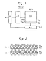
- Fig. 1 is a block diagram illustrating a general configuration of a PROM.
- the conventional PROM comprises a memory cell array MCA, a column decoder CD, a word decoder WD, and an address inverter Al.
- the memory cell array MCA comprises, in addition to usual memory cells MC, two test bit columns TB 1 and TB 2 , and the two test word rows TW ⁇ and TW 2 .
- the test bit columns TB 1 and TB 2 are illustrated in detail in Fig. 3.
- the test bit columns TB 1 and TB 2 comprises test memory cells.
- Each test memory cell is formed by, for example, a transistor. Originally, the test memory cells are at their nonconducting states. For the purpose of testing various functions of the PROM before shipment to a user, a test pattern is written into the test memory cells.
- Fig. 2 is an example of a test pattern to be written into the test memory cells.
- a blank square represents a data "0" and a hatched square represents a data "1".
- a test pattern of 011010011001011010 ... is sequentially inputted into the first test bit column TB I .
- the second test bit column TB 2 a test pattern inverted from the above test pattern is sequentially inputted.
- the arrangements of these test patterns are changed so that, as illustrated in Fig. 2(a), the first test bit column TB 1 comprises a test pattern of 101010..., and the second test bit column TB 2 comprises a test pattern of 010101 ....
- the numbers above or below the test patterns in Figs. 2(a) and 2(b) indicate the addresses of the memory cells.
- tests may be effected before the PROM is shipped from the manufacturer to a user. For example, there are tests to determine whether the memory cells will always output "1" or "0", test for short-circuits between lines, test for the current absorbing capability of the decoder driver, tests for the high reference potential of the output voltage, tests for the value of the output current, tests for delay time, and tests to determine whether the decoder operates normally or abnormally.
- test pattern of Fig. 2(a) into test memory cells in the test bit columns TB 1 and TB 2 , almost all of the above-mentioned test can be performed, as described in detail in published European Patent Application No. 0 011 974.
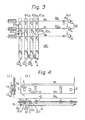
- Fig. 3 is a circuit diagram illustrating test memory cells in a PROM.
- memory cells MC are connected between bit lines B o , B 1' B 2' ... and word lines W o , W 1 , W 2 , ....
- One end of each bit line is connected to the corresponding output of the column decoder (Fig. 1), which provides a program signal when writing is effected.
- the other end of each bit line is connected through a diode D and a resistor R to a power supply line V cc for pulling up the bit line.
- the other end of each bit line is connected through the diode D and a corresponding inverter gate Go, G 1 , G 2 , ...
- the word lines W o , W 1 , W 2 , ... are connected through word-line selection transistors Q o , Q 1 , Q 2 , ... , respectively, to the ground.
- the outputs of the word decoder WD (Fig. 1) are connected to the bases of the corresponding transistors Q o , Q 1 , Q 2 , ..., so that these transistors Q o , Q 1 , Q2, ... are turned on or off depending on the outputs of the word decoder WD.
- each memory cell is formed by a base-opened npn transistor having an emitter connected to the corresponding bit line and a collector connected to the corresponding word line.
- the junction between the emitter and the base of each base-opened npn transistor is not broken so that all memory cells are in a nonconducting state.
- the word decoder WD provides a high potential output to turn on the corresponding transistor Q o , Q 1 , or Q 2 , ...
- the column decoder CD provides a program signal having a high potential output of about 20 V to the corresponding bit line.
- the bit lines B o and B 1 are included in the test bit columns TB 1 and TB 2 , respectively.
- the test pattern illustrated in Fig. 2(a) is written in the memory cells included in the test bit columns TB 1 and TB 2 .
- the test bit column TB 1 comprises alternately arranged nonconducting and conducting memory cells 10 ao , 10 io , 10 bo , 10 jo ,....
- the test bit column TB 2 comprises alternately arranged conducting and nonconducting memory cells 10 i1 , 10 a1' 10 j1 , 10 b1' ....
- the other memory cells connected between the bit lines B 2 , B 3 , ... and the word lines W o , W i , W 2 , ... are used as actual memory cells which are kept in the nonconducting state before the PROM is shipped to the user.
- Fig. 4(a) is a general plan view of the word line W o in a conventional PROM.
- Figs. 4(b) and 4(c) are general cross-sectional views taken along lines X-X and Y-Y, respectively of Fig. 4(a). Referring to Figs. 4(a) through 4(c), the memory cells 10 ao , 10 i1 , ...
- word lines W o are associated with the word line W o ; 12 represents a connecting portion between the word line W o and a buried layer 14; 16 represents isolation regions for electrically isolating adjacent word lines; 18 represents an n-type collector region; 200 and 201 represent p-type base regions formed in the collector region 18; and E o and E 1 represent n-type emitter regions formed in the base regions 200 and 201, respectively.
- the bit lines B o and B 1 are made in contact with the emitter regions E o and E 1' respectively.
- the column decoder CD selects one of the bit lines B o , B 1' ... to apply a write-in voltage of, for example 20 V, to the selected bit line; and the word decoder selects one of the transistors Q o , Q 1 , Q 2 , ... (Fig. 3) to turn it on.
- a breakdown will occur in the junction between the emitter and the base. For example, when the transistor 10 i1 (Fig. 1)
- the memory cell 10 a1 is a transistor with an emitter-base junction which constitutes a diode inserted in reverse polarity in the current path from the bit line B 1 to the word line W 1 . Therefore, the memory cell 10 a1 does not conduct a current from the bit line B 1 to the word line W 1 . Accordingly, the bit line B 1 is maintained at the high reference potential.
- the potentials at the bit lines B o , B 1 ' B 2' ... are inverted by the inverter gates Go, G i , G 2 , ... , respectively.
- the outputs of the inverter gates are the readout data.
- test pattern illustrated in Fig. 2 is written into the memory cells connected to the bit lines B o and B 1 in a similar way as described above. Various tests can be performed by using this test pattern.
- the resistance R 1 between the adjacent word lines W 1 and W 2 is decreased to a sufficiently low value.
- the test memory cell MC 1 connected between the bit line B 1 and the word line W 1 it is assumed that a write-in operation has been effected by the manufacturer. Then, assume that the user tries to effect a write-in operation regarding the test memory cell MC 2 connected between the same bit line B 1 and the word line W 2 adjacent to the word line W 1 . In this condition, the memory cell MC 1 is a diode.
- a write-in error may be caused.
- the resistance R 1 has been decreased to a sufficiently low value; and also assume that, with respect to the memory cell MC 3 connected between the bit line B 2 and the word line W i , a write-in operation has been effected. Then, assume that the user tries to effect a write-in operation regarding the memory cell MC 4 connected between the same bit line B 2 and the word line W 2 adjacent to the word line W i . Because a leakage current will also flow through the already written memory cell MC 3 , the word line W 1 , the resistance R 1' and the transistor Q 2 to the ground, a write-in error will also occur.
- the present invention is provided in which the accidental generation of writing errors due to poor resistance between two adjacent word lines is prevented.
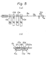
- Fig. 5(a) is a main portion of a circuit diagram of test memory cells according to an embodiment of the present invention.
- dotted square 10c, 10e, ... represent test memory cells into which write-in operations are not effected.
- Diodes 10d, 10f, ... represent test memory cells into which write-in operations are effected.
- the other portions are the same as those in the circuit of Fig. 3, and, therefore, are not described here.
- Fig. 5(b) is a cross-sectional view of the structure of two adjacent test memory cells 10c and 10d in Fig. 5(a). Referring to Fig. 5(b), the structure of the written-in test memory cell 10d is almost the same as the structure of the test memory cell 10ao illustrated in Fig. 4(c).
- the written-in test memory cell 10d comprises an n +- type buried layer 14d, an n-type collector region 18d formed on the buried layer 14d, a p-type base region 20d formed by diffusing acceptor atoms into the collector region 18d, an n-type emitter region 22d formed by diffusing donor atoms into the p-type base region 20d, an insulating film 24 covering these regions 18d, 20d, and 22d, and an aluminum evaporated film for the bit line Bo.
- a window is opened for contacting the emitter region 20d with the aluminum film.
- the nonwritten test memory cell 10c has no window in the insulating film 24.
- no emitter region is formed in the base region 20c of the memory cell 10c.
- the base region 20c is also unnecessary in the nonwritten memory cell 10c.
- the nonwritten test memory cells By forming the nonwritten test memory cells to have a structure as illustrated in Fig. 5(b), even application of a write-in voltage of more than 20 V to the bit line Bo will not cause leakage current flow from the aluminum evaporated film for the bit line Bo through the insulating film 24 to the collector region 18c, because there is a high insulating resistance and a high tolerance voltage between the bit line Bo and the collector region 18c due to the presence of the insulating film 24 between the bit line Bo and the collector region 18c.
- the above-mentioned non-current leakage characteristic between the test bit line and the collector region connected to the word line in a nonwritten memory cell can be used for testing insulation between two adjacent word lines.
- the non- written test memory cell 10bo has the same structure as that of the test memory cell 10c illustrated in Fig. 5(b). Even when the memory cell 10bo is selected by applying a write-in voltage of about 20 V to the bit line Bo and by turning on the transistor Q 2 , it can be assumed that a current does not flow from the bit line Bo to the word line W 2 because the insulating layer 24 entirely covers the transistor region of the memory cell 10bo.
- a current flowing through the word line W 2 is detected, it is considered that poor insulation is present between the word lines W 1 and W 2 or between the word lines W 2 and W 3 .
- a resistance R 1 between the word lines W 1 and W 2 a current will flow in the path from the bit line Bo through the written-in memory cell 10io, the word line W i , the resistance R,, and the word line W 2 to the transistor Q 2 .
- a resistance R 2 between the word lines W 2 and W 3 a current will flow in the path from the bit line Bo through the written-in memory cell 10jo, the word line W 3 , the resistance R 2 , and the word line W 2 to the transistor Q 2 .
- the value of the resistance R 1 or R 2 can be determined. If the value of the resistance between the two adjacent word lines is smaller than a predetermined limiting value, the insulation between the adjacent two word lines is determined as poor insulation.
- the PROM In the PROM, a number of wide-width word lines extend in parallel with a small gap between them, as illustrated partially in Fig. 4. Therefore, the possibility of poor insulation between adjacent word lines is relatively high. As described above, such poor insulation can be reliably determined by forming nonwritten memory cells in a test bit column as memory cells not connected to the bit line. While it is preferable to form non-written test memory cells which are not connected to respective bit lines, the present invention is not restricted to this: the test bit columns do not have to comprise nonwritten test memory cells, i.e., the nonwritten test memory cells do not have to be formed in the manufacturing step.
- transistor bits nonwritten memory cells
- diode bits written-in memory cells
- the poor insulation between adjacent word lines may be determined in a reading operation.
- the readout voltage applied to the bit line is sufficiently lower than the write-in voltage
- the leakage current flowing between the adjacent word lines is negligible.
- a small amount of leakage current will flow through the transistor bits.
- a high voltage nearly equal to the write-in voltage is applied to the bit lines, poor insulation may be determined by using the transistor bits and the diode bits. But, in this case, emitter-base breakdown in the transistor bits changes them to diode bits. Therefore, poor insulation between adjacent word lines cannot reliably be determined by using the transistor bits in a reading operation.
- the resistance between two adjacent word lines can be determined since the non-written memory cells in test bit columns are made as open bits. As a result a short circuit between adjacent word lines can be detected and the device rejected so preventing write-in errors occurring in the field.
- the present invention is not restricted to a PROM but may be applied to other field programmable devices, such as a ROM or FPLA.
Landscapes
- Read Only Memory (AREA)
- For Increasing The Reliability Of Semiconductor Memories (AREA)
- Testing Or Measuring Of Semiconductors Or The Like (AREA)
- Techniques For Improving Reliability Of Storages (AREA)
- Semiconductor Integrated Circuits (AREA)
- Semiconductor Memories (AREA)
Applications Claiming Priority (2)
| Application Number | Priority Date | Filing Date | Title |
|---|---|---|---|
| JP18229580A JPS57105898A (en) | 1980-12-23 | 1980-12-23 | Field programmable element |
| JP182295/80 | 1980-12-23 |
Publications (3)
| Publication Number | Publication Date |
|---|---|
| EP0055918A2 EP0055918A2 (en) | 1982-07-14 |
| EP0055918A3 EP0055918A3 (en) | 1982-08-04 |
| EP0055918B1 true EP0055918B1 (en) | 1985-11-21 |
Family
ID=16115780
Family Applications (1)
| Application Number | Title | Priority Date | Filing Date |
|---|---|---|---|
| EP81306060A Expired EP0055918B1 (en) | 1980-12-23 | 1981-12-22 | A field programmable semiconductor memory device |
Country Status (5)
| Country | Link |
|---|---|
| US (1) | US4459694A (enExample) |
| EP (1) | EP0055918B1 (enExample) |
| JP (1) | JPS57105898A (enExample) |
| DE (1) | DE3173031D1 (enExample) |
| IE (1) | IE52145B1 (enExample) |
Families Citing this family (22)
| Publication number | Priority date | Publication date | Assignee | Title |
|---|---|---|---|---|
| JPS59198596A (ja) * | 1983-04-22 | 1984-11-10 | Hitachi Micro Comput Eng Ltd | 検査回路 |
| JPS6095799A (ja) * | 1983-10-31 | 1985-05-29 | Nec Corp | プログラマブル・リ−ド・オンリ−・メモリ |
| JPS60109241A (ja) * | 1983-11-17 | 1985-06-14 | Fujitsu Ltd | 半導体装置の製造方法 |
| US4718042A (en) * | 1985-12-23 | 1988-01-05 | Ncr Corporation | Non-destructive method and circuit to determine the programmability of a one time programmable device |
| JPS62157400A (ja) * | 1985-12-27 | 1987-07-13 | Fujitsu Ltd | 半導体記憶回路 |
| US4731760A (en) * | 1986-05-05 | 1988-03-15 | Motorola, Inc. | On-chip test circuitry for an ECL PROM |
| EP0253161B1 (en) * | 1986-06-25 | 1991-10-16 | Nec Corporation | Testing circuit for random access memory device |
| US4801869A (en) * | 1987-04-27 | 1989-01-31 | International Business Machines Corporation | Semiconductor defect monitor for diagnosing processing-induced defects |
| JPS6425399A (en) * | 1987-07-21 | 1989-01-27 | Fujitsu Ltd | Programmable device and its test method |
| US5109353A (en) * | 1988-12-02 | 1992-04-28 | Quickturn Systems, Incorporated | Apparatus for emulation of electronic hardware system |
| US5329470A (en) * | 1988-12-02 | 1994-07-12 | Quickturn Systems, Inc. | Reconfigurable hardware emulation system |
| US5369593A (en) * | 1989-05-31 | 1994-11-29 | Synopsys Inc. | System for and method of connecting a hardware modeling element to a hardware modeling system |
| US5353243A (en) * | 1989-05-31 | 1994-10-04 | Synopsys Inc. | Hardware modeling system and method of use |
| JPH0754780A (ja) * | 1993-08-11 | 1995-02-28 | Paramount Bed Co Ltd | 供給エア圧可変型エアポンプ装置 |
| JPH0754781A (ja) * | 1993-08-11 | 1995-02-28 | Paramount Bed Co Ltd | 供給エア圧可変型エアポンプ装置 |
| US5680583A (en) * | 1994-02-16 | 1997-10-21 | Arkos Design, Inc. | Method and apparatus for a trace buffer in an emulation system |
| US5841967A (en) * | 1996-10-17 | 1998-11-24 | Quickturn Design Systems, Inc. | Method and apparatus for design verification using emulation and simulation |
| US5960191A (en) | 1997-05-30 | 1999-09-28 | Quickturn Design Systems, Inc. | Emulation system with time-multiplexed interconnect |
| US5970240A (en) * | 1997-06-25 | 1999-10-19 | Quickturn Design Systems, Inc. | Method and apparatus for configurable memory emulation |
| US6704677B2 (en) * | 2001-12-14 | 2004-03-09 | Sun Microsystems, Inc. | Method and apparatus for generating a data pattern for simultaneously testing multiple bus widths |
| US8959010B1 (en) | 2011-12-08 | 2015-02-17 | Cadence Design Systems, Inc. | Emulation system with improved reliability of interconnect and a method for programming such interconnect |
| US8743735B1 (en) | 2012-01-18 | 2014-06-03 | Cadence Design Systems, Inc. | Emulation system for verifying a network device |
Family Cites Families (9)
| Publication number | Priority date | Publication date | Assignee | Title |
|---|---|---|---|---|
| NL267532A (enExample) * | 1960-07-29 | |||
| US3995215A (en) * | 1974-06-26 | 1976-11-30 | International Business Machines Corporation | Test technique for semiconductor memory array |
| US4055802A (en) * | 1976-08-12 | 1977-10-25 | Bell Telephone Laboratories, Incorporated | Electrical identification of multiply configurable circuit array |
| JPS6027120B2 (ja) * | 1977-11-04 | 1985-06-27 | 日本電気株式会社 | プログラマブルメモリ |
| US4254477A (en) * | 1978-10-25 | 1981-03-03 | Mcdonnell Douglas Corporation | Reconfigurable memory circuit |
| EP0011974B1 (en) * | 1978-11-25 | 1984-02-15 | Fujitsu Limited | Programmable memory device provided with test means |
| JPS5914838B2 (ja) * | 1978-11-25 | 1984-04-06 | 富士通株式会社 | フィ−ルドプログラマブル素子 |
| US4301535A (en) * | 1979-07-02 | 1981-11-17 | Mostek Corporation | Programmable read only memory integrated circuit with bit-check and deprogramming modes and methods for programming and testing said circuit |
| US4389715A (en) * | 1980-10-06 | 1983-06-21 | Inmos Corporation | Redundancy scheme for a dynamic RAM |
-
1980
- 1980-12-23 JP JP18229580A patent/JPS57105898A/ja active Granted
-
1981
- 1981-12-22 DE DE8181306060T patent/DE3173031D1/de not_active Expired
- 1981-12-22 EP EP81306060A patent/EP0055918B1/en not_active Expired
- 1981-12-23 IE IE3063/81A patent/IE52145B1/en not_active IP Right Cessation
- 1981-12-23 US US06/333,653 patent/US4459694A/en not_active Expired - Lifetime
Also Published As
| Publication number | Publication date |
|---|---|
| DE3173031D1 (en) | 1986-01-02 |
| IE52145B1 (en) | 1987-07-08 |
| JPS6129079B2 (enExample) | 1986-07-04 |
| IE813063L (en) | 1982-06-23 |
| EP0055918A2 (en) | 1982-07-14 |
| US4459694A (en) | 1984-07-10 |
| EP0055918A3 (en) | 1982-08-04 |
| JPS57105898A (en) | 1982-07-01 |
Similar Documents
| Publication | Publication Date | Title |
|---|---|---|
| EP0055918B1 (en) | A field programmable semiconductor memory device | |
| KR910003147B1 (ko) | 반도체집적회로와 그 시험방법 | |
| US4723227A (en) | Redundant type memory circuit with an improved clock generator | |
| US3940740A (en) | Method for providing reconfigurable microelectronic circuit devices and products produced thereby | |
| US5392245A (en) | Redundancy elements using thin film transistors (TFTs) | |
| US4392211A (en) | Semiconductor memory device technical field | |
| KR930009544B1 (ko) | 정적형 반도체 기억 장치 | |
| US5132929A (en) | Static RAM including leakage current detector | |
| KR960013025B1 (ko) | 용장회로의 사용을 외부에서 용이하게 검출할 수 있는 반도체장치 및 반도체 메모리장치 | |
| EP0052481B1 (en) | Semiconductor device having a device state identifying circuit | |
| US4267583A (en) | Memory test device with write and pseudo write signals | |
| US5181205A (en) | Short circuit detector circuit for memory arrays | |
| US5610866A (en) | Circuit structure and method for stress testing of bit lines | |
| US4429388A (en) | Field programmable device with internal dynamic test circuit | |
| US4901284A (en) | Static random access memory | |
| US5629943A (en) | Integrated circuit memory with double bitline low special test mode control from output enable | |
| US4586170A (en) | Semiconductor memory redundant element identification circuit | |
| KR20050057585A (ko) | 자기저항 랜덤 액세스 메모리 내의 위크 비트들을 식별하기위한 방법 및 회로 | |
| US4465973A (en) | Pad for accelerated memory test | |
| JP4530527B2 (ja) | スタティック型半導体記憶装置 | |
| KR100258345B1 (ko) | 파워라인의 배치구조를 개선한 반도체 메모리 장치 | |
| US5577051A (en) | Static memory long write test | |
| EP0028157A1 (en) | Semiconductor integrated circuit memory device with integrated injection logic | |
| US3626390A (en) | Minimemory cell with epitaxial layer resistors and diode isolation | |
| JP2002093195A (ja) | 半導体記憶装置および半導体記憶装置のテスト方法 |
Legal Events
| Date | Code | Title | Description |
|---|---|---|---|
| PUAI | Public reference made under article 153(3) epc to a published international application that has entered the european phase |
Free format text: ORIGINAL CODE: 0009012 |
|
| PUAL | Search report despatched |
Free format text: ORIGINAL CODE: 0009013 |
|
| AK | Designated contracting states |
Designated state(s): DE FR GB NL |
|
| AK | Designated contracting states |
Designated state(s): DE FR GB NL |
|
| 17P | Request for examination filed |
Effective date: 19830113 |
|
| GRAA | (expected) grant |
Free format text: ORIGINAL CODE: 0009210 |
|
| AK | Designated contracting states |
Designated state(s): DE FR GB NL |
|
| REF | Corresponds to: |
Ref document number: 3173031 Country of ref document: DE Date of ref document: 19860102 |
|
| ET | Fr: translation filed | ||
| PLBE | No opposition filed within time limit |
Free format text: ORIGINAL CODE: 0009261 |
|
| STAA | Information on the status of an ep patent application or granted ep patent |
Free format text: STATUS: NO OPPOSITION FILED WITHIN TIME LIMIT |
|
| 26N | No opposition filed | ||
| PGFP | Annual fee paid to national office [announced via postgrant information from national office to epo] |
Ref country code: FR Payment date: 19971209 Year of fee payment: 17 |
|
| PGFP | Annual fee paid to national office [announced via postgrant information from national office to epo] |
Ref country code: GB Payment date: 19971215 Year of fee payment: 17 |
|
| PGFP | Annual fee paid to national office [announced via postgrant information from national office to epo] |
Ref country code: NL Payment date: 19971223 Year of fee payment: 17 |
|
| PGFP | Annual fee paid to national office [announced via postgrant information from national office to epo] |
Ref country code: DE Payment date: 19971230 Year of fee payment: 17 |
|
| PG25 | Lapsed in a contracting state [announced via postgrant information from national office to epo] |
Ref country code: GB Free format text: LAPSE BECAUSE OF NON-PAYMENT OF DUE FEES Effective date: 19981222 |
|
| PG25 | Lapsed in a contracting state [announced via postgrant information from national office to epo] |
Ref country code: NL Free format text: LAPSE BECAUSE OF NON-PAYMENT OF DUE FEES Effective date: 19990701 |
|
| GBPC | Gb: european patent ceased through non-payment of renewal fee |
Effective date: 19981222 |
|
| PG25 | Lapsed in a contracting state [announced via postgrant information from national office to epo] |
Ref country code: FR Free format text: LAPSE BECAUSE OF NON-PAYMENT OF DUE FEES Effective date: 19990831 |
|
| NLV4 | Nl: lapsed or anulled due to non-payment of the annual fee |
Effective date: 19990701 |
|
| REG | Reference to a national code |
Ref country code: FR Ref legal event code: ST |
|
| PG25 | Lapsed in a contracting state [announced via postgrant information from national office to epo] |
Ref country code: DE Free format text: LAPSE BECAUSE OF NON-PAYMENT OF DUE FEES Effective date: 19991001 |