EP0036859B1 - Boat for wafer processing - Google Patents
Boat for wafer processing Download PDFInfo
- Publication number
- EP0036859B1 EP0036859B1 EP80901301A EP80901301A EP0036859B1 EP 0036859 B1 EP0036859 B1 EP 0036859B1 EP 80901301 A EP80901301 A EP 80901301A EP 80901301 A EP80901301 A EP 80901301A EP 0036859 B1 EP0036859 B1 EP 0036859B1
- Authority
- EP
- European Patent Office
- Prior art keywords
- boat
- notches
- shaped
- bottom plate
- wafer
- Prior art date
- Legal status (The legal status is an assumption and is not a legal conclusion. Google has not performed a legal analysis and makes no representation as to the accuracy of the status listed.)
- Expired
Links
- 238000012545 processing Methods 0.000 title claims abstract description 16
- 235000012431 wafers Nutrition 0.000 claims abstract description 94
- 239000004065 semiconductor Substances 0.000 abstract description 15
- 238000005516 engineering process Methods 0.000 abstract description 5
- XUIMIQQOPSSXEZ-UHFFFAOYSA-N Silicon Chemical compound [Si] XUIMIQQOPSSXEZ-UHFFFAOYSA-N 0.000 description 8
- 229910052710 silicon Inorganic materials 0.000 description 8
- 239000010703 silicon Substances 0.000 description 8
- 239000000463 material Substances 0.000 description 6
- 238000004519 manufacturing process Methods 0.000 description 4
- 238000000034 method Methods 0.000 description 3
- 229910001218 Gallium arsenide Inorganic materials 0.000 description 2
- 238000001816 cooling Methods 0.000 description 2
- 238000009792 diffusion process Methods 0.000 description 2
- 230000003647 oxidation Effects 0.000 description 2
- 238000007254 oxidation reaction Methods 0.000 description 2
- 230000000284 resting effect Effects 0.000 description 2
- 229910052594 sapphire Inorganic materials 0.000 description 2
- 239000010980 sapphire Substances 0.000 description 2
- 235000002595 Solanum tuberosum Nutrition 0.000 description 1
- 244000061456 Solanum tuberosum Species 0.000 description 1
- 238000010521 absorption reaction Methods 0.000 description 1
- 238000003486 chemical etching Methods 0.000 description 1
- 239000011248 coating agent Substances 0.000 description 1
- 238000000576 coating method Methods 0.000 description 1
- 230000007423 decrease Effects 0.000 description 1
- 238000000151 deposition Methods 0.000 description 1
- 230000008021 deposition Effects 0.000 description 1
- 238000011161 development Methods 0.000 description 1
- 230000018109 developmental process Effects 0.000 description 1
- 239000002223 garnet Substances 0.000 description 1
- 239000007789 gas Substances 0.000 description 1
- 238000010438 heat treatment Methods 0.000 description 1
- 238000004518 low pressure chemical vapour deposition Methods 0.000 description 1
- 229920002120 photoresistant polymer Polymers 0.000 description 1
- 238000001020 plasma etching Methods 0.000 description 1
- 239000010453 quartz Substances 0.000 description 1
- 230000005855 radiation Effects 0.000 description 1
- 230000035939 shock Effects 0.000 description 1
- VYPSYNLAJGMNEJ-UHFFFAOYSA-N silicon dioxide Inorganic materials O=[Si]=O VYPSYNLAJGMNEJ-UHFFFAOYSA-N 0.000 description 1
- 238000006557 surface reaction Methods 0.000 description 1
- 238000012546 transfer Methods 0.000 description 1
- 238000004506 ultrasonic cleaning Methods 0.000 description 1
- XLYOFNOQVPJJNP-UHFFFAOYSA-N water Substances O XLYOFNOQVPJJNP-UHFFFAOYSA-N 0.000 description 1
Images


Classifications
-
- C—CHEMISTRY; METALLURGY
- C30—CRYSTAL GROWTH
- C30B—SINGLE-CRYSTAL GROWTH; UNIDIRECTIONAL SOLIDIFICATION OF EUTECTIC MATERIAL OR UNIDIRECTIONAL DEMIXING OF EUTECTOID MATERIAL; REFINING BY ZONE-MELTING OF MATERIAL; PRODUCTION OF A HOMOGENEOUS POLYCRYSTALLINE MATERIAL WITH DEFINED STRUCTURE; SINGLE CRYSTALS OR HOMOGENEOUS POLYCRYSTALLINE MATERIAL WITH DEFINED STRUCTURE; AFTER-TREATMENT OF SINGLE CRYSTALS OR A HOMOGENEOUS POLYCRYSTALLINE MATERIAL WITH DEFINED STRUCTURE; APPARATUS THEREFOR
- C30B31/00—Diffusion or doping processes for single crystals or homogeneous polycrystalline material with defined structure; Apparatus therefor
- C30B31/06—Diffusion or doping processes for single crystals or homogeneous polycrystalline material with defined structure; Apparatus therefor by contacting with diffusion material in the gaseous state
- C30B31/14—Substrate holders or susceptors
-
- C—CHEMISTRY; METALLURGY
- C30—CRYSTAL GROWTH
- C30B—SINGLE-CRYSTAL GROWTH; UNIDIRECTIONAL SOLIDIFICATION OF EUTECTIC MATERIAL OR UNIDIRECTIONAL DEMIXING OF EUTECTOID MATERIAL; REFINING BY ZONE-MELTING OF MATERIAL; PRODUCTION OF A HOMOGENEOUS POLYCRYSTALLINE MATERIAL WITH DEFINED STRUCTURE; SINGLE CRYSTALS OR HOMOGENEOUS POLYCRYSTALLINE MATERIAL WITH DEFINED STRUCTURE; AFTER-TREATMENT OF SINGLE CRYSTALS OR A HOMOGENEOUS POLYCRYSTALLINE MATERIAL WITH DEFINED STRUCTURE; APPARATUS THEREFOR
- C30B25/00—Single-crystal growth by chemical reaction of reactive gases, e.g. chemical vapour-deposition growth
- C30B25/02—Epitaxial-layer growth
- C30B25/12—Substrate holders or susceptors
Definitions
- the thermal expansion of one material is different from the other resulting in warping of the wafer into a shape much like a potato chip.
- the wafer warpage often exceeds the wafer breaking point and the constraints and pressures imposed on the designs of the prior art processing boats jam the wafers in a given position so that the wafers have a greater tendency to break as they warp during the fabrication process.
- the wafer breakage due to the thermal shock and warping is observed in the bulk silicon processing for NMOS, PMOS, CMOS or bipolar circuits.
- the front surface of the silicon wafers is polished to a mirror-like surface while the back side is merely lapped. These two surfaces also have two different thermal properties and the wafers warp during heating and cooling. Thus a certain wafer breakage rate is lower than the SOS wafers.
- Magnetic garnet wafers and GaAs wafers have a similar breakage problem as SOS wafers.
- US-A-40 53 294 discloses a semiconductor boat fabricated of stress relieved quartz bar having a rectangular cross section to elongate side bars and a parallel elongate lower bar are provided. A plurality of slots are formed on the inwardly facing corners of said side bars and the lower bar, so that groups of three slots lie in a common plane.
- the slots have a width for accepting a predetermined thickness of semi- conductor wafer and have beveled slot edges for facilitating the entry of the edges of the semiconductor wafers into said slots.
- the invention relates to a boat for holding wafers during processing as set forth in the first part of claim 1, and the invention is characterised by the features set forth in the second part of claim 1.
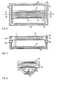
- FIG. 1 there is shown a perspective view of a boat 10 known in the prior art for holding wafers 11 typically composed of a semiconductor materials.
- the boat 10 is designed for holding a plurality of wafers 11 without touching during processing or circuit fabrication operations.
- semiconductor wafers are typically 5-10 cm (2-4 inches) in diameter, and about 0,3 to 0,6 mm (12 to 24 mils) in thickness.
- Each boat typically holds up to 25 wafers so that such wafers may be simultaneously subjected to processing.
- Examples of some of the processing operations to which the wafers may be subjected include oxidation, diffusion, LPCVD deposition, plasma etching, chemical etching, photoresist coating/baking/stripping, ultrasonic cleaning, as well as various automatic wafer handling operations.
- the application of wafer processing sequences is used in various semiconductor technologies including the fabrication of NMOS, PMOS, CMOS, SOS, bipolar, GaAs, and magnetic bubble memory devices.
- the boat shown in FIG. 1 consists of a first 12 and a second 13 bottom rod for holding the wafers in position in the boat.
- the bottom rods 12 and 13 are each provided with a corresponding plurality of parallel V-grooves 14 which are used to hold the wafer in a specific position.
- the V-grooves 14 are disposed along an arcuate portion of the bottom rods so as to contact a circumferential portion of the wafers in the boat.
- a first 15 and second 16 guide rail is disposed above the bottom rods 12 and 13 respectively.
- Corresponding V-grooves 17 are also provided in the rails 14 and 15 in a position essentially above the V-grooves 14 in the rods 12 and 13.
- the wafer has very little opportunity to wobble about any one of the contact points.
- various structural members of the boat 10 which function to provide rigidity to the structure and connect the bottom rods 12, 13 to the rails 15, 16.
- These members include a bottom support which is shown as consisting of two parallel rods 18 and 19 disposed parallel to the bottom rods 12 and 13.
- connecting bars 20 and 21 are provided which connect the ends of the rods 18 and 19.
- Four vertical supports 22, 23, 24, and 25 are provided which connect the ends of the rod 14 and rail 15, and rod 13 and rail 16, with the bottom support 18, 19.
- crossbars 27, 28, 29, and 30 are also provided. Such crossbars provide structural rigidity to the boat.
- the exterior side of the guide rail contains notches 31 and 34 disposed adjacent to the opposite ends of the tail, while the rail 16 contains similarly disposed notches 32 and 33.
- the function of such notches is to provide a location where the boat can be aligned by an external device for simultaneously transferring the wafers in the boat to another processing carrier.
- FIG. 2 there is shown a perspective view of a boat 35 according to the present invention for holding wafers 11.
- Many of the basic structural features found in the boat 10 are also present in the boat 35; like reference numerals have been used for such parts, including rods 18 and 19, connecting bars 20 and 21, vertical supports 22, 23, 24, and 25, and crossbars 27, 28, 29, and 30.
- the boat 35 includes a bottom plate 36 extending between connecting bars 20 and 21.
- the plate 36 is formed as a rectangularly shaped slab having a plurality of equally spaced substantially parallel V-groove notches 37 extending across the width of the upper major surface of the plate. Such V-groove notches extend parallel to the shorter edge of the plate, i.e. the edge abutting the connecting bars 20 and 21.
- the boat 35 further includes side rails 38 and 39 which are connected to the tops of the vertical supports, and the ends of the crossbars.
- the side rail 38 is disposed above, parallel to, and away from the rod 18, while the side rail 39 is disposed above, parallel to, and away from the rod 19.
- the side rails 38, 39 are rectangular plates having a plurality of U-shaped notches 40 on the interior side of the rail (i.e., the side facing the interior of the boat).
- the U-shaped notches 40 function to hold the opposite sides of the wafers 11 placed in the boat.
- the U-shaped notches 40 are parallel to one another and equally spaced, and extended from one end of the rail to the other.
- the bottom of the U-shaped notches 40 is substantially flat.
- Each of the U-shaped notches 40 correspond to a single one of the V-groove notches 37, so that a wafer 11 placed in one of the V-groove notches 37 will have its sides rest in the corresponding U-shaped notches 40.
- the U-shaped notches 40 are disposed in relation to the V-groove notches 37 so that an extension of one side of each of the U-shaped notches 40 falls closely adjacent to the line representing the extending of the apex line of the corresponding V-groove notch 37, as can be seen from FIG. 6.
- FIG. 6 shows the wafers 11 aligning in a near perfect parallel configuration.
- Such a configuration with substantially equal spacing between wafers, allows uniform flow of gases between the wafers, thereby permitting much more uniform oxidation, diffusion, or other surface reactions over the entire diameter of the wafer than in configurations according to the prior art.
- FIG. 7a is an enlarged top view of a boat according to the prior art with a semiconductor wafer placed therein which has warped.
- FIG. 7b is a top view of the boat according to the present invention as shown in FIG. 2 with a semiconductor wafer placed therein which has warped.
- the wafer 11 has much more room between the teeth 40, and even in its warped state, the wafer 11 is not pressed against the sides of the teeth 40. Morever, the single slot 27 in the bottom plate 36 (not shown) permits a far greater degree of freedom and movement of the wafer as it warps, so that a far smaller amount of stress is built up across the surface of the wafer. Therefore, there is a much smaller tendency for the wafers to shatter in the boat according to the present invention.
- V-groove notches in the bottom plate and the U-shaped notches are disposed with respect to one another so that a wafer placed in one of the V-groove notches and lying in a corresponding U-shaped notch is capable of pivoting at an angle of approximately five degrees around a fixed point in the apex of the said V-groove notch.
Landscapes
- Chemical & Material Sciences (AREA)
- Engineering & Computer Science (AREA)
- Crystallography & Structural Chemistry (AREA)
- Materials Engineering (AREA)
- Metallurgy (AREA)
- Organic Chemistry (AREA)
- Chemical Kinetics & Catalysis (AREA)
- General Chemical & Material Sciences (AREA)
- Container, Conveyance, Adherence, Positioning, Of Wafer (AREA)
- Coating Apparatus (AREA)
Applications Claiming Priority (2)
| Application Number | Priority Date | Filing Date | Title |
|---|---|---|---|
| US06/076,045 US4256229A (en) | 1979-09-17 | 1979-09-17 | Boat for wafer processing |
| US76045 | 1979-09-17 |
Publications (3)
| Publication Number | Publication Date |
|---|---|
| EP0036859A1 EP0036859A1 (en) | 1981-10-07 |
| EP0036859A4 EP0036859A4 (en) | 1982-02-05 |
| EP0036859B1 true EP0036859B1 (en) | 1984-05-02 |
Family
ID=22129605
Family Applications (1)
| Application Number | Title | Priority Date | Filing Date |
|---|---|---|---|
| EP80901301A Expired EP0036859B1 (en) | 1979-09-17 | 1981-03-23 | Boat for wafer processing |
Country Status (6)
| Country | Link |
|---|---|
| US (1) | US4256229A (OSRAM) |
| EP (1) | EP0036859B1 (OSRAM) |
| JP (1) | JPS56501225A (OSRAM) |
| CA (1) | CA1143074A (OSRAM) |
| DE (1) | DE3067677D1 (OSRAM) |
| WO (1) | WO1981000681A1 (OSRAM) |
Families Citing this family (46)
| Publication number | Priority date | Publication date | Assignee | Title |
|---|---|---|---|---|
| US4434899A (en) | 1980-11-17 | 1984-03-06 | Liberty Carton Co. | Adjustable wire tote for printed circuit boards |
| US4355974A (en) * | 1980-11-24 | 1982-10-26 | Asq Boats, Inc. | Wafer boat |
| US4518085A (en) * | 1982-04-29 | 1985-05-21 | At&T Technologies, Inc. | Multi-purpose transport tray |
| JPH0624199B2 (ja) * | 1982-07-30 | 1994-03-30 | 株式会社日立製作所 | ウエハの加工方法 |
| EP0100539A3 (en) * | 1982-07-30 | 1985-05-22 | Tecnisco Ltd. | Assembled device for supporting semiconductor wafers or the like |
| US5230747A (en) * | 1982-07-30 | 1993-07-27 | Hitachi, Ltd. | Wafer having chamfered bend portions in the joint regions between the contour of the wafer and the cut-away portion of the wafer |
| US5279992A (en) * | 1982-07-30 | 1994-01-18 | Hitachi, Ltd. | Method of producing a wafer having a curved notch |
| US4572101A (en) * | 1983-05-13 | 1986-02-25 | Asq Boats, Inc. | Side lifting wafer boat assembly |
| US4484538A (en) * | 1983-11-16 | 1984-11-27 | Btu Engineering Corporation | Apparatus for providing depletion-free uniform thickness CVD thin-film on semiconductor wafers |
| US4740249A (en) * | 1984-05-21 | 1988-04-26 | Christopher F. McConnell | Method of treating wafers with fluid |
| US4577650A (en) * | 1984-05-21 | 1986-03-25 | Mcconnell Christopher F | Vessel and system for treating wafers with fluids |
| US4633893A (en) * | 1984-05-21 | 1987-01-06 | Cfm Technologies Limited Partnership | Apparatus for treating semiconductor wafers |
| US4738272A (en) * | 1984-05-21 | 1988-04-19 | Mcconnell Christopher F | Vessel and system for treating wafers with fluids |
| DE3440111C1 (de) * | 1984-11-02 | 1986-05-15 | Heraeus Quarzschmelze Gmbh, 6450 Hanau | Traegerhorde |
| US4653636A (en) * | 1985-05-14 | 1987-03-31 | Microglass, Inc. | Wafer carrier and method |
| JPH0736418B2 (ja) * | 1986-05-19 | 1995-04-19 | 富士通株式会社 | ウエーハキャリア |
| EP0267462A3 (en) * | 1986-11-12 | 1990-01-31 | Heraeus Amersil, Inc. | Mass transferable semiconductor substrate processing and handling full shell carrier (boat) |
| US4949848A (en) * | 1988-04-29 | 1990-08-21 | Fluoroware, Inc. | Wafer carrier |
| US5111936A (en) * | 1990-11-30 | 1992-05-12 | Fluoroware | Wafer carrier |
| KR100254653B1 (ko) | 1991-10-04 | 2000-05-01 | 월터 알란 이. | 대상물을 처리하는 방법 |
| DE4428169C2 (de) * | 1994-08-09 | 1996-07-11 | Steag Micro Tech Gmbh | Träger für Substrate |
| US5785518A (en) * | 1994-09-30 | 1998-07-28 | Sony Corporation | Masking element fixture |
| US5772784A (en) * | 1994-11-14 | 1998-06-30 | Yieldup International | Ultra-low particle semiconductor cleaner |
| US5958146A (en) * | 1994-11-14 | 1999-09-28 | Yieldup International | Ultra-low particle semiconductor cleaner using heated fluids |
| USD381344S (en) * | 1995-07-31 | 1997-07-22 | Kaijo Corporation | Disk carrier |
| US6214127B1 (en) | 1998-02-04 | 2001-04-10 | Micron Technology, Inc. | Methods of processing electronic device workpieces and methods of positioning electronic device workpieces within a workpiece carrier |
| US6520191B1 (en) * | 1998-10-19 | 2003-02-18 | Memc Electronic Materials, Inc. | Carrier for cleaning silicon wafers |
| US6176377B1 (en) * | 1999-08-18 | 2001-01-23 | Ali Industries, Inc. | Rack for supporting abrasive discs or the like |
| WO2001096193A2 (en) * | 2000-06-12 | 2001-12-20 | Incyte Genomics, Inc. | Microscope slide container |
| US6455395B1 (en) * | 2000-06-30 | 2002-09-24 | Integrated Materials, Inc. | Method of fabricating silicon structures including fixtures for supporting wafers |
| US6871657B2 (en) * | 2001-04-06 | 2005-03-29 | Akrion, Llc | Low profile wafer carrier |
| JP2003201148A (ja) * | 2001-10-31 | 2003-07-15 | Nippon Sheet Glass Co Ltd | 情報記録媒体用ガラス基板の化学強化用ホルダー |
| KR100481855B1 (ko) * | 2002-08-05 | 2005-04-11 | 삼성전자주식회사 | 집적회로 제조 장치 |
| US6814808B1 (en) | 2002-10-08 | 2004-11-09 | Sci-Tech Glassblowing, Inc. | Carrier for semiconductor wafers |
| FR2846785B1 (fr) * | 2002-11-04 | 2005-02-04 | Soitec Silicon On Insulator | Nacelle de manutention de tranches de materiau semiconducteur |
| FR2858306B1 (fr) * | 2003-07-28 | 2007-11-23 | Semco Engineering Sa | Support de plaquettes, convertible pouvant recevoir au moins deux types de plaquettes differencies par la dimension des plaquettes. |
| KR100921521B1 (ko) * | 2007-10-12 | 2009-10-12 | 세메스 주식회사 | 기판 지지 유닛 및 이를 이용한 기판 처리 장치 |
| JP4999808B2 (ja) * | 2008-09-29 | 2012-08-15 | 東京エレクトロン株式会社 | 基板処理装置 |
| US20110062053A1 (en) * | 2009-07-13 | 2011-03-17 | Greene Tweed Of Delaware, Inc. | Chimerized Wafer Boat for Use in Semiconductor Chip Processing and Related Methods |
| US20120247686A1 (en) * | 2011-03-28 | 2012-10-04 | Memc Electronic Materials, Inc. | Systems and Methods For Ultrasonically Cleaving A Bonded Wafer Pair |
| DE202012005850U1 (de) | 2012-06-14 | 2012-10-10 | Institut Für Solarenergieforschung Gmbh | Vorrichtung zum Halten von Halbleitersubstraten verschiedener Formen und Größen |
| CN104992917B (zh) * | 2015-08-10 | 2018-04-24 | 乐山无线电股份有限公司 | 一种硅片载具 |
| CN107325324B (zh) * | 2016-04-28 | 2019-08-20 | 中国石油化工股份有限公司 | 阻燃剂、阻燃防静电组合物和阻燃防静电聚丙烯发泡珠粒 |
| CN206961808U (zh) * | 2017-07-14 | 2018-02-02 | 君泰创新(北京)科技有限公司 | 硅片清洗工装 |
| CN109637958B (zh) * | 2019-01-21 | 2024-02-20 | 苏州赛森电子科技有限公司 | 一种硅片腐蚀工艺固定载具及固定方法 |
| CN112831833B (zh) * | 2020-12-31 | 2024-04-09 | 中核北方核燃料元件有限公司 | 一种可定位的物料舟皿 |
Family Cites Families (10)
| Publication number | Priority date | Publication date | Assignee | Title |
|---|---|---|---|---|
| GB950052A (en) * | 1962-12-17 | 1964-02-19 | Upsala Ekeby Aktiebolag | Improvements in stands for supporting and transporting flat ceramic articles for firing the same |
| US3553037A (en) * | 1968-04-05 | 1971-01-05 | Stewart Warner Corp | Gas diffusion method for fabricating semiconductor devices |
| DE2133877A1 (de) * | 1971-07-07 | 1973-01-18 | Siemens Ag | Anordnung zum eindiffundieren von dotierstoffen in halbleiterscheiben |
| DE2133876A1 (de) * | 1971-07-07 | 1973-01-18 | Siemens Ag | Anordnung zum eindiffundieren von dotierstoffen |
| JPS5812730B2 (ja) * | 1973-08-06 | 1983-03-10 | 株式会社日立製作所 | ウエ−ハジグ |
| JPS5068775A (OSRAM) * | 1973-10-19 | 1975-06-09 | ||
| US3923156A (en) * | 1974-04-29 | 1975-12-02 | Fluoroware Inc | Wafer basket |
| US4053294A (en) * | 1976-05-19 | 1977-10-11 | California Quartzware Corporation | Low stress semiconductor wafer carrier and method of manufacture |
| US4098923A (en) * | 1976-06-07 | 1978-07-04 | Motorola, Inc. | Pyrolytic deposition of silicon dioxide on semiconductors using a shrouded boat |
| US4176751A (en) * | 1977-01-27 | 1979-12-04 | Northern Telecom Limited | Container apparatus for handling semiconductor wafers |
-
1979
- 1979-09-17 US US06/076,045 patent/US4256229A/en not_active Expired - Lifetime
-
1980
- 1980-06-06 JP JP50153080A patent/JPS56501225A/ja active Pending
- 1980-06-06 WO PCT/US1980/000706 patent/WO1981000681A1/en not_active Ceased
- 1980-06-06 DE DE8080901301T patent/DE3067677D1/de not_active Expired
- 1980-08-21 CA CA000358759A patent/CA1143074A/en not_active Expired
-
1981
- 1981-03-23 EP EP80901301A patent/EP0036859B1/en not_active Expired
Also Published As
| Publication number | Publication date |
|---|---|
| EP0036859A1 (en) | 1981-10-07 |
| WO1981000681A1 (en) | 1981-03-19 |
| CA1143074A (en) | 1983-03-15 |
| EP0036859A4 (en) | 1982-02-05 |
| DE3067677D1 (en) | 1984-06-07 |
| US4256229A (en) | 1981-03-17 |
| JPS56501225A (OSRAM) | 1981-08-27 |
Similar Documents
| Publication | Publication Date | Title |
|---|---|---|
| EP0036859B1 (en) | Boat for wafer processing | |
| US5948689A (en) | Integrated thermal coupling for heat generating device | |
| US7048488B1 (en) | Apparatus for transferring wafer and ring | |
| KR100530407B1 (ko) | 반도체 제조 장치 | |
| US5534074A (en) | Vertical boat for holding semiconductor wafers | |
| EP0793260A1 (en) | Vertical wafer boat | |
| KR100419812B1 (ko) | 열처리장치및공정 | |
| JPH05102056A (ja) | ウエハー支持具 | |
| KR20090034833A (ko) | 웨이퍼 플랫폼 | |
| KR20010041263A (ko) | 둥근 수평 아암을 갖는 슬립 가능한 수직형 래크 | |
| US6464445B2 (en) | System and method for improved throughput of semiconductor wafer processing | |
| US6331023B1 (en) | Gridded substrate transport spatula | |
| EP0164892B1 (en) | Horizontal furnace apparatus | |
| US7055702B1 (en) | Slip resistant horizontal semiconductor wafer boat | |
| CN110880466A (zh) | 晶片舟 | |
| US6582221B1 (en) | Wafer boat and method for treatment of substrates | |
| JPH0661331A (ja) | 基板搬送装置 | |
| JPH05235156A (ja) | 縦型炉用ボート | |
| KR200198430Y1 (ko) | 반도체에싱장비의웨이퍼이송용패들암 | |
| US5817179A (en) | GaAs anneal boat design and method for use | |
| KR19980016043A (ko) | 반도체설비의 웨이퍼 보트 거치용 로딩 덕트 | |
| KR19990079451A (ko) | 반도체 웨이퍼 캐리어 | |
| JPS59154017A (ja) | 半導体ウエハの加熱炉用パドル | |
| JPH05267202A (ja) | ウェーハ支持ボート | |
| JP2533551Y2 (ja) | 半導体ウエハ保持治具 |
Legal Events
| Date | Code | Title | Description |
|---|---|---|---|
| PUAI | Public reference made under article 153(3) epc to a published international application that has entered the european phase |
Free format text: ORIGINAL CODE: 0009012 |
|
| AK | Designated contracting states |
Designated state(s): DE FR GB |
|
| 17P | Request for examination filed |
Effective date: 19810911 |
|
| RBV | Designated contracting states (corrected) |
Designated state(s): DE FR GB |
|
| GRAA | (expected) grant |
Free format text: ORIGINAL CODE: 0009210 |
|
| AK | Designated contracting states |
Designated state(s): DE FR GB |
|
| REF | Corresponds to: |
Ref document number: 3067677 Country of ref document: DE Date of ref document: 19840607 |
|
| ET | Fr: translation filed | ||
| PG25 | Lapsed in a contracting state [announced via postgrant information from national office to epo] |
Ref country code: FR Free format text: LAPSE BECAUSE OF NON-PAYMENT OF DUE FEES Effective date: 19850228 |
|
| PG25 | Lapsed in a contracting state [announced via postgrant information from national office to epo] |
Ref country code: DE Effective date: 19850301 |
|
| PLBE | No opposition filed within time limit |
Free format text: ORIGINAL CODE: 0009261 |
|
| STAA | Information on the status of an ep patent application or granted ep patent |
Free format text: STATUS: NO OPPOSITION FILED WITHIN TIME LIMIT |
|
| REG | Reference to a national code |
Ref country code: FR Ref legal event code: ST |
|
| 26N | No opposition filed | ||
| GBPC | Gb: european patent ceased through non-payment of renewal fee | ||
| PG25 | Lapsed in a contracting state [announced via postgrant information from national office to epo] |
Ref country code: GB Effective date: 19881118 |