EP0030638B2 - Verfahren zur Abscheidung von Silizium oder Germanium enthaltenden Filmen - Google Patents
Verfahren zur Abscheidung von Silizium oder Germanium enthaltenden Filmen Download PDFInfo
- Publication number
- EP0030638B2 EP0030638B2 EP80107213A EP80107213A EP0030638B2 EP 0030638 B2 EP0030638 B2 EP 0030638B2 EP 80107213 A EP80107213 A EP 80107213A EP 80107213 A EP80107213 A EP 80107213A EP 0030638 B2 EP0030638 B2 EP 0030638B2
- Authority
- EP
- European Patent Office
- Prior art keywords
- film
- substrate
- gas
- deposition
- pressure
- Prior art date
- Legal status (The legal status is an assumption and is not a legal conclusion. Google has not performed a legal analysis and makes no representation as to the accuracy of the status listed.)
- Expired
Links
Images
Classifications
-
- H—ELECTRICITY
- H10—SEMICONDUCTOR DEVICES; ELECTRIC SOLID-STATE DEVICES NOT OTHERWISE PROVIDED FOR
- H10P—GENERIC PROCESSES OR APPARATUS FOR THE MANUFACTURE OR TREATMENT OF DEVICES COVERED BY CLASS H10
- H10P14/00—Formation of materials, e.g. in the shape of layers or pillars
- H10P14/60—Formation of materials, e.g. in the shape of layers or pillars of insulating materials
- H10P14/69—Inorganic materials
- H10P14/692—Inorganic materials composed of oxides, glassy oxides or oxide-based glasses
- H10P14/6921—Inorganic materials composed of oxides, glassy oxides or oxide-based glasses containing silicon
- H10P14/69215—Inorganic materials composed of oxides, glassy oxides or oxide-based glasses containing silicon the material being a silicon oxide, e.g. SiO2
-
- C—CHEMISTRY; METALLURGY
- C23—COATING METALLIC MATERIAL; COATING MATERIAL WITH METALLIC MATERIAL; CHEMICAL SURFACE TREATMENT; DIFFUSION TREATMENT OF METALLIC MATERIAL; COATING BY VACUUM EVAPORATION, BY SPUTTERING, BY ION IMPLANTATION OR BY CHEMICAL VAPOUR DEPOSITION, IN GENERAL; INHIBITING CORROSION OF METALLIC MATERIAL OR INCRUSTATION IN GENERAL
- C23C—COATING METALLIC MATERIAL; COATING MATERIAL WITH METALLIC MATERIAL; SURFACE TREATMENT OF METALLIC MATERIAL BY DIFFUSION INTO THE SURFACE, BY CHEMICAL CONVERSION OR SUBSTITUTION; COATING BY VACUUM EVAPORATION, BY SPUTTERING, BY ION IMPLANTATION OR BY CHEMICAL VAPOUR DEPOSITION, IN GENERAL
- C23C16/00—Chemical coating by decomposition of gaseous compounds, without leaving reaction products of surface material in the coating, i.e. chemical vapour deposition [CVD] processes
- C23C16/06—Chemical coating by decomposition of gaseous compounds, without leaving reaction products of surface material in the coating, i.e. chemical vapour deposition [CVD] processes characterised by the deposition of metallic material
-
- C—CHEMISTRY; METALLURGY
- C23—COATING METALLIC MATERIAL; COATING MATERIAL WITH METALLIC MATERIAL; CHEMICAL SURFACE TREATMENT; DIFFUSION TREATMENT OF METALLIC MATERIAL; COATING BY VACUUM EVAPORATION, BY SPUTTERING, BY ION IMPLANTATION OR BY CHEMICAL VAPOUR DEPOSITION, IN GENERAL; INHIBITING CORROSION OF METALLIC MATERIAL OR INCRUSTATION IN GENERAL
- C23C—COATING METALLIC MATERIAL; COATING MATERIAL WITH METALLIC MATERIAL; SURFACE TREATMENT OF METALLIC MATERIAL BY DIFFUSION INTO THE SURFACE, BY CHEMICAL CONVERSION OR SUBSTITUTION; COATING BY VACUUM EVAPORATION, BY SPUTTERING, BY ION IMPLANTATION OR BY CHEMICAL VAPOUR DEPOSITION, IN GENERAL
- C23C16/00—Chemical coating by decomposition of gaseous compounds, without leaving reaction products of surface material in the coating, i.e. chemical vapour deposition [CVD] processes
- C23C16/22—Chemical coating by decomposition of gaseous compounds, without leaving reaction products of surface material in the coating, i.e. chemical vapour deposition [CVD] processes characterised by the deposition of inorganic material, other than metallic material
- C23C16/24—Deposition of silicon only
-
- C—CHEMISTRY; METALLURGY
- C23—COATING METALLIC MATERIAL; COATING MATERIAL WITH METALLIC MATERIAL; CHEMICAL SURFACE TREATMENT; DIFFUSION TREATMENT OF METALLIC MATERIAL; COATING BY VACUUM EVAPORATION, BY SPUTTERING, BY ION IMPLANTATION OR BY CHEMICAL VAPOUR DEPOSITION, IN GENERAL; INHIBITING CORROSION OF METALLIC MATERIAL OR INCRUSTATION IN GENERAL
- C23C—COATING METALLIC MATERIAL; COATING MATERIAL WITH METALLIC MATERIAL; SURFACE TREATMENT OF METALLIC MATERIAL BY DIFFUSION INTO THE SURFACE, BY CHEMICAL CONVERSION OR SUBSTITUTION; COATING BY VACUUM EVAPORATION, BY SPUTTERING, BY ION IMPLANTATION OR BY CHEMICAL VAPOUR DEPOSITION, IN GENERAL
- C23C16/00—Chemical coating by decomposition of gaseous compounds, without leaving reaction products of surface material in the coating, i.e. chemical vapour deposition [CVD] processes
- C23C16/22—Chemical coating by decomposition of gaseous compounds, without leaving reaction products of surface material in the coating, i.e. chemical vapour deposition [CVD] processes characterised by the deposition of inorganic material, other than metallic material
- C23C16/30—Deposition of compounds, mixtures or solid solutions, e.g. borides, carbides, nitrides
- C23C16/32—Carbides
-
- C—CHEMISTRY; METALLURGY
- C23—COATING METALLIC MATERIAL; COATING MATERIAL WITH METALLIC MATERIAL; CHEMICAL SURFACE TREATMENT; DIFFUSION TREATMENT OF METALLIC MATERIAL; COATING BY VACUUM EVAPORATION, BY SPUTTERING, BY ION IMPLANTATION OR BY CHEMICAL VAPOUR DEPOSITION, IN GENERAL; INHIBITING CORROSION OF METALLIC MATERIAL OR INCRUSTATION IN GENERAL
- C23C—COATING METALLIC MATERIAL; COATING MATERIAL WITH METALLIC MATERIAL; SURFACE TREATMENT OF METALLIC MATERIAL BY DIFFUSION INTO THE SURFACE, BY CHEMICAL CONVERSION OR SUBSTITUTION; COATING BY VACUUM EVAPORATION, BY SPUTTERING, BY ION IMPLANTATION OR BY CHEMICAL VAPOUR DEPOSITION, IN GENERAL
- C23C16/00—Chemical coating by decomposition of gaseous compounds, without leaving reaction products of surface material in the coating, i.e. chemical vapour deposition [CVD] processes
- C23C16/22—Chemical coating by decomposition of gaseous compounds, without leaving reaction products of surface material in the coating, i.e. chemical vapour deposition [CVD] processes characterised by the deposition of inorganic material, other than metallic material
- C23C16/30—Deposition of compounds, mixtures or solid solutions, e.g. borides, carbides, nitrides
- C23C16/34—Nitrides
-
- C—CHEMISTRY; METALLURGY
- C23—COATING METALLIC MATERIAL; COATING MATERIAL WITH METALLIC MATERIAL; CHEMICAL SURFACE TREATMENT; DIFFUSION TREATMENT OF METALLIC MATERIAL; COATING BY VACUUM EVAPORATION, BY SPUTTERING, BY ION IMPLANTATION OR BY CHEMICAL VAPOUR DEPOSITION, IN GENERAL; INHIBITING CORROSION OF METALLIC MATERIAL OR INCRUSTATION IN GENERAL
- C23C—COATING METALLIC MATERIAL; COATING MATERIAL WITH METALLIC MATERIAL; SURFACE TREATMENT OF METALLIC MATERIAL BY DIFFUSION INTO THE SURFACE, BY CHEMICAL CONVERSION OR SUBSTITUTION; COATING BY VACUUM EVAPORATION, BY SPUTTERING, BY ION IMPLANTATION OR BY CHEMICAL VAPOUR DEPOSITION, IN GENERAL
- C23C16/00—Chemical coating by decomposition of gaseous compounds, without leaving reaction products of surface material in the coating, i.e. chemical vapour deposition [CVD] processes
- C23C16/22—Chemical coating by decomposition of gaseous compounds, without leaving reaction products of surface material in the coating, i.e. chemical vapour deposition [CVD] processes characterised by the deposition of inorganic material, other than metallic material
- C23C16/30—Deposition of compounds, mixtures or solid solutions, e.g. borides, carbides, nitrides
- C23C16/40—Oxides
- C23C16/401—Oxides containing silicon
- C23C16/402—Silicon dioxide
-
- H—ELECTRICITY
- H10—SEMICONDUCTOR DEVICES; ELECTRIC SOLID-STATE DEVICES NOT OTHERWISE PROVIDED FOR
- H10P—GENERIC PROCESSES OR APPARATUS FOR THE MANUFACTURE OR TREATMENT OF DEVICES COVERED BY CLASS H10
- H10P14/00—Formation of materials, e.g. in the shape of layers or pillars
- H10P14/20—Formation of materials, e.g. in the shape of layers or pillars of semiconductor materials
- H10P14/24—Formation of materials, e.g. in the shape of layers or pillars of semiconductor materials using chemical vapour deposition [CVD]
-
- H—ELECTRICITY
- H10—SEMICONDUCTOR DEVICES; ELECTRIC SOLID-STATE DEVICES NOT OTHERWISE PROVIDED FOR
- H10P—GENERIC PROCESSES OR APPARATUS FOR THE MANUFACTURE OR TREATMENT OF DEVICES COVERED BY CLASS H10
- H10P14/00—Formation of materials, e.g. in the shape of layers or pillars
- H10P14/20—Formation of materials, e.g. in the shape of layers or pillars of semiconductor materials
- H10P14/29—Formation of materials, e.g. in the shape of layers or pillars of semiconductor materials characterised by the substrates
- H10P14/2901—Materials
- H10P14/2921—Materials being crystalline insulating materials
-
- H—ELECTRICITY
- H10—SEMICONDUCTOR DEVICES; ELECTRIC SOLID-STATE DEVICES NOT OTHERWISE PROVIDED FOR
- H10P—GENERIC PROCESSES OR APPARATUS FOR THE MANUFACTURE OR TREATMENT OF DEVICES COVERED BY CLASS H10
- H10P14/00—Formation of materials, e.g. in the shape of layers or pillars
- H10P14/20—Formation of materials, e.g. in the shape of layers or pillars of semiconductor materials
- H10P14/34—Deposited materials, e.g. layers
- H10P14/3402—Deposited materials, e.g. layers characterised by the chemical composition
- H10P14/3404—Deposited materials, e.g. layers characterised by the chemical composition being Group IVA materials
- H10P14/3411—Silicon, silicon germanium or germanium
-
- H—ELECTRICITY
- H10—SEMICONDUCTOR DEVICES; ELECTRIC SOLID-STATE DEVICES NOT OTHERWISE PROVIDED FOR
- H10P—GENERIC PROCESSES OR APPARATUS FOR THE MANUFACTURE OR TREATMENT OF DEVICES COVERED BY CLASS H10
- H10P14/00—Formation of materials, e.g. in the shape of layers or pillars
- H10P14/20—Formation of materials, e.g. in the shape of layers or pillars of semiconductor materials
- H10P14/34—Deposited materials, e.g. layers
- H10P14/3438—Doping during depositing
- H10P14/3441—Conductivity type
- H10P14/3444—P-type
-
- H—ELECTRICITY
- H10—SEMICONDUCTOR DEVICES; ELECTRIC SOLID-STATE DEVICES NOT OTHERWISE PROVIDED FOR
- H10P—GENERIC PROCESSES OR APPARATUS FOR THE MANUFACTURE OR TREATMENT OF DEVICES COVERED BY CLASS H10
- H10P14/00—Formation of materials, e.g. in the shape of layers or pillars
- H10P14/60—Formation of materials, e.g. in the shape of layers or pillars of insulating materials
- H10P14/63—Formation of materials, e.g. in the shape of layers or pillars of insulating materials characterised by the formation processes
- H10P14/6326—Deposition processes
- H10P14/6328—Deposition from the gas or vapour phase
- H10P14/6334—Deposition from the gas or vapour phase using decomposition or reaction of gaseous or vapour phase compounds, i.e. chemical vapour deposition
- H10P14/6336—Deposition from the gas or vapour phase using decomposition or reaction of gaseous or vapour phase compounds, i.e. chemical vapour deposition in the presence of a plasma [PECVD]
-
- H—ELECTRICITY
- H10—SEMICONDUCTOR DEVICES; ELECTRIC SOLID-STATE DEVICES NOT OTHERWISE PROVIDED FOR
- H10P—GENERIC PROCESSES OR APPARATUS FOR THE MANUFACTURE OR TREATMENT OF DEVICES COVERED BY CLASS H10
- H10P14/00—Formation of materials, e.g. in the shape of layers or pillars
- H10P14/60—Formation of materials, e.g. in the shape of layers or pillars of insulating materials
- H10P14/66—Formation of materials, e.g. in the shape of layers or pillars of insulating materials characterised by the type of materials
- H10P14/668—Formation of materials, e.g. in the shape of layers or pillars of insulating materials characterised by the type of materials the materials being characterised by the deposition precursor materials
- H10P14/6681—Formation of materials, e.g. in the shape of layers or pillars of insulating materials characterised by the type of materials the materials being characterised by the deposition precursor materials the precursor containing a compound comprising Si
- H10P14/6682—Formation of materials, e.g. in the shape of layers or pillars of insulating materials characterised by the type of materials the materials being characterised by the deposition precursor materials the precursor containing a compound comprising Si the compound being a silane, e.g. disilane, methylsilane or chlorosilane
-
- H—ELECTRICITY
- H10—SEMICONDUCTOR DEVICES; ELECTRIC SOLID-STATE DEVICES NOT OTHERWISE PROVIDED FOR
- H10P—GENERIC PROCESSES OR APPARATUS FOR THE MANUFACTURE OR TREATMENT OF DEVICES COVERED BY CLASS H10
- H10P14/00—Formation of materials, e.g. in the shape of layers or pillars
- H10P14/60—Formation of materials, e.g. in the shape of layers or pillars of insulating materials
- H10P14/68—Organic materials, e.g. photoresists
-
- H—ELECTRICITY
- H10—SEMICONDUCTOR DEVICES; ELECTRIC SOLID-STATE DEVICES NOT OTHERWISE PROVIDED FOR
- H10P—GENERIC PROCESSES OR APPARATUS FOR THE MANUFACTURE OR TREATMENT OF DEVICES COVERED BY CLASS H10
- H10P14/00—Formation of materials, e.g. in the shape of layers or pillars
- H10P14/60—Formation of materials, e.g. in the shape of layers or pillars of insulating materials
- H10P14/69—Inorganic materials
- H10P14/6903—Inorganic materials containing silicon
- H10P14/6905—Inorganic materials containing silicon being a silicon carbide or silicon carbonitride and not containing oxygen, e.g. SiC or SiC:H
Definitions
- the invention relates to a method for depositing on a substrate silicon or germanium containing films by means of chemical vapor deposition.
- a semiconductor film may be deposited on the surface of a substrate to produce useful semiconducting devices such as diodes, solar cells and transistors.
- useful semiconducting devices such as diodes, solar cells and transistors.
- doped amorphous silicon layers that are produced from glow discharge plasmas of monosilane SiH 4 may be deposited so as to form PN junctions with useful electrical rectification characteristics.
- other potential applications for deposited silicon films are known to those skilled in the art.
- an amorphous silicon semiconducting film may be formed on a substrate by a capacitive glow discharge in a monosilane (SiH 4 ) gas. It is further indicated that the amorphous silicon film that is produced possesses characteristics that are ideally suited for a photovoltaic device and that are superior to the characteristics of a crystalline silicon film. For example, the optical absorption of the amorphous silicon is superior to the absorption of single crystalline silicon over the visible light range. Also, the electron lifetime in amorphous silicon that is produced by the glow discharge method is substantially longer than the electron lifetime of amorphous silicon that is formed by either sputtering or evaporation.
- the deposition parameters of a chemical vapor deposition process determine the rate at which a material is deposited on a substrate. More particularly, it has been determined that, in general, the rate of deposition will be increased if the pressure is increased during the deposition process. Thus, if it is necessary to reduce the pressure to produce a particular deposition product, as is suggested in Carlson, the reduced pressure will result in a corresponding reduced rate of deposition and an associated decrease in the efficiency of the deposition process.
- the slow rate of deposition also, apparently, causes a strain to appear at the interface between the deposited film and the supporting substrate.
- the strain tends to warp or distort the substrate and also limits the thickness of the film that may be deposited on the substrate.
- a reduced rate of deposition often results in the deposition of a film that has a rather rough surface, since the slow rate of deposition makes the deposition process more sensitive to physical factors that operate to vary the rate of growth at different locations on the substrate.
- the roughness of the film increases the probability that the film will break down in response to applied operational voltage and, also, the rough surface may cause nonuniform electrical fields to be produced if the film is employed in a semiconductor device.
- amorphous silicon nitride films have desirable insulating or protective properties and may be produced if a particular, relatively low temperature range is maintained during the glow discharge process. It is further indicated that as the deposition temperature rises outside the accepted range, the film becomes increasingly crystalline, thereby losing the favorable properties associated with an amorphous structure.
- insulating or protective films may be deposited in accordance with the Androshuk process at a relatively high pressure of from 0.133 to 13.33 mbar and, if an amorphous silicon nitride film is desired, a relatively low deposition temperature must be maintained.
- the deposition pressure and power have been maintained at relatively low levels in order to provide superior semiconducting properties for a deposited film.
- lower deposition pressures tend to slow down the rate. of deposition and thereby decrease the efficiency of the deposition process.
- the object of the invention is to provide a method of rapidly depositing on a substrate silicon or germanium containing film having superior photoelectric, semiconducting or other electrical properties and a smooth surface, and being characterised by a reduced or by no strain at the interface between film and substrate.
- the inventive method allows to form the films or layers on the substrate in response to relatively low temperature and pressure and a relatively low excitation power.
- the method overcomes the problems of the prior art.
- the gas atmosphere is preferably excited either thermally or by means of UV or laser irradiation or where a glow discharge is generated by RF inductive coupling, by RF capacitive coupling or by DC voltages,
- the excitation energy isapplied for example by activating an RF coil to inductively coupled RF energy, generating the glow discharge in that deposition gas or gas mixture which flows through the chemical vapor deposition apparatus by means of a gas inlet pipe and an associated gas outlet pipe connected to a vacuum pump.
- the inventive method is used to form a film of hydrogenated, amorphous silicon where the hydrogen content in the film is controlled by means of the gas pressure and the substrate temperature.
- a chemical vapor deposition apparatus for exciting a plasma comprised of a higher order silane gas in a volume adjacent to the surface of the heated substrate.
- the at least one gas reacting with the silane or the germane contains an element selected from the group oxygen, nitrogen, carbon and boron.
- the gas reacting with the silane or the germane may be carbon dioxide (C0 2 ), ammonia (NH 3 ), methane (CH 4 ) or diborane (B 2 H,).
- the deposited films contain silicon or germanium respectively and oxygen, nitrogen, carbon or boron and if desired hydrogen.
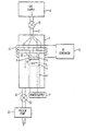
- FIG. 1 shows a diagrammatic view of an apparatus for depositing a film on a substrate by RF inductive coupling to a glow discharge in a disilane or a higher order silane gas.
- a reaction chamber 1 made of, for example quartz, contains a pedestal 3, preferably made of a heat conducting material such as aluminum, copper or carbon.
- a resistive heating element 5 is embedded in the pedestal 3 and is energized by a power supply 7 to heat the pedestal 3 to a desired deposition temperature.
- the pedestal 3 is supported by a support column 4, preferably made of a heat insulating material such as quartz or thin-wall stainless steel.
- the pedestal 3 and support 4 may be coated with a material such as nickel which is chemically resistant to the plasma gases of the apparatus.
- a substrate 9 is supported on the pedestal 3 and is held in position by clamps 11.
- the substrate 9 may be made in any suitable substrate material that is known in the semiconductor art, for example quartz, sapphire (AI 2 0 s ), metals or transparent metal films and semiconductors. However, a metal or metallized substrate is preferred for use in the process of the invention.
- a radio frequency (RF) coil 13 is disposed around the reaction chamber 1 and is connected to an RF generator 15 to inductively apply RF power to a region adjacent to the surface of the substrate 9.
- An input line 17 having a valve 18 connects a gas supply 19 to the interior of the reaction chamber and an outlet line 21 and associated valve 22 connect a vacuum pump 23 with the interior of the reaction chamber 1.
- the RF coil 13 forms a glow discharge adjacent to the surface of the substrate 9 and the gas supply 19 passes a deposition gas or gases at a pressure that is sufficient to form a plasma in the region of the glow discharge and to deposit a film 10 on the exposed surface of the substrate.
- the gas supply 19 is operated to supply disilane gas (Si2Hf,) to the reaction chamber 1.
- the disilane gas may be produced by passing monosilane (SiH 4 ) gas through a separate glow discharge apparatus and then employing known separation techniques, for example distillation, to remove disilane from the reaction products.
- the disilane gas may then be supplied to the reaction chamber by the inlet pipe 17 to produce a film of hydrogenated amorphous silicon.
- the disilane gas that does not react may be removed by the outlet pipe 21 and vented, collected for reuse or recirculated to the inlet pipe 17. It should be understood that other synthetic chemical techniques may be used to produce the disilane, without departing from the invention.
- the deposition process for the preferred embodiment of the invention is initiated by operating the vacuum pump 23 to evacuate the reaction chamber 1 to a pressure of less than 1.33.10-3 mbar.
- the power supply 7 is turned on to energize the resistive heating element 5 and to thereby heat the substrate 9 to a particular reaction temperature. If it is desired to deposit a layer of hydrogenated amorphous silicon on the substrate 9, the substrate 9 may be heated to a temperature within the range of 200°C to 350°C. Higher temperatures may be used to produce crystalline silicon films, if desired.
- the disilane gas from the gas supply 19 is supplied to the reaction chamber 1 through the inlet pipe 17 and the vacuum pump 23 is continuously operated to provide a flow of gas at a pressure of less than 0.133 mbar, depending upon the desired deposition rate and desired film properties.
- the RF generator 15 and associated RF coil 13 operate to inductively couple RF power to a glow discharge region that is adjacent to the surface of the substrate 9.
- the induced RF excitation power produces a glow discharge in the region and, once the glow discharge is initiated, hydrogenated amorphous silicon is deposited on the substrate 9. It has been experimentally determined that for a 76,2 mm RF coil and a pedestal of approximately 31.7 mm. and RF signal of 1 W and 13.56 MHz is sufficient to sustain a glow discharge in a disilane gas at the indicated pressure.
- Monohydrogenated amorphous silicon is differentiated from the more general hydrogenated amorphous silicon by the local chemical bonding environment of the hydrogen atoms.
- the hydrogen is predominantly bonded to silicon atoms which have their other three bonds connected to other silicon atoms.
- hydrogenated amorphous silicon can have a significant fraction of its hydrogen atoms bonded to silicon atoms in local environments wherein at least two hydrogen atoms are bonded to the same silicon atom. It will be understood by those skilled in the art that monohydrogenated amorphous silicon is now thought to be the most desirable hydrogenated material for semiconductor films.
- the monohydrogenated silicon that is produced in accordance with the method of the invention is characterized by approximately 85 atomic percent of silicon and 15 atomic percent of hydrogen for a 250°C substrate temperature and a 0.093 mbar pressure. For other temperatures and pressures within the indicated range, a different hydrogen content may result. In general, it should be understood that the invention is not limited to a particular hydrogen content for the deposited hydrogenated silicon.
- the temperature is maintained below the indicated high temperature level to avoid an excessive loss of hydrogen during the deposition process and to prevent the silicon film from crystallizing.
- the temperature is maintained above the indicated low temperature level to ensure that residual defects in the film are minimized and to avoid the formation of dihydride groups that, apparently, form at lower temperatures.
- a monohydrogenated amorphous silicon film by aglow discharge in a monosilane (SiH 4 ) gas.
- a glow discharge process is disclosed, for example, in the U.S. Patent to Carlson, No. 4 064 521.
- a glow discharge of monosilane gas is performed at the above-indicated temperature, pressure and RF power, a monohydrogenated silicon film will be formed relatively slowly, while if the same parameters are applied for a glow discharge in a disilane gas, the monohydrogenated silicon film will be produced much more rapidly.
- Amorphous silicon films have been experimentally deposited by the disilane glow discharge process of the invention and the monosilane glow discharge process of the prior art on substrates of quartz, sapphire, crystalline silicon and a metallized substance coated with molybdenum. It has been determined on the basis of the experimental depositions that the rate of growth of the film in the disilane process of the invention is approximately 25 times the rate of growth of the film in the prior art process. Also, the photo-conductivity of the experimental amorphous silicon films of the disilane process was higher than the photo-conductivity of the films of the prior art monosilane process. However, it is not understood at the present time if the increased photo-conductivity is due to the use of disilane per se or is related to the process by which the disilane is prepared.
- the disilane deposition process of the invention was applied within a temperature range of 250°C to 350°C'to produce a Schottky barrier photovoltaic solar cell having the structure described in the U.S. Patent to Carlson et al, No. 4 142 195.
- the solar cell that was produced by the process of the invention has a response that is at least as good as the response of a control solar cell that was produced within the indicated temperature range in accordance with a prior art monosilane deposition process.
- the deposition rate for the solar cell of the invention was much greater than the deposition rate for the solar cell that was produced in accordance with the prior art process.
- the glow discharge of monosilane tends to produce semiconducting films that have somewhat rough surfaces, particularly if a substrate such as sapphire (A1 2 0 3 ) is employed at the higher end of the indicated temperature range of 200°C to 350°C.
- the rough surface of the film increases the probability that the film will break down when subjected to typical semiconductor voltages, Moreover, the rough film may also cause nonuniform electric fields to be generated during a semiconductor operation.
- the process of the invention tends to produce hydrogenated amorphous silicon films that are very smooth, particularly if the film is deposited on a quartz substrate. It is theorized that the silane glow discharge process of the invention produces smooth film surfaces due to the rapid and, hence, uniform growth of the film.
- a trisilane gas Si 3 H 8
- Trisilane was employed in the deposition process of the invention and was found to further increase the deposition rate of hydrogenated silicon by a factor of two over the disilane process or by a factor of 50 over the monosilane process.
- higher order silanes may be employed in the process of the invention.
- disilane or higher order silanes may be reacted with additional reaction gases to deposit semiconducting or insulating films of a different composition.
- additional reaction gases For example, if ammonia gas is reacted with disilane or a higher order silane in a glow discharge process, a hydrogenated silicon nitride film will be deposited on an associated substrate.
- carbon dioxide may be reacted with disilane or a higher order silane to rapidly deposit a film of silicon dioxide on an underlying substrate, in accordance with the invention.
- acetylene C 2 H 2
- disilane or higher order silanes to rapidly deposit a film of a hydrogenated alloy of silicon and carbon.
- diborane B 2 H s
- B 2 H s may be reacted to produce a hydrogenated alloy or compound of silicon and boron.
- reacting gases for example nitrogen, oxygen, methane or other hydrocarbons or higher order boranes may be reacted with disilane or a higher order silane, without departing from the spirit of the invention.
- reacting gases for example nitrogen, oxygen, methane or other hydrocarbons or higher order boranes
- disilane or a higher order silane may be employed to achieve the improved deposition results of the invention.
- monosilane may be combined with a higher order silane or various higher order silanes may be combined to achieve a rapid deposition rate, in accordance with the invention.
- the process of the invention may be employed to rapidly deposit semiconducting or insulating films on a substrate, while utilizing a lower pressure, temperature and/ or excitation power. Accordingly, if for example a deposited film is sensitive to ultraviolet or other emissions from the plasma, the film may be rapidly produced in accordance with the invention with a relatively low level of radiation damage. Also, the process of the invention is carried out at the relatively low pressure of less than 0.133 mbar and, therefore, the process is distinguished from prior art processes that require films at slower growth rates.
- the lower pressures and powers of the process of the invention make it possible to consistently and rapidly produce hydrogenated amorphous silicon films having favorable photo- electronic and semiconductor properties.
- the relatively high levels of pressure and/or power that are required to increase the rate of deposition tend to cause the deposited film to have defects and to thereby lose some of its favorable semiconductor properties. Accordingly, it should be appreciated that in any deposition or reaction process wherein the decomposition of either monosilane or monogermane is a rate-limiting step in the process, disilane or a higher order silane or digermane or a higher order' germane may be employed to achieve the improved deposition results of the invention.
- the process of the invention is used to deposit an amorphous insulating or semiconducting film containing silicon or germanium, it is expected that higher deposition rates will be provided for lower temperatures and pressures. If lower deposition temperatures and pressures are maintained, the crystallization that is known to occur with higher substrate temperatures may be avoided.
- chemical vapor deposition method is intended to encompass all known processes for depositing a solid substance from a gas input, including processes wherein a glow discharge plasma of the input gas or gases is employed to deposit a substance.
- a glow discharge plasma may be excited by any method known to the art, for example by RF inductive coupling, RF capacitive coupling or by DC voltages.
- input gases may be thermally excited to provide a pyrolytic decomposition and/or reaction to achievethe results of the invention, without departing from the invention.
- Ultra-violet or laser excited chemical vapor processes also fall within the scope of the invention.
- the claimed deposition process may be employed to rapidly form insulating or semiconductive films for semiconducting devices such as diodes, solar cells and transistors.
- semiconducting devices such as diodes, solar cells and transistors.
- hydrogenated amorphous silicon films may be rapidly grown on a substrate in a relatively low temperature and pressure environment. The rapid growth of the films increases the efficiency of the process for manufacturing semiconductors.
Landscapes
- Chemical & Material Sciences (AREA)
- General Chemical & Material Sciences (AREA)
- Chemical Kinetics & Catalysis (AREA)
- Engineering & Computer Science (AREA)
- Materials Engineering (AREA)
- Mechanical Engineering (AREA)
- Metallurgy (AREA)
- Organic Chemistry (AREA)
- Inorganic Chemistry (AREA)
- Photovoltaic Devices (AREA)
Claims (9)
Applications Claiming Priority (2)
| Application Number | Priority Date | Filing Date | Title |
|---|---|---|---|
| US102814 | 1979-12-12 | ||
| US06/102,814 US4363828A (en) | 1979-12-12 | 1979-12-12 | Method for depositing silicon films and related materials by a glow discharge in a disiland or higher order silane gas |
Publications (3)
| Publication Number | Publication Date |
|---|---|
| EP0030638A1 EP0030638A1 (de) | 1981-06-24 |
| EP0030638B1 EP0030638B1 (de) | 1984-08-01 |
| EP0030638B2 true EP0030638B2 (de) | 1988-11-17 |
Family
ID=22291806
Family Applications (1)
| Application Number | Title | Priority Date | Filing Date |
|---|---|---|---|
| EP80107213A Expired EP0030638B2 (de) | 1979-12-12 | 1980-11-20 | Verfahren zur Abscheidung von Silizium oder Germanium enthaltenden Filmen |
Country Status (5)
| Country | Link |
|---|---|
| US (1) | US4363828A (de) |
| EP (1) | EP0030638B2 (de) |
| JP (1) | JPS5683929A (de) |
| CA (1) | CA1160179A (de) |
| DE (1) | DE3068815D1 (de) |
Families Citing this family (121)
| Publication number | Priority date | Publication date | Assignee | Title |
|---|---|---|---|---|
| US4484809B1 (en) * | 1977-12-05 | 1995-04-18 | Plasma Physics Corp | Glow discharge method and apparatus and photoreceptor devices made therewith |
| AU530905B2 (en) * | 1977-12-22 | 1983-08-04 | Canon Kabushiki Kaisha | Electrophotographic photosensitive member |
| US4471042A (en) * | 1978-05-04 | 1984-09-11 | Canon Kabushiki Kaisha | Image-forming member for electrophotography comprising hydrogenated amorphous matrix of silicon and/or germanium |
| US4565731A (en) * | 1978-05-04 | 1986-01-21 | Canon Kabushiki Kaisha | Image-forming member for electrophotography |
| DE3208494C2 (de) * | 1981-03-09 | 1993-09-30 | Canon Kk | Verfahren zur Herstellung eines fotoleitfähigen Elements |
| WO1983001865A1 (en) * | 1981-11-20 | 1983-05-26 | Chronar Corp | Bandgap control in amorphous semiconductors |
| US4478654A (en) * | 1982-01-07 | 1984-10-23 | Chronar Corporation | Amorphous silicon carbide method |
| JPS58122784A (ja) * | 1982-01-18 | 1983-07-21 | Mitsui Toatsu Chem Inc | 太陽電池 |
| US4438154A (en) | 1982-04-28 | 1984-03-20 | Stanley Electric Co., Ltd. | Method of fabricating an amorphous silicon film |
| JPS58191477A (ja) * | 1982-05-06 | 1983-11-08 | Mitsui Toatsu Chem Inc | 太陽電池の製法 |
| JPH065764B2 (ja) * | 1982-07-16 | 1994-01-19 | 三井東圧化学株式会社 | 非晶質シリコン太陽電池の製造方法 |
| US4664937A (en) * | 1982-09-24 | 1987-05-12 | Energy Conversion Devices, Inc. | Method of depositing semiconductor films by free radical generation |
| US4504518A (en) * | 1982-09-24 | 1985-03-12 | Energy Conversion Devices, Inc. | Method of making amorphous semiconductor alloys and devices using microwave energy |
| US4701343A (en) * | 1982-09-24 | 1987-10-20 | Energy Conversion Devices, Inc. | Method of depositing thin films using microwave energy |
| US4517223A (en) * | 1982-09-24 | 1985-05-14 | Sovonics Solar Systems | Method of making amorphous semiconductor alloys and devices using microwave energy |
| US4745000A (en) * | 1982-09-24 | 1988-05-17 | Energy Conversion Devices, Inc. | Method of fabricating electrostatic drums using microwave energy |
| US4615905A (en) * | 1982-09-24 | 1986-10-07 | Sovonics Solar Systems, Inc. | Method of depositing semiconductor films by free radical generation |
| JPS5958819A (ja) * | 1982-09-29 | 1984-04-04 | Hitachi Ltd | 薄膜形成方法 |
| US4704339A (en) * | 1982-10-12 | 1987-11-03 | The Secretary Of State For Defence In Her Britannic Majesty's Government Of The United Kingdom Of Great Britain And Northern Ireland | Infra-red transparent optical components |
| GB2165266B (en) * | 1982-10-12 | 1987-09-23 | Nat Res Dev | Infra red transparent optical components |
| DE3375700D1 (en) * | 1982-10-12 | 1988-03-24 | Nat Res Dev | Infra red transparent optical components |
| US4515107A (en) * | 1982-11-12 | 1985-05-07 | Sovonics Solar Systems | Apparatus for the manufacture of photovoltaic devices |
| JPS5989407A (ja) * | 1982-11-15 | 1984-05-23 | Mitsui Toatsu Chem Inc | アモルフアスシリコン膜の形成方法 |
| EP0137043B1 (de) * | 1983-01-11 | 1992-04-01 | MITSUI TOATSU CHEMICALS, Inc. | Herstellungsverfahren hydrogenierter amorpher silizium-dünnschicht-sonnenzellen |
| JPS59215732A (ja) * | 1983-05-24 | 1984-12-05 | Semiconductor Energy Lab Co Ltd | 窒化珪素被膜作製方法 |
| JPS6026664A (ja) * | 1983-07-22 | 1985-02-09 | Canon Inc | アモルフアスシリコン堆積膜形成法 |
| DE3429899A1 (de) * | 1983-08-16 | 1985-03-07 | Canon K.K., Tokio/Tokyo | Verfahren zur bildung eines abscheidungsfilms |
| US4637938A (en) * | 1983-08-19 | 1987-01-20 | Energy Conversion Devices, Inc. | Methods of using selective optical excitation in deposition processes and the detection of new compositions |
| US4704444A (en) * | 1984-02-10 | 1987-11-03 | Minnesota Mining And Manufacturing Company | Polyhydridosilanes and their conversion to pyropolymers |
| US4611035A (en) * | 1984-02-10 | 1986-09-09 | Minnesota Mining And Manufacturing Company | Polyhydridosilanes and their conversion to pyropolymers |
| US4537942A (en) * | 1984-02-10 | 1985-08-27 | Minnesota Mining And Manufacturing Company | Polyhydridosilanes and their conversion to pyropolymers |
| US4619729A (en) * | 1984-02-14 | 1986-10-28 | Energy Conversion Devices, Inc. | Microwave method of making semiconductor members |
| US5780313A (en) * | 1985-02-14 | 1998-07-14 | Semiconductor Energy Laboratory Co., Ltd. | Method of fabricating semiconductor device |
| US6784033B1 (en) | 1984-02-15 | 2004-08-31 | Semiconductor Energy Laboratory Co., Ltd. | Method for the manufacture of an insulated gate field effect semiconductor device |
| US4581248A (en) * | 1984-03-07 | 1986-04-08 | Roche Gregory A | Apparatus and method for laser-induced chemical vapor deposition |
| US4683146A (en) * | 1984-04-16 | 1987-07-28 | Canon Kabushiki Kaisha | Process for producing deposition films |
| US4683144A (en) * | 1984-04-16 | 1987-07-28 | Canon Kabushiki Kaisha | Method for forming a deposited film |
| US4683145A (en) * | 1984-04-16 | 1987-07-28 | Canon Kabushiki Kaisha | Method for forming deposited film |
| US4683147A (en) * | 1984-04-16 | 1987-07-28 | Canon Kabushiki Kaisha | Method of forming deposition film |
| US4568614A (en) * | 1984-06-27 | 1986-02-04 | Energy Conversion Devices, Inc. | Steel article having a disordered silicon oxide coating thereon and method of preparing the coating |
| JPS61210179A (ja) * | 1985-03-13 | 1986-09-18 | Shin Etsu Chem Co Ltd | ミクロト−ム用コ−ティング刃の製造方法 |
| US4637895A (en) * | 1985-04-01 | 1987-01-20 | Energy Conversion Devices, Inc. | Gas mixtures for the vapor deposition of semiconductor material |
| US7038238B1 (en) * | 1985-05-07 | 2006-05-02 | Semiconductor Energy Laboratory Co., Ltd. | Semiconductor device having a non-single crystalline semiconductor layer |
| US4694777A (en) * | 1985-07-03 | 1987-09-22 | Roche Gregory A | Apparatus for, and methods of, depositing a substance on a substrate |
| US6230650B1 (en) | 1985-10-14 | 2001-05-15 | Semiconductor Energy Laboratory Co., Ltd. | Microwave enhanced CVD system under magnetic field |
| US6673722B1 (en) | 1985-10-14 | 2004-01-06 | Semiconductor Energy Laboratory Co., Ltd. | Microwave enhanced CVD system under magnetic field |
| CA1315614C (en) * | 1985-10-23 | 1993-04-06 | Shunichi Ishihara | Method for forming deposited film |
| US4837048A (en) * | 1985-10-24 | 1989-06-06 | Canon Kabushiki Kaisha | Method for forming a deposited film |
| JPH084070B2 (ja) * | 1985-12-28 | 1996-01-17 | キヤノン株式会社 | 薄膜半導体素子及びその形成法 |
| US4910153A (en) * | 1986-02-18 | 1990-03-20 | Solarex Corporation | Deposition feedstock and dopant materials useful in the fabrication of hydrogenated amorphous silicon alloys for photovoltaic devices and other semiconductor devices |
| US4690830A (en) * | 1986-02-18 | 1987-09-01 | Solarex Corporation | Activation by dehydrogenation or dehalogenation of deposition feedstock and dopant materials useful in the fabrication of hydrogenated amorphous silicon alloys for photovoltaic devices and other semiconductor devices |
| GB2193976B (en) * | 1986-03-19 | 1990-05-30 | Gen Electric Plc | Process for depositing a polysilicon film on a substrate |
| GB2191510A (en) * | 1986-04-16 | 1987-12-16 | Gen Electric Plc | Depositing doped polysilicon films |
| US4741964A (en) * | 1986-07-17 | 1988-05-03 | International Business Machines Corporation | Structure containing hydrogenated amorphous silicon and process |
| FR2592524B1 (fr) * | 1986-12-29 | 1991-06-14 | Canon Kk | Procede de production d'un dispositif electronique a structure multicouche et dispositif electronique ainsi obtenu |
| US5248630A (en) * | 1987-07-27 | 1993-09-28 | Nippon Telegraph And Telephone Corporation | Thin film silicon semiconductor device and process for producing thereof |
| JPH07114184B2 (ja) * | 1987-07-27 | 1995-12-06 | 日本電信電話株式会社 | 薄膜形シリコン半導体装置およびその製造方法 |
| JP2835723B2 (ja) * | 1988-02-26 | 1998-12-14 | 富士通株式会社 | キャパシタ及びキャパシタの製造方法 |
| US5083033A (en) * | 1989-03-31 | 1992-01-21 | Kabushiki Kaisha Toshiba | Method of depositing an insulating film and a focusing ion beam apparatus |
| JPH0795546B2 (ja) * | 1989-03-31 | 1995-10-11 | 工業技術院長 | シリコン表面の処理方法 |
| JPH0831454B2 (ja) * | 1989-04-21 | 1996-03-27 | 日本電気株式会社 | 半導体装置の製造方法 |
| US5006706A (en) * | 1989-05-31 | 1991-04-09 | Clemson University | Analytical method and apparatus |
| US5089442A (en) * | 1990-09-20 | 1992-02-18 | At&T Bell Laboratories | Silicon dioxide deposition method using a magnetic field and both sputter deposition and plasma-enhanced cvd |
| KR950013784B1 (ko) | 1990-11-20 | 1995-11-16 | 가부시키가이샤 한도오따이 에네루기 겐큐쇼 | 반도체 전계효과 트랜지스터 및 그 제조방법과 박막트랜지스터 |
| US5849601A (en) | 1990-12-25 | 1998-12-15 | Semiconductor Energy Laboratory Co., Ltd. | Electro-optical device and method for manufacturing the same |
| US7115902B1 (en) | 1990-11-20 | 2006-10-03 | Semiconductor Energy Laboratory Co., Ltd. | Electro-optical device and method for manufacturing the same |
| US7098479B1 (en) | 1990-12-25 | 2006-08-29 | Semiconductor Energy Laboratory Co., Ltd. | Electro-optical device and method for manufacturing the same |
| US7576360B2 (en) | 1990-12-25 | 2009-08-18 | Semiconductor Energy Laboratory Co., Ltd. | Electro-optical device which comprises thin film transistors and method for manufacturing the same |
| US5298455A (en) * | 1991-01-30 | 1994-03-29 | Tdk Corporation | Method for producing a non-single crystal semiconductor device |
| US5705828A (en) * | 1991-08-10 | 1998-01-06 | Sanyo Electric Co., Ltd. | Photovoltaic device |
| JP3181357B2 (ja) * | 1991-08-19 | 2001-07-03 | 株式会社東芝 | 半導体薄膜の形成方法および半導体装置の製造方法 |
| US5576222A (en) * | 1992-01-27 | 1996-11-19 | Tdk Corp. | Method of making a semiconductor image sensor device |
| DE4212231A1 (de) * | 1992-04-11 | 1993-10-14 | Licentia Gmbh | Verfahren zum Dotieren von amorphem Silicium |
| KR940012609A (ko) * | 1992-11-12 | 1994-06-24 | 김주용 | 디램셀의 저장전극 제조방법 |
| FR2701492B1 (fr) * | 1993-02-10 | 1996-05-10 | Univ Lille Sciences Tech | Procédé pour déposer une couche mince sur un substrat par plasma froid différé d'azote. |
| US5648293A (en) * | 1993-07-22 | 1997-07-15 | Nec Corporation | Method of growing an amorphous silicon film |
| US7081938B1 (en) | 1993-12-03 | 2006-07-25 | Semiconductor Energy Laboratory Co., Ltd. | Electro-optical device and method for manufacturing the same |
| US5438019A (en) * | 1994-07-11 | 1995-08-01 | Micron Semiconductor, Inc. | Large area thin film growing method |
| CA2153848C (en) * | 1994-07-18 | 2003-05-13 | Motoyuki Tanaka | Oxide thin film having quartz crystal structure and process for producing the same |
| KR100469134B1 (ko) * | 1996-03-18 | 2005-09-02 | 비오이 하이디스 테크놀로지 주식회사 | 유도형플라즈마화학기상증착방법및그를이용하여생성된비정질실리콘박막트랜지스터 |
| US6190725B1 (en) * | 1997-12-02 | 2001-02-20 | Korea Atomic Energy Research Institute | Coating method for the preparation of coated nuclear fuels with carbides borides or nitrides by using high temperature and high pressure combustion synthesis |
| EP0935284A1 (de) * | 1998-01-29 | 1999-08-11 | Chul-Ju Hwang | CVD eines siliziumhaltigen Films unter Verwendung von Si2H6 |
| US7026219B2 (en) * | 2001-02-12 | 2006-04-11 | Asm America, Inc. | Integration of high k gate dielectric |
| WO2002080244A2 (en) * | 2001-02-12 | 2002-10-10 | Asm America, Inc. | Improved process for deposition of semiconductor films |
| US6815007B1 (en) | 2002-03-04 | 2004-11-09 | Taiwan Semiconductor Manufacturing Company | Method to solve IMD-FSG particle and increase Cp yield by using a new tougher UFUN season film |
| US7294582B2 (en) * | 2002-07-19 | 2007-11-13 | Asm International, N.V. | Low temperature silicon compound deposition |
| JP5005170B2 (ja) * | 2002-07-19 | 2012-08-22 | エーエスエム アメリカ インコーポレイテッド | 超高品質シリコン含有化合物層の形成方法 |
| US7186630B2 (en) * | 2002-08-14 | 2007-03-06 | Asm America, Inc. | Deposition of amorphous silicon-containing films |
| US7092287B2 (en) * | 2002-12-18 | 2006-08-15 | Asm International N.V. | Method of fabricating silicon nitride nanodots |
| WO2005010946A2 (en) * | 2003-07-23 | 2005-02-03 | Asm America, Inc. | DEPOSITION OF SiGe ON SILICON-ON-INSULATOR STRUCTURES AND BULK SUBSTRATES |
| US7629270B2 (en) * | 2004-08-27 | 2009-12-08 | Asm America, Inc. | Remote plasma activated nitridation |
| US7253084B2 (en) * | 2004-09-03 | 2007-08-07 | Asm America, Inc. | Deposition from liquid sources |
| US7966969B2 (en) | 2004-09-22 | 2011-06-28 | Asm International N.V. | Deposition of TiN films in a batch reactor |
| US7674726B2 (en) * | 2004-10-15 | 2010-03-09 | Asm International N.V. | Parts for deposition reactors |
| US7427571B2 (en) * | 2004-10-15 | 2008-09-23 | Asm International, N.V. | Reactor design for reduced particulate generation |
| WO2006093817A2 (en) | 2005-02-28 | 2006-09-08 | Silicon Genesis Corporation | Substrate stiffness method and resulting devices |
| US7629267B2 (en) | 2005-03-07 | 2009-12-08 | Asm International N.V. | High stress nitride film and method for formation thereof |
| US7674687B2 (en) | 2005-07-27 | 2010-03-09 | Silicon Genesis Corporation | Method and structure for fabricating multiple tiled regions onto a plate using a controlled cleaving process |
| US7166520B1 (en) * | 2005-08-08 | 2007-01-23 | Silicon Genesis Corporation | Thin handle substrate method and structure for fabricating devices using one or more films provided by a layer transfer process |
| US20070029043A1 (en) * | 2005-08-08 | 2007-02-08 | Silicon Genesis Corporation | Pre-made cleavable substrate method and structure of fabricating devices using one or more films provided by a layer transfer process |
| US7427554B2 (en) * | 2005-08-12 | 2008-09-23 | Silicon Genesis Corporation | Manufacturing strained silicon substrates using a backing material |
| US20070054048A1 (en) * | 2005-09-07 | 2007-03-08 | Suvi Haukka | Extended deposition range by hot spots |
| US7553516B2 (en) * | 2005-12-16 | 2009-06-30 | Asm International N.V. | System and method of reducing particle contamination of semiconductor substrates |
| US7718518B2 (en) | 2005-12-16 | 2010-05-18 | Asm International N.V. | Low temperature doped silicon layer formation |
| US7863157B2 (en) | 2006-03-17 | 2011-01-04 | Silicon Genesis Corporation | Method and structure for fabricating solar cells using a layer transfer process |
| US7901968B2 (en) * | 2006-03-23 | 2011-03-08 | Asm America, Inc. | Heteroepitaxial deposition over an oxidized surface |
| US7598153B2 (en) * | 2006-03-31 | 2009-10-06 | Silicon Genesis Corporation | Method and structure for fabricating bonded substrate structures using thermal processing to remove oxygen species |
| WO2007118121A2 (en) | 2006-04-05 | 2007-10-18 | Silicon Genesis Corporation | Method and structure for fabricating solar cells using a layer transfer process |
| US7691757B2 (en) | 2006-06-22 | 2010-04-06 | Asm International N.V. | Deposition of complex nitride films |
| US8153513B2 (en) | 2006-07-25 | 2012-04-10 | Silicon Genesis Corporation | Method and system for continuous large-area scanning implantation process |
| US7993700B2 (en) * | 2007-03-01 | 2011-08-09 | Applied Materials, Inc. | Silicon nitride passivation for a solar cell |
| US7629256B2 (en) | 2007-05-14 | 2009-12-08 | Asm International N.V. | In situ silicon and titanium nitride deposition |
| US7851307B2 (en) * | 2007-08-17 | 2010-12-14 | Micron Technology, Inc. | Method of forming complex oxide nanodots for a charge trap |
| JP5156552B2 (ja) * | 2008-09-08 | 2013-03-06 | 富士フイルム株式会社 | ガスバリアフィルムの製造方法 |
| DE102008050941A1 (de) * | 2008-10-10 | 2010-04-22 | Behr Gmbh & Co. Kg | CVD-Beschichtungsverfahren, Beschichtungsvorrichtung und Bauteil einer Fluidführung |
| US8012876B2 (en) | 2008-12-02 | 2011-09-06 | Asm International N.V. | Delivery of vapor precursor from solid source |
| US7833906B2 (en) | 2008-12-11 | 2010-11-16 | Asm International N.V. | Titanium silicon nitride deposition |
| EP2474643B1 (de) | 2011-01-11 | 2016-01-06 | Imec | Methode für die direkte Abscheidung von Germaniumschichten |
| US9127345B2 (en) | 2012-03-06 | 2015-09-08 | Asm America, Inc. | Methods for depositing an epitaxial silicon germanium layer having a germanium to silicon ratio greater than 1:1 using silylgermane and a diluent |
| US9171715B2 (en) | 2012-09-05 | 2015-10-27 | Asm Ip Holding B.V. | Atomic layer deposition of GeO2 |
| US9218963B2 (en) | 2013-12-19 | 2015-12-22 | Asm Ip Holding B.V. | Cyclical deposition of germanium |
Family Cites Families (8)
| Publication number | Priority date | Publication date | Assignee | Title |
|---|---|---|---|---|
| US3424661A (en) * | 1966-09-01 | 1969-01-28 | Bell Telephone Labor Inc | Method of conducting chemical reactions in a glow discharge |
| US3655438A (en) * | 1969-10-20 | 1972-04-11 | Int Standard Electric Corp | Method of forming silicon oxide coatings in an electric discharge |
| US3901182A (en) * | 1972-05-18 | 1975-08-26 | Harris Corp | Silicon source feed process |
| US4064521A (en) * | 1975-07-28 | 1977-12-20 | Rca Corporation | Semiconductor device having a body of amorphous silicon |
| DE2538300B2 (de) * | 1975-08-28 | 1977-06-30 | Dornier System Gmbh, 7990 Friedrichshafen | Verfahren zur herstellung einer solarabsorberschicht |
| US4142195A (en) * | 1976-03-22 | 1979-02-27 | Rca Corporation | Schottky barrier semiconductor device and method of making same |
| JPS52128968A (en) * | 1976-04-22 | 1977-10-28 | Sumitomo Chemical Co | Method of vacuum evaporation |
| ATA261878A (de) * | 1978-04-14 | 1979-05-15 | Ver Edelstahlwerke Ag | Verfahren zur herstellung beschichteter hart- metallkoerper |
-
1979
- 1979-12-12 US US06/102,814 patent/US4363828A/en not_active Expired - Lifetime
-
1980
- 1980-09-19 JP JP12940280A patent/JPS5683929A/ja active Pending
- 1980-10-10 CA CA000362154A patent/CA1160179A/en not_active Expired
- 1980-11-20 EP EP80107213A patent/EP0030638B2/de not_active Expired
- 1980-11-20 DE DE8080107213T patent/DE3068815D1/de not_active Expired
Also Published As
| Publication number | Publication date |
|---|---|
| EP0030638A1 (de) | 1981-06-24 |
| CA1160179A (en) | 1984-01-10 |
| US4363828A (en) | 1982-12-14 |
| EP0030638B1 (de) | 1984-08-01 |
| JPS5683929A (en) | 1981-07-08 |
| DE3068815D1 (en) | 1984-09-06 |
Similar Documents
| Publication | Publication Date | Title |
|---|---|---|
| EP0030638B2 (de) | Verfahren zur Abscheidung von Silizium oder Germanium enthaltenden Filmen | |
| US6755151B2 (en) | Hot-filament chemical vapor deposition chamber and process with multiple gas inlets | |
| Deshpandey et al. | Diamond and diamondlike films: Deposition processes and properties | |
| US5126206A (en) | Diamond-on-a-substrate for electronic applications | |
| KR100287489B1 (ko) | 저온에서결정성탄화규소피막을형성시키는방법 | |
| US6470823B2 (en) | Apparatus and method for forming a deposited film by a means of plasma CVD | |
| EP1381710B1 (de) | Verfahren und vorrichtung zur abscheidung einer mikrokristallinen siliciumschicht auf einem substrat | |
| US7521341B2 (en) | Method of direct deposition of polycrystalline silicon | |
| Onuma et al. | Piezoresistive elements of polycrystalline semiconductor thin films | |
| WO1988004333A1 (en) | Production of silicon carbide | |
| US5221643A (en) | Method for producing polycrystalline semiconductor material by plasma-induced vapor phase deposition using activated hydrogen | |
| JPWO2007049402A1 (ja) | 大気圧水素プラズマを用いた膜製造方法、精製膜製造方法及び装置 | |
| JPH07221026A (ja) | 高品質半導体薄膜の形成方法 | |
| Dasgupta et al. | Substrate temperature: A critical parameter for the growth of microcrystalline silicon-carbon alloy thin films at low power | |
| Cheng et al. | Microcrystalline SiC films grown by electron cyclotron resonance chemical vapor deposition at low temperatures | |
| JP3728466B2 (ja) | 単結晶ダイヤモンド膜の製造方法 | |
| RU2769751C1 (ru) | Устройство для нанесения сверхтолстых слоев поликристаллического кремния | |
| JPH0682616B2 (ja) | 堆積膜形成方法 | |
| JPS59177919A (ja) | 薄膜の選択成長法 | |
| JP3347383B2 (ja) | マイクロ波プラズマ処理装置 | |
| Soukup et al. | Polycrystalline GeC thin films deposited using a unique hollow cathode sputtering technique | |
| JPH04240189A (ja) | CVD法によるSi基板へのダイヤモンド膜形成方法 | |
| JPH01766A (ja) | 半導体装置 | |
| Masuda et al. | Properties of Large Grain-Size poly-Si Films by Catalytic Chemical Sputtering | |
| JPH0815220B2 (ja) | 光電変換素子の製造方法 |
Legal Events
| Date | Code | Title | Description |
|---|---|---|---|
| PUAI | Public reference made under article 153(3) epc to a published international application that has entered the european phase |
Free format text: ORIGINAL CODE: 0009012 |
|
| AK | Designated contracting states |
Designated state(s): DE FR GB IT |
|
| 17P | Request for examination filed |
Effective date: 19811202 |
|
| GRAA | (expected) grant |
Free format text: ORIGINAL CODE: 0009210 |
|
| AK | Designated contracting states |
Designated state(s): DE FR GB IT |
|
| PG25 | Lapsed in a contracting state [announced via postgrant information from national office to epo] |
Ref country code: IT Free format text: LAPSE BECAUSE OF FAILURE TO SUBMIT A TRANSLATION OF THE DESCRIPTION OR TO PAY THE FEE WITHIN THE PRESCRIBED TIME-LIMIT;WARNING: LAPSES OF ITALIAN PATENTS WITH EFFECTIVE DATE BEFORE 2007 MAY HAVE OCCURRED AT ANY TIME BEFORE 2007. THE CORRECT EFFECTIVE DATE MAY BE DIFFERENT FROM THE ONE RECORDED. Effective date: 19840801 |
|
| REF | Corresponds to: |
Ref document number: 3068815 Country of ref document: DE Date of ref document: 19840906 |
|
| ET | Fr: translation filed | ||
| PLBI | Opposition filed |
Free format text: ORIGINAL CODE: 0009260 |
|
| 26 | Opposition filed |
Opponent name: STANDARD ELEKTRIK LORENZ AG Effective date: 19850502 |
|
| RHK2 | Main classification (correction) |
Ipc: 023C14//00 |
|
| RHK2 | Main classification (correction) |
Ipc: C23C 14/00 |
|
| PUAH | Patent maintained in amended form |
Free format text: ORIGINAL CODE: 0009272 |
|
| STAA | Information on the status of an ep patent application or granted ep patent |
Free format text: STATUS: PATENT MAINTAINED AS AMENDED |
|
| 27A | Patent maintained in amended form |
Effective date: 19881117 |
|
| AK | Designated contracting states |
Kind code of ref document: B2 Designated state(s): DE FR GB IT |
|
| ET3 | Fr: translation filed ** decision concerning opposition | ||
| PGFP | Annual fee paid to national office [announced via postgrant information from national office to epo] |
Ref country code: GB Payment date: 19901012 Year of fee payment: 11 |
|
| PGFP | Annual fee paid to national office [announced via postgrant information from national office to epo] |
Ref country code: FR Payment date: 19901020 Year of fee payment: 11 |
|
| PGFP | Annual fee paid to national office [announced via postgrant information from national office to epo] |
Ref country code: DE Payment date: 19901124 Year of fee payment: 11 |
|
| PG25 | Lapsed in a contracting state [announced via postgrant information from national office to epo] |
Ref country code: GB Effective date: 19911120 |
|
| GBPC | Gb: european patent ceased through non-payment of renewal fee | ||
| PG25 | Lapsed in a contracting state [announced via postgrant information from national office to epo] |
Ref country code: FR Effective date: 19920731 |
|
| PG25 | Lapsed in a contracting state [announced via postgrant information from national office to epo] |
Ref country code: DE Effective date: 19920801 |
|
| REG | Reference to a national code |
Ref country code: FR Ref legal event code: ST |