EP0029322B1 - Semiconductor memory device with redundancy - Google Patents
Semiconductor memory device with redundancy Download PDFInfo
- Publication number
- EP0029322B1 EP0029322B1 EP80303939A EP80303939A EP0029322B1 EP 0029322 B1 EP0029322 B1 EP 0029322B1 EP 80303939 A EP80303939 A EP 80303939A EP 80303939 A EP80303939 A EP 80303939A EP 0029322 B1 EP0029322 B1 EP 0029322B1
- Authority
- EP
- European Patent Office
- Prior art keywords
- memory cell
- decoder
- cell array
- address information
- redundancy
- Prior art date
- Legal status (The legal status is an assumption and is not a legal conclusion. Google has not performed a legal analysis and makes no representation as to the accuracy of the status listed.)
- Expired
Links
Images


Classifications
-
- G—PHYSICS
- G11—INFORMATION STORAGE
- G11C—STATIC STORES
- G11C29/00—Checking stores for correct operation ; Subsequent repair; Testing stores during standby or offline operation
- G11C29/70—Masking faults in memories by using spares or by reconfiguring
- G11C29/78—Masking faults in memories by using spares or by reconfiguring using programmable devices
- G11C29/80—Masking faults in memories by using spares or by reconfiguring using programmable devices with improved layout
- G11C29/806—Masking faults in memories by using spares or by reconfiguring using programmable devices with improved layout by reducing size of decoders
Definitions
- the present invention relates to a semiconductor memory device including a redundancy memory cell array therein.
- a semiconductor memory device comprises a large number of memory cells arranged along rows and columns which are orthogonal to each other.
- the density of deffects generated in such a semiconductor memory device during manufacturing is relatively independent of the integration density of the device, but is dependent on semiconductor manufacturing technology. Therefore, the higher the integration density of the device, the greater the ratio of the number of normal memory cells to the number of defective memory cells. This is one of the advantages obtained by increasing the integration density of a semiconductor memory device. However, even if the device includes only one defective memory cell therein, the device cannot operate normally, and therefore the device is abandoned.
- a semiconductor memory device In order to be able to operate a semiconductor memory device despite such a defective memory cell, a semiconductor memory device has been known in which a redundancy memory cell array is incorporated with a main memory cell matrix along rows or columns thereof. In this device, when a defective memory cell is detected, the redundancy memory cell array is used instead of a row memory cell array or a column memory cell array including said defective memory cell. In a semiconductor memory device including such a redundancy memory cell array, the manufacturing yield thereof can be improved.
- a first previously proposed semiconductor memory device including a redundancy memory cell array therein comprises a row address decoder means for selecting one row memory cell array within a main memory cell matrix, an additional decoder means for selecting the redundancy memory cell array and a switching means for stopping the transmission of a clock signal for driving the first decoder means.
- the additional decoder includes a programmable read-only memory (PROM) into which a row address corresponding to a defective row to which a defective memory cell belongs is written in advance. Therefore, when said defective row address is supplied to the additional decoder, the decoder selects the redundancy memory cell array and simultaneously, activates the switching means so that the row decoder means is disabled and the defective row memory cell array is not selected. That is, the redundancy memory cell array is selected instead of the defective row memory cell array.
- PROM programmable read-only memory
- a second previously proposed semiconductor device including a redundancy memory cell array therein comprises a disabling means in the row address means instead of the above-mentioned switching means.
- the decoder selects the redundancy memory array, and, simultaneously, disables all the row decoders by using the disabling means so that the defective row memory cell array is not selected. That is, the redundancy memory cell array is selected instead of the defective row memory cell array.
- each area of transistors used for the disabling means is relatively small, since currents flowing therethrough are small. However, a large number of such transistors, the number of which is the same as the rows of the main memory cell matrix, are necessary. As a result, the entire device is also large.
- a semiconductor memory device has been suggested in which a main memory cell matrix is divided into a plurality of sub memory cell matrixes.
- the selection of one row memory cell array can be effected by selecting one of the sub memory cell matrixes and selecting one memory cell array among each sub memory cell matrixes.
- US-A-3860831 describes a proposed semiconductor device in which the main memory cell matrix is divided into a plurality of sub memory cell matrixes and which also includes a redundancy memory cell array in respect of each sub memory cell matrix.
- the described device comprises four parallel connected devices of the type referred to above as the second previously proposed device each one of which devices receives the last three inputs of a five input address. The first two inputs of the address are supplied to a main decoder which selects one of the four parallel connected devices.
- the device of US-A-3860831 seeks to obtain the advantages of dividing the memory into submemory cell matrixes but does not avoid the problem of having to provide a large number of small transistors to disable all the decoders of the four devices.
- redundancy memory cell arrays each is specific to only one of the four devices and accordingly if two memory cell arrays fail which are both connected to the same one of the four devices they cannot both be effectively replaced by the one redundancy memory array available in the said one device.
- a semiconductor memory device comprising a main memory cell matrix which is divided into a plurality of sub memory cell matrixes, at least one redundancy memory cell array associated with the main memory cell matrix, a first decoder means having a first decoder section and a second decoder section, the first decoder section selecting one memory cell array from each sub memory cell matrix and the second decoder section selecting one sub memory cell matrix in accordance with a first part of received address information; a second decoder means for generating a signal to select the redundancy memory cell array and to disable the selection of a memory cell array in the main memory cell matrix by the first decoder means in accordance with the first part of the received address information, the third decoder means for selecting one memory cell from each memory cell array and from the redundancy memory cell array in accordance with a second part of received address information, and a clock for supplying a clock signal to the redundancy memory cell array and to the first decoder means, characterised in that the first decode
- the means necessary for disabling the first section of the first decoder means are very simple as compared with the conventional devices. Therefore, the number of transistors used for the disabling means, each area of which is small, is reduced so that the area of the entire device is reduced.
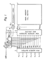
- a 5 which are supplied to row address decoders and drivers 4 for selecting one row memory cell array within the main memory cell matrix 1 and to a decoder 5, which is comprised of a PROM (programmable read-only memory), for selecting the redundancy memory cell array 2 via a driver 8.
- PROM programmable read-only memory
- the decoders and drivers 4, the decoder 5 and the driver 8 are activated by a clock signal WD generated from a clock 6 which, in turn, receives a row address strobe signal RAS.
- the decoders and drivers 4 receive the signal WD through a switching circuit 7.
- the decoder 5 does not perform the selection operation for the redundancy memory cell array 2.
- the device also comprises column address buffers, column address decoders and drivers, sense amplifiers, a data input buffer, a data output buffer or the like which are, however, omitted in Figure 1.
- all memory cells of the main memory cell matrix 1 of a completed semiconductor memory device are tested. After testing, if all of the memory cells of the main memory matrix 1 are determined to be normal, the operation of the device is the same as that of a memory device without the redundancy memory cell array 2, the decoder 5 and the switching circuit 7. In this case, one row array is selected from the main memory cell matrix 1 by the row address decoders and drivers 4 and, after that, one column array is selected from the main memory cell matrix 1 by the column address decoders and drivers (not shown), so that one desired memory cell at an intersecting portion of said one row array and one column is selected. Next, data stored in the desired memory cell is read out to the data output buffer-(not shown), or new data of the data input buffer (not shown) is written into the desired memory cell.
- a row address (hereinafter referred to as a defective row address ADD x ) to which said row memory cell array is written into the decoder 5 by using output signals A o , A o , A 1 , A 1 , ..., A 5 , A 5 of the row address buffers 3.
- the decoding operation for the signals A o , A o , A 1 , A 1 , ..., A 5 , A of the row address buffers 3 is effected by either the row address decoders and drivers 4 or the decoder 5.
- the decoder 5 does not operate, while the row address decoders and drivers 4 operate so as to select one row array among the main memory cell matrix 1.
- the column address decoders and drivers (not shown) operate so as to select one column array of the main memory cell matrix 1. As a result, one normal memory cell of the main memory cell matrix 1 is selected.
- the decoder 5 When the signals A o , A o , A 1 , A 1 , ..., A 5 , A 5 correspond to the defective row address ADD x , the decoder 5 generates a signal RST and activates the driver 8 so as to select the redundancy memory cell array 2 and, accordingly, any of the memory cells of the array 2 can be selected. Simultaneously, the decoder 5 disables the switching circuit 7 by the signal RST so as to stop the transmission of the clock signal WD of the clock 6 to the row address decoders and drivers 4.
- the decoders and drivers 4 cannot execute a selection operation even when the decoders and drivers 4 receive the signals A o , A o , A 1 , A 1 , ..., A 5 , A 5 from the row address buffers 3.
- the column address decoders and drivers (not shown) operate so as to select one memory cell of the redundancy memory cell array 2.
- Figure 2 is a block diagram illustrating another proposed semiconductor memory device including a redundancy memory cell array therein.
- the elements which are the same as those of Figure 1 are denoted by the same reference numerals.
- the switching circuit 7 in Figure 1 is not illustrated and the signal RST of the decoder 5 is supplied directly to the row address decoders and drivers 4'.
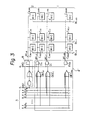
- Figure 3 is a logic circuit diagram of the row address decoders and drivers 4' of Figure 2.
- the row address decoders and drivers 4' comprise decoders DEC o , DEC 1 , ..., DEC 63 formed by NOR gates and word drivers D 0 , D 1 , ..., D 83 formed by AND gates each connected to one of the decoders DEC o , DEC 1 , ..., DEC 63 .
- Each decoder receives the address signals A o (or A o ), A 1 (or A,) ..., A (or A 5 ) from the address buffers 3 ( Figure 2) and the signal RST from the decoder 5 ( Figure 2), while each driver receives the clock signal WD from the clock 6 ( Figure 2).
- the potentials of the signals RST and WD are low and high, respectively, one of word lines WL 0 , WL 1 , ..., WL 63 which corresponds to the address signals A o , A o , A 1 , A 1 , ..., A 5 , A 5 is selected.
- the word lines WL o , WL 1 , ..., WL 63 are connected to the 1 st row memory cell array comprised of memory cells C 00 , C 01 , ..., C o.63 % the 2nd row memory cell array comprised of memory cells C 10 , C 11 , ..., C 1.63 ; and the 64th row memory cell array comprised of memory cells C 63.0' C 63.1 ' ..., C 63.83' res p ec- tively.
- the driver 8 operates so as to select a word line WL R which is connected to the redundancy memory cell array 2 comprised of memory cells C RO' C R1 , ... C R63 '
- FIG 4 is a circuit diagram of the row address decoders and drivers 4' of Figure 2.
- the areas of the transistors Q 41 through Q 48 are relatively small, since each current flowing there through is relatively small.
- each area of the transistors Q 42 is relatively small; however, a large number of the transistors Q 42 , which number is, for example, sixty-four in the case of a 4,096 bit memory device, are necessary so that the entire device becomes large.
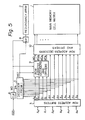
- Figure 5 is a block diagram illustrating an embodiment of the semiconductor memory device according to the present invention.
- the elements which are the same as those of Figure 2 are denoted by the same reference numerals.
- row address decoders and drivers 9 and 10 are provided instead of the row address decoders and drivers 4' of Figure 2.
- the memory cell matrix 1 is divided into a plurality of sub matrix cell matrixes (not shown).
- the row address decoders and drivers 10 is used for selecting one sub memory cell matrix within the main memory cell matrix 1, while the row address decoders and drivers 9 is used for selecting one row memory cell array within each sub memory cell matrix.
- the decoder 5 When the address signals A o , A o , A 1 , A 1 , ..., A 5 , A 5 do not correspond to the defective row address ADD x , the decoder 5 generates the signal RST the potential of which is in this case low, so that the driver 8 is not activated. That is, the redundancy memory cell array 2 is not selected. Simultaneously, the row address decoders and drivers 9 execute a selection operation by using the address signals A o , A o , A 1 and A 1 so as to generate signals WD 1 through WD 4 to the row address decoders and drivers 10. In this case, one of the potentials of the signals WD 1 through WD 4 is high and the others are low.
- the row address decoders and drivers 10 execute a selection operation by using the address signals A 2 , A 2 , ..., A 5 , A 5 and the signals WD 1 through WD 4 , so as to select one row memory cell array within the main memory cell matrix 1.
- the decoder 5 when the address signals A o , A 0 , A,, A 1 , ..., A 5 , A 5 correspond to the defective row address ADD x , the decoder 5 generates the signal RST, the potential of which is, in this case high, so that the driver 8 is activated so as to select the redundancy memory cell array 2.
- the row address decoders and drivers 9 are disabled by the high potential signal RST which also results in disabling of the row address decoders and drivers 10, since all the potentials of the signals WD 1 through WD 4 become low.
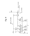
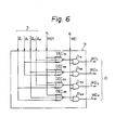
- Figure 6 is a logic circuit diagram of the row address decoders and drivers 9 of Figure 5.
- the row address decoders and drivers 9 comprise decoders DEC 91 through DEC 94 formed by NOR gates and word drivers D 91 through D 94 formed by AND gates.
- Each of the decoders DEC 91 through DEC 94 has an input connected to the output of the decoder 5 ( Figure 5) and inputs for receiving the address signals A o (or A o ) and A 1 (or A 1 ).
- each of the word drivers D 91 through D 94 has an input connected to the clock 6 ( Figure 5) and an input connected to one of the outputs of the decoders DEC 91 through DEC 94 .
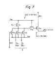
- FIG. 7 is a circuit diagram of the row address decoders and drivers 9 of Figure 5.
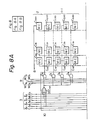
- Figure 8 is a block diagram of the row address decoders and drivers 10 of Figure 5.
- the decoders and drivers 10 comprise decoders DEC 101 through DEC 116 formed by NOR gates which receive the address signals A 2 (or A 2 ), A3 (or A3), A4 (or A4) and A 5 (or A 5 ), and word drivers Do through D 63 .
- the decoder DEC 101 is used for selecting a sub memory cell matrix 1-1 comprised of the memory cells C 00 , C 01 , ..., C 0,63 ; C 10 , C 11 , ..., C 1,63 ; C 20' C 21' ..., C 2,63 ; C 30' C 31' ..., C 3,63'
- the other decoders DEC 102 through DEC 116 are used for selecting sub memory cell matrixes 1-2 through 1-16, respectively.
- the redundancy memory cell array 2 ( Figure 5) is not selected, only one of the potentials of the signals WD 1 through WD 4 is high. For example, the potential of the signal WD 1 is high. As a result, the word drivers Do, D 4 , ..., D 60 are activated. In addition, only one of the potentials of the outputs of the decoders DEC 101 through DEC 108 in accordance with the address signals A 2 , A 2 , ..., A 5 and A 5 is high, for example, the potential of the output of the decoder DEC 101 is high. Therefore, only one row memory cell array formed by the memory cells C 00 , C 01 , .. , C 0,63 is selected.
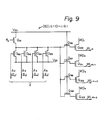
- FIG 9 is a circuit diagram of the row address decoders and drivers 10 of Figure 5.
- the row address decoders and drivers 9 and 10 according to the present invention are simpler than the row address decoders and drivers 4' of the proposed device.
- the number of the transistors Q 72 , the areas of which are small, used for the disabling means is reduced.
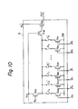
- FIG 10 is a circuit diagram of the decoder 5 of Figure 5.
- the decoder 5 is a PROM of a fuse type which comprises a load transistor Q 105 , transistors Q 106 through Q 117 for receiving the address signals A o , A 0 , A 1 , A 1 , ..., A 5 , A 5 , respectively, and a transistor Q 118 serving as a transfer gate.
- the transistors Q 106 through Q 117 are connected through fuses F 0 ,F 0 ', F 1 , F 1 ', . , Fs, F 5 ' to the transistor Q 105.
- a defective memory cell is detected in the main memory cell matrix 1 ( Figure 1), a row address to which said defective memory cell belongs is written.
- the fuses such as Fo' , F 1 and F s are melted down by a programming means (not shown).
- one redundancy memory cell array 2 is incorporated with the main memory matrix 1 and, accordingly, in spite of a defective memory cell, the device of Figure 5 can be used (in particular cases, two or more defective memory cells are generated in one row array; the device of Figure 5 can thus be used in spite of these defects.).
- two or more redundancy memory cell arrays 2 can be provided. In this case, there can be more than one decoder 5 and more than one redundancy memory cell array 2.
- the redundancy memory cell array 2 is incorporated with the main memory cell matrix 1 along the rows thereof, but the redundancy memory cell array 2 can also be incorporated with the main memory cell matrix 1 along the columns thereof.
- the semiconductor memory device has an advantage, as compared with the proposed device, in that the area of the entire device is reduced, since the decoders and drivers are small.
Landscapes
- Techniques For Improving Reliability Of Storages (AREA)
- For Increasing The Reliability Of Semiconductor Memories (AREA)
- Dram (AREA)
Applications Claiming Priority (2)
| Application Number | Priority Date | Filing Date | Title |
|---|---|---|---|
| JP1979157393U JPS5928560Y2 (ja) | 1979-11-13 | 1979-11-13 | 冗長ビットを有する記憶装置 |
| JP157393/79U | 1979-11-13 |
Publications (2)
| Publication Number | Publication Date |
|---|---|
| EP0029322A1 EP0029322A1 (en) | 1981-05-27 |
| EP0029322B1 true EP0029322B1 (en) | 1984-07-25 |
Family
ID=15648645
Family Applications (1)
| Application Number | Title | Priority Date | Filing Date |
|---|---|---|---|
| EP80303939A Expired EP0029322B1 (en) | 1979-11-13 | 1980-11-05 | Semiconductor memory device with redundancy |
Country Status (4)
| Country | Link |
|---|---|
| US (1) | US4365319A (enExample) |
| EP (1) | EP0029322B1 (enExample) |
| JP (1) | JPS5928560Y2 (enExample) |
| DE (1) | DE3068717D1 (enExample) |
Families Citing this family (37)
| Publication number | Priority date | Publication date | Assignee | Title |
|---|---|---|---|---|
| JPS563499A (en) * | 1979-06-25 | 1981-01-14 | Fujitsu Ltd | Semiconductor memory device |
| US4489402A (en) * | 1981-04-25 | 1984-12-18 | Tokyo Shibaura Denki Kabushiki Kaisha | Semiconductor memory device |
| US4462091A (en) * | 1982-02-26 | 1984-07-24 | International Business Machines Corporation | Word group redundancy scheme |
| JPS58164099A (ja) * | 1982-03-25 | 1983-09-28 | Toshiba Corp | 半導体メモリ− |
| JPS58199496A (ja) * | 1982-05-14 | 1983-11-19 | Hitachi Ltd | 欠陥救済回路を有する半導体メモリ |
| JPS5971199A (ja) * | 1982-10-14 | 1984-04-21 | Toshiba Corp | 半導体メモリ装置 |
| US4494220A (en) * | 1982-11-24 | 1985-01-15 | At&T Bell Laboratories | Folded bit line memory with one decoder per pair of spare rows |
| US4633429A (en) * | 1982-12-27 | 1986-12-30 | Motorola, Inc. | Partial memory selection using a programmable decoder |
| US4556975A (en) * | 1983-02-07 | 1985-12-03 | Westinghouse Electric Corp. | Programmable redundancy circuit |
| JPS59151398A (ja) * | 1983-02-17 | 1984-08-29 | Mitsubishi Electric Corp | 半導体記憶装置 |
| US4577294A (en) * | 1983-04-18 | 1986-03-18 | Advanced Micro Devices, Inc. | Redundant memory circuit and method of programming and verifying the circuit |
| US4590388A (en) * | 1984-04-23 | 1986-05-20 | At&T Bell Laboratories | CMOS spare decoder circuit |
| JPS6143362A (ja) * | 1984-08-07 | 1986-03-01 | Nec Corp | 集積回路装置 |
| JPS6177946A (ja) * | 1984-09-26 | 1986-04-21 | Hitachi Ltd | 半導体記憶装置 |
| US4796233A (en) * | 1984-10-19 | 1989-01-03 | Fujitsu Limited | Bipolar-transistor type semiconductor memory device having redundancy configuration |
| US4744060A (en) * | 1984-10-19 | 1988-05-10 | Fujitsu Limited | Bipolar-transistor type random access memory having redundancy configuration |
| US4740925A (en) * | 1985-10-15 | 1988-04-26 | Texas Instruments Incorporated | Extra row for testing programmability and speed of ROMS |
| JPS62293598A (ja) * | 1986-06-12 | 1987-12-21 | Toshiba Corp | 半導体記憶装置 |
| JPS6337899A (ja) * | 1986-07-30 | 1988-02-18 | Mitsubishi Electric Corp | 半導体記憶装置 |
| EP0257120B1 (de) * | 1986-08-22 | 1992-06-10 | International Business Machines Corporation | Dekodierverfahren und -Schaltungsanordnung für einen redundanten CMOS-Halbleiterspeicher |
| FR2608826B1 (fr) * | 1986-12-19 | 1989-03-17 | Eurotechnique Sa | Circuit integre comportant des elements d'aiguillage vers des elements de redondance dans une memoire |
| US5191224A (en) * | 1987-04-22 | 1993-03-02 | Hitachi, Ltd. | Wafer scale of full wafer memory system, packaging method thereof, and wafer processing method employed therein |
| FR2623653B1 (fr) * | 1987-11-24 | 1992-10-23 | Sgs Thomson Microelectronics | Procede de test de cellules de memoire electriquement programmable et circuit integre correspondant |
| US4885720A (en) * | 1988-04-01 | 1989-12-05 | International Business Machines Corporation | Memory device and method implementing wordline redundancy without an access time penalty |
| US5022006A (en) * | 1988-04-01 | 1991-06-04 | International Business Machines Corporation | Semiconductor memory having bit lines with isolation circuits connected between redundant and normal memory cells |
| US5289417A (en) * | 1989-05-09 | 1994-02-22 | Mitsubishi Denki Kabushiki Kaisha | Semiconductor memory device with redundancy circuit |
| JP2547633B2 (ja) * | 1989-05-09 | 1996-10-23 | 三菱電機株式会社 | 半導体記憶装置 |
| DE69129882T2 (de) * | 1990-06-19 | 1999-03-04 | Texas Instruments Inc., Dallas, Tex. | Assoziatives DRAM-Redundanzschema mit variabler Satzgrösse |
| JP2600018B2 (ja) * | 1990-09-29 | 1997-04-16 | 三菱電機株式会社 | 半導体記憶装置 |
| DE69117926D1 (de) * | 1991-03-29 | 1996-04-18 | Ibm | Speichersystem mit anpassbarer Redundanz |
| JP2738195B2 (ja) * | 1991-12-27 | 1998-04-08 | 日本電気株式会社 | 不揮発性半導体記憶装置 |
| US5557618A (en) * | 1993-01-19 | 1996-09-17 | Tektronix, Inc. | Signal sampling circuit with redundancy |
| EP0657814B1 (en) * | 1993-12-07 | 1999-03-17 | STMicroelectronics S.r.l. | Redundancy circuitry for a semiconductor memory device |
| US5568433A (en) * | 1995-06-19 | 1996-10-22 | International Business Machines Corporation | Memory array having redundant word line |
| EP0798642B1 (en) * | 1996-03-29 | 2001-11-07 | STMicroelectronics S.r.l. | Redundancy management method and architecture, particularly for non-volatile memories |
| WO2004090910A1 (en) * | 2003-04-07 | 2004-10-21 | Koninklijke Philips Electronics N.V. | Semiconductor memory device having redundancy means |
| US10896127B2 (en) | 2013-01-23 | 2021-01-19 | Lucata Corporation | Highly configurable memory architecture for partitioned global address space memory systems |
Family Cites Families (3)
| Publication number | Priority date | Publication date | Assignee | Title |
|---|---|---|---|---|
| US3753244A (en) * | 1971-08-18 | 1973-08-14 | Ibm | Yield enhancement redundancy technique |
| BE789991A (fr) * | 1971-10-12 | 1973-04-12 | Siemens Ag | Dispositif logique, en particulier decodeur a elements redondants |
| US4051354A (en) * | 1975-07-03 | 1977-09-27 | Texas Instruments Incorporated | Fault-tolerant cell addressable array |
-
1979
- 1979-11-13 JP JP1979157393U patent/JPS5928560Y2/ja not_active Expired
-
1980
- 1980-11-05 EP EP80303939A patent/EP0029322B1/en not_active Expired
- 1980-11-05 DE DE8080303939T patent/DE3068717D1/de not_active Expired
- 1980-11-12 US US06/206,272 patent/US4365319A/en not_active Expired - Lifetime
Also Published As
| Publication number | Publication date |
|---|---|
| US4365319A (en) | 1982-12-21 |
| DE3068717D1 (en) | 1984-08-30 |
| JPS5677100U (enExample) | 1981-06-23 |
| JPS5928560Y2 (ja) | 1984-08-17 |
| EP0029322A1 (en) | 1981-05-27 |
Similar Documents
| Publication | Publication Date | Title |
|---|---|---|
| EP0029322B1 (en) | Semiconductor memory device with redundancy | |
| KR950004872B1 (ko) | 정규 메모리 셀 어레이와 동시에 억세스가능한 용장 메모리 셀 컬럼을 갖고 있는 반도체 메모리 디바이스 | |
| US4908798A (en) | Semiconductor memory device with memory cell arrays and a redundant memory cell array associated with a small number of write-in and sense amplifying circuits | |
| EP0031386B1 (en) | Semiconductor memory device | |
| EP0313040B1 (en) | Erasable programmable read only memory device | |
| US4648075A (en) | Redundancy circuit for a semiconductor memory device | |
| JPH0574191A (ja) | 半導体記憶装置 | |
| KR920009059B1 (ko) | 반도체 메모리 장치의 병렬 테스트 방법 | |
| US20010050871A1 (en) | Semiconductor memory integrated circuit | |
| US6307794B1 (en) | Semiconductor memory device and signal line shifting method | |
| US6208569B1 (en) | Method of and apparatus for sharing redundancy circuits between memory arrays within a semiconductor memory device | |
| US6094381A (en) | Semiconductor memory device with redundancy circuit | |
| US6122207A (en) | Semiconductor memory device and method for relieving defective memory cells | |
| EP0686980B1 (en) | Semiconductor memory device having means for replacing defective memory cells | |
| US5218572A (en) | Semiconductor memory device | |
| US5359563A (en) | Memory system with adaptable redundancy | |
| US4584674A (en) | Semiconductor memory device with improved memory arrangement | |
| JP2596180B2 (ja) | 半導体集積メモリ回路 | |
| EP0329182A2 (en) | Decoder buffer circuit incorporated in semiconductor memory device | |
| US6249466B1 (en) | Row redundancy scheme | |
| US6320814B1 (en) | Semiconductor device | |
| JP2695411B2 (ja) | 半導体記憶装置 | |
| JP2009123258A (ja) | 半導体記憶装置 | |
| JPS58137191A (ja) | 半導体メモリ | |
| JPH06259987A (ja) | 半導体記憶装置 |
Legal Events
| Date | Code | Title | Description |
|---|---|---|---|
| PUAI | Public reference made under article 153(3) epc to a published international application that has entered the european phase |
Free format text: ORIGINAL CODE: 0009012 |
|
| 17P | Request for examination filed |
Effective date: 19801110 |
|
| AK | Designated contracting states |
Designated state(s): DE FR GB NL |
|
| GRAA | (expected) grant |
Free format text: ORIGINAL CODE: 0009210 |
|
| PGFP | Annual fee paid to national office [announced via postgrant information from national office to epo] |
Ref country code: FR Payment date: 19840702 Year of fee payment: 5 |
|
| AK | Designated contracting states |
Designated state(s): DE FR GB NL |
|
| REF | Corresponds to: |
Ref document number: 3068717 Country of ref document: DE Date of ref document: 19840830 |
|
| ET | Fr: translation filed | ||
| PLBI | Opposition filed |
Free format text: ORIGINAL CODE: 0009260 |
|
| PLBI | Opposition filed |
Free format text: ORIGINAL CODE: 0009260 |
|
| 26 | Opposition filed |
Opponent name: SIEMENS AKTIENGESELLSCHAFT, BERLIN UND MUENCHEN Effective date: 19850423 |
|
| 26 | Opposition filed |
Opponent name: TELEFUNKEN ELECTRONIC GMBH Effective date: 19850425 |
|
| NLR1 | Nl: opposition has been filed with the epo |
Opponent name: SIEMENS AKTIENGESELLSCHAFT |
|
| NLR1 | Nl: opposition has been filed with the epo |
Opponent name: TELEFUNKEN ELECTRONIC GMBH |
|
| PGFP | Annual fee paid to national office [announced via postgrant information from national office to epo] |
Ref country code: NL Payment date: 19871130 Year of fee payment: 8 |
|
| PGFP | Annual fee paid to national office [announced via postgrant information from national office to epo] |
Ref country code: DE Payment date: 19890126 Year of fee payment: 9 |
|
| RDAG | Patent revoked |
Free format text: ORIGINAL CODE: 0009271 |
|
| STAA | Information on the status of an ep patent application or granted ep patent |
Free format text: STATUS: PATENT REVOKED |
|
| 27W | Patent revoked |
Effective date: 19890713 |
|
| GBPR | Gb: patent revoked under art. 102 of the ep convention designating the uk as contracting state | ||
| NLR2 | Nl: decision of opposition | ||
| APAH | Appeal reference modified |
Free format text: ORIGINAL CODE: EPIDOSCREFNO |