EP0010633A1 - Procédé pour former des zones de dopage très étroites dans un corps semiconducteur et utilisation de ce procédé pour produire des zones semiconductrices isolées l'une contre l'autre, des dispositifs bipolaires à semiconducteurs, circuits intégrés logiques à injection et des transistors à effet de champ et à double diffusion - Google Patents
Procédé pour former des zones de dopage très étroites dans un corps semiconducteur et utilisation de ce procédé pour produire des zones semiconductrices isolées l'une contre l'autre, des dispositifs bipolaires à semiconducteurs, circuits intégrés logiques à injection et des transistors à effet de champ et à double diffusion Download PDFInfo
- Publication number
- EP0010633A1 EP0010633A1 EP79103770A EP79103770A EP0010633A1 EP 0010633 A1 EP0010633 A1 EP 0010633A1 EP 79103770 A EP79103770 A EP 79103770A EP 79103770 A EP79103770 A EP 79103770A EP 0010633 A1 EP0010633 A1 EP 0010633A1
- Authority
- EP
- European Patent Office
- Prior art keywords
- regions
- layer
- semiconductor
- doping
- narrow
- Prior art date
- Legal status (The legal status is an assumption and is not a legal conclusion. Google has not performed a legal analysis and makes no representation as to the accuracy of the status listed.)
- Granted
Links
- 238000000034 method Methods 0.000 title claims abstract description 61
- 239000004065 semiconductor Substances 0.000 title claims abstract description 36
- 238000004519 manufacturing process Methods 0.000 title claims abstract description 6
- 238000002347 injection Methods 0.000 title claims description 5
- 239000007924 injection Substances 0.000 title claims description 5
- 238000001020 plasma etching Methods 0.000 claims abstract description 18
- 238000009792 diffusion process Methods 0.000 claims abstract description 14
- 239000002019 doping agent Substances 0.000 claims abstract description 11
- 230000008961 swelling Effects 0.000 claims abstract description 9
- 230000015572 biosynthetic process Effects 0.000 claims abstract description 8
- 238000010438 heat treatment Methods 0.000 claims abstract description 6
- VYPSYNLAJGMNEJ-UHFFFAOYSA-N Silicium dioxide Chemical compound O=[Si]=O VYPSYNLAJGMNEJ-UHFFFAOYSA-N 0.000 claims description 36
- 230000008569 process Effects 0.000 claims description 28
- 229910021420 polycrystalline silicon Inorganic materials 0.000 claims description 20
- 235000012239 silicon dioxide Nutrition 0.000 claims description 18
- 239000000377 silicon dioxide Substances 0.000 claims description 18
- 238000002955 isolation Methods 0.000 claims description 6
- 239000000463 material Substances 0.000 claims description 5
- 239000013078 crystal Substances 0.000 claims description 2
- 239000010410 layer Substances 0.000 claims 17
- 230000001590 oxidative effect Effects 0.000 claims 1
- 230000035515 penetration Effects 0.000 claims 1
- 239000000126 substance Substances 0.000 claims 1
- 239000002344 surface layer Substances 0.000 claims 1
- 238000005530 etching Methods 0.000 abstract description 17
- 238000001459 lithography Methods 0.000 abstract description 8
- 238000010276 construction Methods 0.000 abstract description 3
- 230000008901 benefit Effects 0.000 abstract description 2
- 238000007493 shaping process Methods 0.000 abstract description 2
- XUIMIQQOPSSXEZ-UHFFFAOYSA-N Silicon Chemical compound [Si] XUIMIQQOPSSXEZ-UHFFFAOYSA-N 0.000 description 14
- 229910052710 silicon Inorganic materials 0.000 description 14
- 239000010703 silicon Substances 0.000 description 14
- 239000000758 substrate Substances 0.000 description 10
- 238000005516 engineering process Methods 0.000 description 9
- 230000000873 masking effect Effects 0.000 description 6
- QVGXLLKOCUKJST-UHFFFAOYSA-N atomic oxygen Chemical compound [O] QVGXLLKOCUKJST-UHFFFAOYSA-N 0.000 description 5
- 238000009388 chemical precipitation Methods 0.000 description 5
- 229910021419 crystalline silicon Inorganic materials 0.000 description 5
- 239000007789 gas Substances 0.000 description 5
- 239000011810 insulating material Substances 0.000 description 5
- 230000003647 oxidation Effects 0.000 description 5
- 238000007254 oxidation reaction Methods 0.000 description 5
- 239000001301 oxygen Substances 0.000 description 5
- 229910052760 oxygen Inorganic materials 0.000 description 5
- 101100390736 Danio rerio fign gene Proteins 0.000 description 4
- 101100390738 Mus musculus Fign gene Proteins 0.000 description 4
- 238000009413 insulation Methods 0.000 description 4
- 238000005468 ion implantation Methods 0.000 description 4
- 229910052698 phosphorus Inorganic materials 0.000 description 4
- 229910052581 Si3N4 Inorganic materials 0.000 description 3
- 150000002500 ions Chemical class 0.000 description 3
- 229910052751 metal Inorganic materials 0.000 description 3
- 239000002184 metal Substances 0.000 description 3
- 238000012856 packing Methods 0.000 description 3
- 238000000206 photolithography Methods 0.000 description 3
- HQVNEWCFYHHQES-UHFFFAOYSA-N silicon nitride Chemical compound N12[Si]34N5[Si]62N3[Si]51N64 HQVNEWCFYHHQES-UHFFFAOYSA-N 0.000 description 3
- OAICVXFJPJFONN-UHFFFAOYSA-N Phosphorus Chemical compound [P] OAICVXFJPJFONN-UHFFFAOYSA-N 0.000 description 2
- BLRPTPMANUNPDV-UHFFFAOYSA-N Silane Chemical compound [SiH4] BLRPTPMANUNPDV-UHFFFAOYSA-N 0.000 description 2
- 238000001015 X-ray lithography Methods 0.000 description 2
- 229910052782 aluminium Inorganic materials 0.000 description 2
- XAGFODPZIPBFFR-UHFFFAOYSA-N aluminium Chemical compound [Al] XAGFODPZIPBFFR-UHFFFAOYSA-N 0.000 description 2
- 229910052785 arsenic Inorganic materials 0.000 description 2
- RQNWIZPPADIBDY-UHFFFAOYSA-N arsenic atom Chemical compound [As] RQNWIZPPADIBDY-UHFFFAOYSA-N 0.000 description 2
- 239000000460 chlorine Substances 0.000 description 2
- 239000003989 dielectric material Substances 0.000 description 2
- 150000002739 metals Chemical class 0.000 description 2
- 239000000203 mixture Substances 0.000 description 2
- 229910052757 nitrogen Inorganic materials 0.000 description 2
- 230000003287 optical effect Effects 0.000 description 2
- 239000011574 phosphorus Substances 0.000 description 2
- 239000007787 solid Substances 0.000 description 2
- 239000000243 solution Substances 0.000 description 2
- XLYOFNOQVPJJNP-UHFFFAOYSA-N water Chemical compound O XLYOFNOQVPJJNP-UHFFFAOYSA-N 0.000 description 2
- ZCYVEMRRCGMTRW-UHFFFAOYSA-N 7553-56-2 Chemical compound [I] ZCYVEMRRCGMTRW-UHFFFAOYSA-N 0.000 description 1
- ZOXJGFHDIHLPTG-UHFFFAOYSA-N Boron Chemical compound [B] ZOXJGFHDIHLPTG-UHFFFAOYSA-N 0.000 description 1
- WKBOTKDWSSQWDR-UHFFFAOYSA-N Bromine atom Chemical compound [Br] WKBOTKDWSSQWDR-UHFFFAOYSA-N 0.000 description 1
- ZAMOUSCENKQFHK-UHFFFAOYSA-N Chlorine atom Chemical compound [Cl] ZAMOUSCENKQFHK-UHFFFAOYSA-N 0.000 description 1
- UFHFLCQGNIYNRP-UHFFFAOYSA-N Hydrogen Chemical compound [H][H] UFHFLCQGNIYNRP-UHFFFAOYSA-N 0.000 description 1
- 229910003902 SiCl 4 Inorganic materials 0.000 description 1
- WPPDFTBPZNZZRP-UHFFFAOYSA-N aluminum copper Chemical compound [Al].[Cu] WPPDFTBPZNZZRP-UHFFFAOYSA-N 0.000 description 1
- 229910052787 antimony Inorganic materials 0.000 description 1
- WATWJIUSRGPENY-UHFFFAOYSA-N antimony atom Chemical compound [Sb] WATWJIUSRGPENY-UHFFFAOYSA-N 0.000 description 1
- 239000003963 antioxidant agent Substances 0.000 description 1
- 230000003078 antioxidant effect Effects 0.000 description 1
- 229910052796 boron Inorganic materials 0.000 description 1
- GDTBXPJZTBHREO-UHFFFAOYSA-N bromine Substances BrBr GDTBXPJZTBHREO-UHFFFAOYSA-N 0.000 description 1
- 229910052794 bromium Inorganic materials 0.000 description 1
- 230000008859 change Effects 0.000 description 1
- 238000005234 chemical deposition Methods 0.000 description 1
- 229910052801 chlorine Inorganic materials 0.000 description 1
- 239000000470 constituent Substances 0.000 description 1
- 238000007796 conventional method Methods 0.000 description 1
- 238000005520 cutting process Methods 0.000 description 1
- 230000007547 defect Effects 0.000 description 1
- 238000011161 development Methods 0.000 description 1
- 238000000609 electron-beam lithography Methods 0.000 description 1
- 230000005669 field effect Effects 0.000 description 1
- 239000003574 free electron Substances 0.000 description 1
- 239000011521 glass Substances 0.000 description 1
- 239000001257 hydrogen Substances 0.000 description 1
- 229910052739 hydrogen Inorganic materials 0.000 description 1
- 230000010354 integration Effects 0.000 description 1
- 239000011630 iodine Substances 0.000 description 1
- 229910052740 iodine Inorganic materials 0.000 description 1
- 229910021421 monocrystalline silicon Inorganic materials 0.000 description 1
- TWNQGVIAIRXVLR-UHFFFAOYSA-N oxo(oxoalumanyloxy)alumane Chemical compound O=[Al]O[Al]=O TWNQGVIAIRXVLR-UHFFFAOYSA-N 0.000 description 1
- 229920002120 photoresistant polymer Polymers 0.000 description 1
- 229910021426 porous silicon Inorganic materials 0.000 description 1
- 238000012545 processing Methods 0.000 description 1
- 230000005855 radiation Effects 0.000 description 1
- 230000009257 reactivity Effects 0.000 description 1
- 230000009467 reduction Effects 0.000 description 1
- 238000000926 separation method Methods 0.000 description 1
- 229910000077 silane Inorganic materials 0.000 description 1
- 238000000992 sputter etching Methods 0.000 description 1
- 238000007740 vapor deposition Methods 0.000 description 1
Images


Classifications
-
- H—ELECTRICITY
- H01—ELECTRIC ELEMENTS
- H01L—SEMICONDUCTOR DEVICES NOT COVERED BY CLASS H10
- H01L29/00—Semiconductor devices specially adapted for rectifying, amplifying, oscillating or switching and having potential barriers; Capacitors or resistors having potential barriers, e.g. a PN-junction depletion layer or carrier concentration layer; Details of semiconductor bodies or of electrodes thereof ; Multistep manufacturing processes therefor
- H01L29/66—Types of semiconductor device ; Multistep manufacturing processes therefor
- H01L29/66007—Multistep manufacturing processes
- H01L29/66075—Multistep manufacturing processes of devices having semiconductor bodies comprising group 14 or group 13/15 materials
- H01L29/66227—Multistep manufacturing processes of devices having semiconductor bodies comprising group 14 or group 13/15 materials the devices being controllable only by the electric current supplied or the electric potential applied, to an electrode which does not carry the current to be rectified, amplified or switched, e.g. three-terminal devices
- H01L29/66409—Unipolar field-effect transistors
- H01L29/66477—Unipolar field-effect transistors with an insulated gate, i.e. MISFET
- H01L29/66545—Unipolar field-effect transistors with an insulated gate, i.e. MISFET using a dummy, i.e. replacement gate in a process wherein at least a part of the final gate is self aligned to the dummy gate
-
- H—ELECTRICITY
- H01—ELECTRIC ELEMENTS
- H01L—SEMICONDUCTOR DEVICES NOT COVERED BY CLASS H10
- H01L21/00—Processes or apparatus adapted for the manufacture or treatment of semiconductor or solid state devices or of parts thereof
- H01L21/02—Manufacture or treatment of semiconductor devices or of parts thereof
- H01L21/027—Making masks on semiconductor bodies for further photolithographic processing not provided for in group H01L21/18 or H01L21/34
- H01L21/033—Making masks on semiconductor bodies for further photolithographic processing not provided for in group H01L21/18 or H01L21/34 comprising inorganic layers
- H01L21/0334—Making masks on semiconductor bodies for further photolithographic processing not provided for in group H01L21/18 or H01L21/34 comprising inorganic layers characterised by their size, orientation, disposition, behaviour, shape, in horizontal or vertical plane
- H01L21/0337—Making masks on semiconductor bodies for further photolithographic processing not provided for in group H01L21/18 or H01L21/34 comprising inorganic layers characterised by their size, orientation, disposition, behaviour, shape, in horizontal or vertical plane characterised by the process involved to create the mask, e.g. lift-off masks, sidewalls, or to modify the mask, e.g. pre-treatment, post-treatment
-
- H—ELECTRICITY
- H01—ELECTRIC ELEMENTS
- H01L—SEMICONDUCTOR DEVICES NOT COVERED BY CLASS H10
- H01L21/00—Processes or apparatus adapted for the manufacture or treatment of semiconductor or solid state devices or of parts thereof
- H01L21/02—Manufacture or treatment of semiconductor devices or of parts thereof
- H01L21/04—Manufacture or treatment of semiconductor devices or of parts thereof the devices having potential barriers, e.g. a PN junction, depletion layer or carrier concentration layer
- H01L21/18—Manufacture or treatment of semiconductor devices or of parts thereof the devices having potential barriers, e.g. a PN junction, depletion layer or carrier concentration layer the devices having semiconductor bodies comprising elements of Group IV of the Periodic Table or AIIIBV compounds with or without impurities, e.g. doping materials
- H01L21/22—Diffusion of impurity materials, e.g. doping materials, electrode materials, into or out of a semiconductor body, or between semiconductor regions; Interactions between two or more impurities; Redistribution of impurities
- H01L21/225—Diffusion of impurity materials, e.g. doping materials, electrode materials, into or out of a semiconductor body, or between semiconductor regions; Interactions between two or more impurities; Redistribution of impurities using diffusion into or out of a solid from or into a solid phase, e.g. a doped oxide layer
- H01L21/2251—Diffusion into or out of group IV semiconductors
- H01L21/2254—Diffusion into or out of group IV semiconductors from or through or into an applied layer, e.g. photoresist, nitrides
- H01L21/2255—Diffusion into or out of group IV semiconductors from or through or into an applied layer, e.g. photoresist, nitrides the applied layer comprising oxides only, e.g. P2O5, PSG, H3BO3, doped oxides
-
- H—ELECTRICITY
- H01—ELECTRIC ELEMENTS
- H01L—SEMICONDUCTOR DEVICES NOT COVERED BY CLASS H10
- H01L21/00—Processes or apparatus adapted for the manufacture or treatment of semiconductor or solid state devices or of parts thereof
- H01L21/02—Manufacture or treatment of semiconductor devices or of parts thereof
- H01L21/04—Manufacture or treatment of semiconductor devices or of parts thereof the devices having potential barriers, e.g. a PN junction, depletion layer or carrier concentration layer
- H01L21/18—Manufacture or treatment of semiconductor devices or of parts thereof the devices having potential barriers, e.g. a PN junction, depletion layer or carrier concentration layer the devices having semiconductor bodies comprising elements of Group IV of the Periodic Table or AIIIBV compounds with or without impurities, e.g. doping materials
- H01L21/22—Diffusion of impurity materials, e.g. doping materials, electrode materials, into or out of a semiconductor body, or between semiconductor regions; Interactions between two or more impurities; Redistribution of impurities
- H01L21/225—Diffusion of impurity materials, e.g. doping materials, electrode materials, into or out of a semiconductor body, or between semiconductor regions; Interactions between two or more impurities; Redistribution of impurities using diffusion into or out of a solid from or into a solid phase, e.g. a doped oxide layer
- H01L21/2251—Diffusion into or out of group IV semiconductors
- H01L21/2254—Diffusion into or out of group IV semiconductors from or through or into an applied layer, e.g. photoresist, nitrides
- H01L21/2257—Diffusion into or out of group IV semiconductors from or through or into an applied layer, e.g. photoresist, nitrides the applied layer being silicon or silicide or SIPOS, e.g. polysilicon, porous silicon
-
- H—ELECTRICITY
- H01—ELECTRIC ELEMENTS
- H01L—SEMICONDUCTOR DEVICES NOT COVERED BY CLASS H10
- H01L29/00—Semiconductor devices specially adapted for rectifying, amplifying, oscillating or switching and having potential barriers; Capacitors or resistors having potential barriers, e.g. a PN-junction depletion layer or carrier concentration layer; Details of semiconductor bodies or of electrodes thereof ; Multistep manufacturing processes therefor
- H01L29/66—Types of semiconductor device ; Multistep manufacturing processes therefor
- H01L29/66007—Multistep manufacturing processes
- H01L29/66075—Multistep manufacturing processes of devices having semiconductor bodies comprising group 14 or group 13/15 materials
- H01L29/66227—Multistep manufacturing processes of devices having semiconductor bodies comprising group 14 or group 13/15 materials the devices being controllable only by the electric current supplied or the electric potential applied, to an electrode which does not carry the current to be rectified, amplified or switched, e.g. three-terminal devices
- H01L29/66234—Bipolar junction transistors [BJT]
- H01L29/66272—Silicon vertical transistors
-
- H—ELECTRICITY
- H01—ELECTRIC ELEMENTS
- H01L—SEMICONDUCTOR DEVICES NOT COVERED BY CLASS H10
- H01L29/00—Semiconductor devices specially adapted for rectifying, amplifying, oscillating or switching and having potential barriers; Capacitors or resistors having potential barriers, e.g. a PN-junction depletion layer or carrier concentration layer; Details of semiconductor bodies or of electrodes thereof ; Multistep manufacturing processes therefor
- H01L29/66—Types of semiconductor device ; Multistep manufacturing processes therefor
- H01L29/68—Types of semiconductor device ; Multistep manufacturing processes therefor controllable by only the electric current supplied, or only the electric potential applied, to an electrode which does not carry the current to be rectified, amplified or switched
- H01L29/76—Unipolar devices, e.g. field effect transistors
- H01L29/772—Field effect transistors
- H01L29/78—Field effect transistors with field effect produced by an insulated gate
- H01L29/7833—Field effect transistors with field effect produced by an insulated gate with lightly doped drain or source extension, e.g. LDD MOSFET's; DDD MOSFET's
-
- Y—GENERAL TAGGING OF NEW TECHNOLOGICAL DEVELOPMENTS; GENERAL TAGGING OF CROSS-SECTIONAL TECHNOLOGIES SPANNING OVER SEVERAL SECTIONS OF THE IPC; TECHNICAL SUBJECTS COVERED BY FORMER USPC CROSS-REFERENCE ART COLLECTIONS [XRACs] AND DIGESTS
- Y10—TECHNICAL SUBJECTS COVERED BY FORMER USPC
- Y10S—TECHNICAL SUBJECTS COVERED BY FORMER USPC CROSS-REFERENCE ART COLLECTIONS [XRACs] AND DIGESTS
- Y10S148/00—Metal treatment
- Y10S148/131—Reactive ion etching rie
Definitions
- the invention relates to methods for producing very narrow doping regions in a semiconductor body using a diffusion of the respective dopants from associated source layer regions.
- reactive ion etching can be used to carry out anisotropic etching with the high so-called aspect ratio Ratios can be achieved, ie the etching rate in the vertical direction is considerably more pronounced than that in the horizontal direction.
- a plasma or ionized gas is required for carrying out the process, for which a large number of highly reactive constituents, e.g. B. ions, free electrons and free radicals are decisive.
- the plasma used for the etching can be kept at relatively low temperatures in the order of up to approximately 250 ° C.
- the plasma components are mainly free radicals, which cause the intense reactivity of the plasma.
- the ion occupancy in a low temperature plasma is on the order of about 1% of the components.
- the polycrystalline silicon layer can later either be removed or left as part of the respective component.
- reference can be made, for example, to US Pat. Nos. 3,978,515, 3,502,517 and the article "Polycrystalline Silicon as a Diffusion Source and Interconnect Layer in I 2 L Realizations", by Jan Middelhoek and others, published in the IEEE Journal of Solid-State Circuits, Vol. SC-12, No. 2, April 1977, pages 135 to 138.
- the invention solves the problem of expanding the area of application of conventionally designed lithography processes to further reduced dimensions down to the submicron range in order to produce doping regions of extremely small dimensions for the construction of highly integrated circuits.
- a surface which has essentially horizontal and vertical surface areas is first formed by applying and shaping insulating layer areas on a semiconductor body.
- a source layer doped in the desired type of doping is then applied to the surface obtained in this way.
- the swelling layer is removed from the horizontal surface areas.
- only very narrow swelling layer areas remain on the vertically oriented surfaces.
- the formation of the ultimately very narrow doping regions is finally carried out by a heat treatment known per se from the very narrow source layer regions. Their width can be varied with the selected layer thickness of the swelling layer.
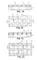
- 1A shows a small section of a silicon body in high magnification, in which the respective integrated circuit is to be produced with a high packing density.
- a single crystal e.g. B. P-type silicon substrate 10
- the layer labeled 12 can be composed of a variety of materials or combinations thereof, including silicon dioxide, silicon nitride, aluminum oxide and the like. This first insulating layer 12 is partially removed in the manner shown in FIG.
- a reactive ion etching method of the type described in more detail in the literature mentioned at the beginning can preferably be used.
- the respective process atmosphere depends on the material of the insulating layer to be treated, cf. insofar the article "A Survey of Plasma-Etching Processes" by Richard L. Bersin, also given at the beginning.
- a second layer 14 is then applied to the surface.
- This second layer can consist of an insulating material, polycrystalline silicon or the like and is highly doped with a P + dopant, e.g. B. in this example with boron.
- the second layer is applied to the surface as a result of the aforementioned etching process of the first insulating layer 12, which has essentially horizontal and essentially vertical surface areas.
- FIG. 1A shows a top view of FIG. 1A, the section line for the cross section according to FIG. 1A also being indicated.
- the P + dopants are introduced into the P substrate 10 from the narrow, vertically aligned layer regions 14 by means of thermal diffusion.
- the layers labeled 12 and 14 can then preferably be removed for further processing.
- the result after said diffusion is shown in FIG. 1C, the doping regions being able to serve, for example, as channel stoppers for MOS-FET circuits.
- the diffusion pattern generated in this way can also be used for the isolation by means of blocked semiconductor junctions between bipolar structures, which can subsequently be built up in the areas thus delimited in a manner known per se.
- FIG. 1D again shows a plan view of the semiconductor arrangement produced so far, the cutting line for the cross section shown in FIG. 1C being also indicated. It can be seen that the isolation pattern is a checkerboard pattern; Of course, other insulation patterns can also be produced using the method mentioned.
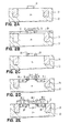
- FIG. 2A again shows a small section of a single-crystalline silicon body in high magnification, in which Such a double-diffused FET circuit is to be introduced with a high packing density.
- the starting point is a P-type substrate 22 with a crystallographic ⁇ 100> orientation and a specific resistance value in the order of 1 to 20 2 'cm.
- Zones designated 24 are provided for the isolation of single-crystalline regions in the substrate 22. These can be partial or complete dielectric isolation zones, silicon dioxide, silicon nitride, glass, etc. being usable as dielectric materials.
- partial dielectric insulation of the form shown in FIG. 2A is preferably used. There are many ways to form these isolation areas, cf. preferably the method described in detail in the aforementioned US Pat. No. 4,104,086.
- a silicon dioxide layer 26 of approximately 500 nm thickness is subsequently applied by means of thermal oxidation or by chemical deposition from the gas phase.
- An oxygen or oxygen / water vapor atmosphere at about 970 ° C. is used for the thermal growth.
- a process atmosphere made of SiH 4 , O 2 , at about 450 ° C or SiH 2 Cl 2 , N 2 0 at about 800 ° C and atmospheric pressure or lower is used.
- the silicon dioxide layer other insulating layers or combinations thereof can also be provided.
- Openings are made in the first insulating layer 26 using standard photolithography and etching processes. Alternatively, reactive ion etching can also be used. The openings in layer 26 are opened at the locations provided for the source and drain of the double-diffused FET structures.
- a second layer 28 is then applied to the essentially horizontal surface areas 30 and vertical surface areas 32.
- this layer 28 consists of chemically deposited silicon dioxide in accordance with the previously described method or of polycrystalline silicon.
- the layer designated 28 is heavily P + doped.
- a suitable layer thickness of the silicon dioxide is between about 50 and 2000 nm, preferably at 400 nm. If the layer is thicker than 2000 nm, charge transport problems and longer etching times occur. With a layer thickness ⁇ 100 nm, there is a risk of short circuits.
- the structure shown in FIG. 2B is then introduced into a suitable process atmosphere for reactive ion etching of the material of the layer designated by 28. Essentially the horizontal areas of the layer 28 are removed, so that the very small-sized vertical area areas according to FIG. 2C remain.
- N + ions are diffused in through the source and drain openings.
- either a thermal diffusion process or an ion implantation with phosphorus, arsenic or antimony or the like can be used as the N dopant.
- P + dopants diffuse from the (remaining) layer regions 28 into the substrate 22, so that the very narrow P channel region 34 is defined in this way.
- the N + doping region 36 preferably extends deeper into the substrate than such a P doping region 34.
- the resulting structure is shown in FIG. 2D.
- the preferred physical dimensions of the structure are for a P region 34 a width of approximately 500 nm at a depth of approximately 200 nm and for such a region total N + region 36 a depth of about 300 nm.
- the layers labeled 26 and 28 can first be removed. Then a silicon dioxide layer denoted by 37 is grown on g , for which purpose a low-temperature process is preferably used, e.g. B. a chemical precipitation from the gas phase of the type described above or a thermal oxidation process. It was found that in a dry oxygen atmosphere at 800 or 900 ° C., the oxide growth takes place more quickly in an area heavily doped with phosphorus and results in a much thicker oxide layer than in a slightly N or P doped area. Such a method is described, for example, in the article "Thermal Oxidation of Heavily Phosphorus-Doped Silicon" by CP Ho et al., Published in J.
- the gate electrode 38 and the source and drain connections 39 and 40 are formed by first applying a continuous conductive layer, e.g. B. made of aluminum, and subsequently etched in a manner known per se.
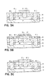
- 3A again shows a small section of the silicon body in question, in which such a bipolar circuit is to be formed.
- NPN transistors can be produced in this embodiment PNP transistors can be produced in the same way with a corresponding change in the choice of conductivity types.
- a continuous N + doping for a sub-collector 43 is provided in a P-substrate 42 made of single-crystal silicon.
- An N-epitaxial layer 44 is located thereon.
- the process steps concerned in this regard are process steps customary in bipolar technology.
- the substrate has a crystallographic ⁇ 100> orientation and a specific resistance value on the order of 1 to 20 ⁇ ⁇ cm.
- the subcollector diffusion is carried out using arsenic with a surface concentration of approximately 10 20 / cm 3 over 10 0 min. at 1200 ° C.
- the step for producing the epitaxial layer 44 can be carried out conventionally, e.g. B. using SiCl 4 / H 2 or SiH4 / H2 mixtures at temperatures of 1000 to 1200 ° C.
- the dopants contained in the N + layer migrate into the epitaxial layer.
- the thickness of the epitaxial layer has values of about ⁇ 3 ⁇ m for highly integrated circuits.
- a mask (not shown) is applied, in which mask windows are opened by suitable photolithography and etching processes at the locations provided for the dielectric insulation of the single-crystalline silicon regions and the base / emitter and collector connection regions.
- the insulation regions denoted by 46 in FIG. 3A separate the single-crystalline silicon regions from one another; 47 denotes a separation region which separates a base / emitter region from a collector connection region.
- 47 denotes a separation region which separates a base / emitter region from a collector connection region.
- a P-conductive base region 45 is then created by ion implantation or thermal diffusion with a surface concentration of approximately 5 ⁇ 10 19 / cm 3 over 40 minutes at approximately 925 ° C.
- All silicon dioxide is then removed from the surface of the device.
- An insulating layer 50 e.g. B. from thermally grown silicon dioxide, is then applied to the surface of the semiconductor body, the dielectric regions 46 and 47 also extending to this surface.
- This insulating layer can again consist of any suitable insulating material of the type mentioned in the other exemplary embodiments. Using standard lithography and etching processes, 50 windows are opened in this layer at the locations provided for the emitter and collector connection areas. Reactive ion etching can also be used for this.
- the insulating layer 50 etched in this way has essentially horizontal and essentially vertical surface areas.
- a polycrystalline silicon layer is preferred. It is applied by means of chemical precipitation from the gas phase, for example a mixture of silane and a conduction type-changing (P or N) dopant is used in a hydrogen-containing atmosphere at a temperature in the range of 500 to 1000 ° C.
- the polycrystalline silicon can first be applied (undoped) and only then doped by means of ion implantation.
- the thickness of the second insulating layer is expediently between approximately 100 and 1000 nm, preferably 400 nm.
- this layer determines the size of the emitter area and the width of the collector connection regions.
- 3B is then introduced into a reactive etching atmosphere for polycrystalline silicon.
- 3C is removed from all horizontal surface areas in accordance with FIG. 3C.
- a silicon dioxide layer is thermally grown at about 970 ° C in an oxygen or oxygen / water vapor atmosphere on the silicon surface to form the layer labeled 54.
- the structure shown in FIG. 3D is exposed to a temperature in the range from approximately 1000 to 1100 ° C. for approximately 100 to 300 minutes in order to move the N + dopants from the vertically oriented regions of the layer 52 to form the emitter 56 into the P base region 45 or to form the collector connection area 58 into the associated N area.
- a so-called block-out or rough masking 60 is then applied from a suitable photoresist, exposed and developed in order to produce an opening in the silicon dioxide layer 54 to the base region 45.
- the layer labeled 60 is then removed again.
- the silicon dioxide layer 54 is removed down to the polycrystalline silicon layer 52 and this layer 52 is partially or even removed down to the silicon regions 56 and 58.
- emitter, base and collector connections 61, 62 and 64 are formed by using conventional methods Ren a conductive layer is applied and shape etched in the desired pattern.
- the base contact hole and the contact holes for the emitter and collector connection area can also be formed with a single masking step, if necessary.
- FIGS. 4A to 4D The last exemplary embodiment shown in FIGS. 4A to 4D is intended to deal with the application of the invention for producing an integrated injection logic circuit in bipolar technology.
- 4A again shows a small section of a silicon body, in which the circuit is to be formed, in high magnification.
- the semiconductor arrangement shown in FIG. 4A is manufactured in a similar manner to that described for FIG. 3A, with largely the same reference numerals being used.
- two P regions 70 and 72 are now provided in at least some of the dielectrically isolated single-crystalline silicon regions.
- An insulating layer 74 is applied to the semiconductor body by means of thermal oxidation or by chemical precipitation. This layer can consist of one or a combination of different insulating materials of the types mentioned above.
- Openings are formed in the layer using standard lithography and etching methods, including reactive ion etching.
- the layer 74 remains in the manner indicated in FIG. 4A over a partial area of one of the P areas. This results in a surface with horizontal and vertical surface areas 75 and 76 with respect to the layer and the substrate.
- a layer of polycrystalline silicon is preferred. This polycrystalline silicon layer is again formed by means of chemical precipitation from the gas phase according to the example based on FIGS. 3A to 3F described previous embodiment.
- the semiconductor arrangement processed so far is then introduced into a process atmosphere for reactive ion etching of the polycrystalline silicon.
- the layer denoted by 74 is removed essentially from all horizontal surface areas, but is left on the vertical surface areas according to FIG. 4B.
- a layer of silicon dioxide, labeled 80, is then grown on the silicon surface in the manner previously described.
- the structure shown in FIG. 4C is heated to about 1000 to 1100 ° C. for 100 to 300 minutes in order to allow the N + dopants to penetrate into the P region 72 from the remaining regions of the layer 78 to form the N regions 81 and 82.
- the connections of the integrated injection logic circuit produced in this way are made in a manner known per se by forming a rough masking and etching the polycrystalline silicon with subsequent metal vapor deposition in the manner described above with reference to FIGS. 3A to 3F.
- the electrode 84 contacts the area 70, the electrode 85 the area 81 and the electrode 86 the area 82.
- the areas designated 44 and 72 are also provided with electrodes for the completion of the circuit, but this is no longer shown in FIG. 4D , because it can be conventional measures. Further details of this type of circuit can also be found in US Pat. No. 3,736,477.
Landscapes
- Engineering & Computer Science (AREA)
- Microelectronics & Electronic Packaging (AREA)
- Power Engineering (AREA)
- General Physics & Mathematics (AREA)
- Computer Hardware Design (AREA)
- Physics & Mathematics (AREA)
- Condensed Matter Physics & Semiconductors (AREA)
- Manufacturing & Machinery (AREA)
- Ceramic Engineering (AREA)
- Chemical & Material Sciences (AREA)
- Inorganic Chemistry (AREA)
- Bipolar Transistors (AREA)
- Drying Of Semiconductors (AREA)
Applications Claiming Priority (2)
| Application Number | Priority Date | Filing Date | Title |
|---|---|---|---|
| US05/957,599 US4209350A (en) | 1978-11-03 | 1978-11-03 | Method for forming diffusions having narrow dimensions utilizing reactive ion etching |
| US957599 | 1978-11-03 |
Publications (2)
| Publication Number | Publication Date |
|---|---|
| EP0010633A1 true EP0010633A1 (fr) | 1980-05-14 |
| EP0010633B1 EP0010633B1 (fr) | 1982-10-13 |
Family
ID=25499826
Family Applications (1)
| Application Number | Title | Priority Date | Filing Date |
|---|---|---|---|
| EP79103770A Expired EP0010633B1 (fr) | 1978-11-03 | 1979-10-03 | Procédé pour former des zones de dopage très étroites dans un corps semiconducteur et utilisation de ce procédé pour produire des zones semiconductrices isolées l'une contre l'autre, des dispositifs bipolaires à semiconducteurs, circuits intégrés logiques à injection et des transistors à effet de champ et à double diffusion |
Country Status (6)
| Country | Link |
|---|---|
| US (1) | US4209350A (fr) |
| EP (1) | EP0010633B1 (fr) |
| JP (2) | JPS5562725A (fr) |
| CA (1) | CA1120610A (fr) |
| DE (1) | DE2963852D1 (fr) |
| IT (1) | IT1164518B (fr) |
Cited By (8)
| Publication number | Priority date | Publication date | Assignee | Title |
|---|---|---|---|---|
| EP0083785A2 (fr) * | 1981-12-30 | 1983-07-20 | International Business Machines Corporation | Procédé pour la fabrication de transistors à effet de champ auto-alignés pour circuits intégrés |
| EP0113405A2 (fr) * | 1982-12-13 | 1984-07-18 | International Business Machines Corporation | Procédé pour la fabrication d'une résistance à semi-conducteur |
| WO1986003620A2 (fr) * | 1984-12-10 | 1986-06-19 | Ncr Corporation | Procede de formation de regions de diffusion dans un substrat semiconducteur |
| WO1987002825A1 (fr) * | 1985-11-02 | 1987-05-07 | Plessey Overseas Limited | Procede de fabrication de transistors mos |
| EP0258147A2 (fr) * | 1986-08-28 | 1988-03-02 | Fairchild Semiconductor Corporation | Procédé pour fabriquer un transistor du type bipolaire comportant un ruban en polysilicium |
| EP0450503A2 (fr) * | 1990-04-02 | 1991-10-09 | National Semiconductor Corporation | Dispositifs semi-conducteurs ayant des parois latérales d'espacement en verre borosilicaté et leur procédé de fabrication |
| EP0484321A1 (fr) * | 1987-08-24 | 1992-05-06 | Hitachi, Ltd. | Méthode de fabrication d'un dispositif semi-conducteur à porte isolée |
| US5179034A (en) * | 1987-08-24 | 1993-01-12 | Hitachi, Ltd. | Method for fabricating insulated gate semiconductor device |
Families Citing this family (57)
| Publication number | Priority date | Publication date | Assignee | Title |
|---|---|---|---|---|
| US4274909A (en) * | 1980-03-17 | 1981-06-23 | International Business Machines Corporation | Method for forming ultra fine deep dielectric isolation |
| US4319932A (en) * | 1980-03-24 | 1982-03-16 | International Business Machines Corporation | Method of making high performance bipolar transistor with polysilicon base contacts |
| US5202574A (en) * | 1980-05-02 | 1993-04-13 | Texas Instruments Incorporated | Semiconductor having improved interlevel conductor insulation |
| US4359816A (en) * | 1980-07-08 | 1982-11-23 | International Business Machines Corporation | Self-aligned metal process for field effect transistor integrated circuits |
| US4513303A (en) * | 1980-07-08 | 1985-04-23 | International Business Machines Corporation | Self-aligned metal field effect transistor integrated circuit |
| US4400865A (en) * | 1980-07-08 | 1983-08-30 | International Business Machines Corporation | Self-aligned metal process for integrated circuit metallization |
| US4758528A (en) * | 1980-07-08 | 1988-07-19 | International Business Machines Corporation | Self-aligned metal process for integrated circuit metallization |
| US4488162A (en) * | 1980-07-08 | 1984-12-11 | International Business Machines Corporation | Self-aligned metal field effect transistor integrated circuits using polycrystalline silicon gate electrodes |
| US4358340A (en) * | 1980-07-14 | 1982-11-09 | Texas Instruments Incorporated | Submicron patterning without using submicron lithographic technique |
| US4394196A (en) * | 1980-07-16 | 1983-07-19 | Tokyo Shibaura Denki Kabushiki Kaisha | Method of etching, refilling and etching dielectric grooves for isolating micron size device regions |
| JPS5758356A (en) * | 1980-09-26 | 1982-04-08 | Toshiba Corp | Manufacture of semiconductor device |
| US4366613A (en) * | 1980-12-17 | 1983-01-04 | Ibm Corporation | Method of fabricating an MOS dynamic RAM with lightly doped drain |
| NL188432C (nl) * | 1980-12-26 | 1992-06-16 | Nippon Telegraph & Telephone | Werkwijze voor het vervaardigen van een mosfet. |
| US4438556A (en) * | 1981-01-12 | 1984-03-27 | Tokyo Shibaura Denki Kabushiki Kaisha | Method of forming doped polycrystalline silicon pattern by selective implantation and plasma etching of undoped regions |
| US4414737A (en) * | 1981-01-30 | 1983-11-15 | Tokyo Shibaura Denki Kabushiki Kaisha | Production of Schottky barrier diode |
| US4691435A (en) * | 1981-05-13 | 1987-09-08 | International Business Machines Corporation | Method for making Schottky diode having limited area self-aligned guard ring |
| JPS581878A (ja) * | 1981-06-26 | 1983-01-07 | Fujitsu Ltd | 磁気バブルメモリ素子の製造方法 |
| JPS5848936A (ja) * | 1981-09-10 | 1983-03-23 | Fujitsu Ltd | 半導体装置の製造方法 |
| US4430791A (en) * | 1981-12-30 | 1984-02-14 | International Business Machines Corporation | Sub-micrometer channel length field effect transistor process |
| US4419809A (en) * | 1981-12-30 | 1983-12-13 | International Business Machines Corporation | Fabrication process of sub-micrometer channel length MOSFETs |
| US4445267A (en) * | 1981-12-30 | 1984-05-01 | International Business Machines Corporation | MOSFET Structure and process to form micrometer long source/drain spacing |
| NL8105920A (nl) * | 1981-12-31 | 1983-07-18 | Philips Nv | Halfgeleiderinrichting en werkwijze voor het vervaardigen van een dergelijke halfgeleiderinrichting. |
| JPS58151390A (ja) * | 1982-02-16 | 1983-09-08 | ザ・ベンデイツクス・コ−ポレ−シヨン | 非結晶質基板上に単結晶膜を形成する方法 |
| US4712125A (en) * | 1982-08-06 | 1987-12-08 | International Business Machines Corporation | Structure for contacting a narrow width PN junction region |
| US4507171A (en) * | 1982-08-06 | 1985-03-26 | International Business Machines Corporation | Method for contacting a narrow width PN junction region |
| JPS59138379A (ja) * | 1983-01-27 | 1984-08-08 | Toshiba Corp | 半導体装置の製造方法 |
| US4641170A (en) * | 1983-12-12 | 1987-02-03 | International Business Machines Corporation | Self-aligned lateral bipolar transistors |
| US4551906A (en) * | 1983-12-12 | 1985-11-12 | International Business Machines Corporation | Method for making self-aligned lateral bipolar transistors |
| US4546535A (en) * | 1983-12-12 | 1985-10-15 | International Business Machines Corporation | Method of making submicron FET structure |
| US4636834A (en) * | 1983-12-12 | 1987-01-13 | International Business Machines Corporation | Submicron FET structure and method of making |
| US4671830A (en) * | 1984-01-03 | 1987-06-09 | Xerox Corporation | Method of controlling the modeling of the well energy band profile by interdiffusion |
| US4599789A (en) * | 1984-06-15 | 1986-07-15 | Harris Corporation | Process of making twin well VLSI CMOS |
| US4574469A (en) * | 1984-09-14 | 1986-03-11 | Motorola, Inc. | Process for self-aligned buried layer, channel-stop, and isolation |
| US4649638A (en) * | 1985-04-17 | 1987-03-17 | International Business Machines Corp. | Construction of short-length electrode in semiconductor device |
| US4714686A (en) * | 1985-07-31 | 1987-12-22 | Advanced Micro Devices, Inc. | Method of forming contact plugs for planarized integrated circuits |
| US4843023A (en) * | 1985-09-25 | 1989-06-27 | Hewlett-Packard Company | Process for forming lightly-doped-drain (LDD) without extra masking steps |
| JPS62277745A (ja) * | 1986-05-27 | 1987-12-02 | Toshiba Corp | 半導体集積回路 |
| US5063168A (en) * | 1986-07-02 | 1991-11-05 | National Semiconductor Corporation | Process for making bipolar transistor with polysilicon stringer base contact |
| JPH0650741B2 (ja) * | 1986-12-26 | 1994-06-29 | 富士通株式会社 | 半導体装置とその製造方法 |
| US4933295A (en) * | 1987-05-08 | 1990-06-12 | Raytheon Company | Method of forming a bipolar transistor having closely spaced device regions |
| EP0313683A1 (fr) * | 1987-10-30 | 1989-05-03 | International Business Machines Corporation | Méthode pour fabriquer une structure de circuit intégré semi-conducteur comprenant un élément de longueur submicrométrique |
| US4818714A (en) * | 1987-12-02 | 1989-04-04 | Advanced Micro Devices, Inc. | Method of making a high performance MOS device having LDD regions with graded junctions |
| EP0338102B1 (fr) * | 1988-04-19 | 1993-03-10 | International Business Machines Corporation | Procédé de fabrication de circuits intégrés à semi-conducteurs comportant des transistors à effet de champ ayant des canaux submicroniques |
| US5015595A (en) * | 1988-09-09 | 1991-05-14 | Advanced Micro Devices, Inc. | Method of making a high performance MOS device having both P- and N-LDD regions using single photoresist mask |
| US5064773A (en) * | 1988-12-27 | 1991-11-12 | Raytheon Company | Method of forming bipolar transistor having closely spaced device regions |
| US5026663A (en) * | 1989-07-21 | 1991-06-25 | Motorola, Inc. | Method of fabricating a structure having self-aligned diffused junctions |
| US5116778A (en) * | 1990-02-05 | 1992-05-26 | Advanced Micro Devices, Inc. | Dopant sources for cmos device |
| US5071780A (en) * | 1990-08-27 | 1991-12-10 | Taiwan Semiconductor Manufacturing Company, Ltd. | Reverse self-aligned transistor integrated circuit |
| US5235204A (en) * | 1990-08-27 | 1993-08-10 | Taiwan Semiconductor Manufacturing Company | Reverse self-aligned transistor integrated circuit |
| US5175606A (en) * | 1990-08-27 | 1992-12-29 | Taiwan Semiconductor Manufacturing Company | Reverse self-aligned BiMOS transistor integrated circuit |
| US5028557A (en) * | 1990-08-27 | 1991-07-02 | Taiwan Semiconductor Manufacturing Co., Ltd. | Method of making a reverse self-aligned BIMOS transistor integrated circuit |
| US5466615A (en) * | 1993-08-19 | 1995-11-14 | Taiwan Semiconductor Manufacturing Company Ltd. | Silicon damage free process for double poly emitter and reverse MOS in BiCMOS application |
| US5518945A (en) * | 1995-05-05 | 1996-05-21 | International Business Machines Corporation | Method of making a diffused lightly doped drain device with built in etch stop |
| EP0853815A4 (fr) * | 1995-10-04 | 1999-10-27 | Intel Corp | Formation d'une region de source et de drain en verre dope |
| US6306702B1 (en) | 1999-08-24 | 2001-10-23 | Advanced Micro Devices, Inc. | Dual spacer method of forming CMOS transistors with substantially the same sub 0.25 micron gate length |
| US6372589B1 (en) * | 2000-04-19 | 2002-04-16 | Advanced Micro Devices, Inc. | Method of forming ultra-shallow source/drain extension by impurity diffusion from doped dielectric spacer |
| DE10330838B4 (de) | 2003-07-08 | 2005-08-25 | Infineon Technologies Ag | Elektronisches Bauelement mit Schutzring |
Citations (1)
| Publication number | Priority date | Publication date | Assignee | Title |
|---|---|---|---|---|
| DE2818090A1 (de) * | 1977-04-25 | 1978-11-02 | Nippon Telegraph & Telephone | Bipolartransistor und verfahren zur herstellung desselben |
Family Cites Families (11)
| Publication number | Priority date | Publication date | Assignee | Title |
|---|---|---|---|---|
| DE1464921B2 (de) * | 1963-10-03 | 1971-10-07 | Fujitsu Ltd , Kawasaki, Kanagawa (Japan) | Verfahren zum herstellen einer halbleiteranordnung |
| US3730787A (en) * | 1970-08-26 | 1973-05-01 | Bell Telephone Labor Inc | Method of fabricating semiconductor integrated circuits using deposited doped oxides as a source of dopant impurities |
| US3966577A (en) * | 1973-08-27 | 1976-06-29 | Trw Inc. | Dielectrically isolated semiconductor devices |
| US4124933A (en) * | 1974-05-21 | 1978-11-14 | U.S. Philips Corporation | Methods of manufacturing semiconductor devices |
| US4037307A (en) * | 1975-03-21 | 1977-07-26 | Bell Telephone Laboratories, Incorporated | Methods for making transistor structures |
| US4026740A (en) * | 1975-10-29 | 1977-05-31 | Intel Corporation | Process for fabricating narrow polycrystalline silicon members |
| US4103415A (en) * | 1976-12-09 | 1978-08-01 | Fairchild Camera And Instrument Corporation | Insulated-gate field-effect transistor with self-aligned contact hole to source or drain |
| US4139442A (en) * | 1977-09-13 | 1979-02-13 | International Business Machines Corporation | Reactive ion etching method for producing deep dielectric isolation in silicon |
| JPS5444483A (en) * | 1977-09-14 | 1979-04-07 | Matsushita Electric Ind Co Ltd | Mos type semiconductor device and its manufacture |
| US4160991A (en) * | 1977-10-25 | 1979-07-10 | International Business Machines Corporation | High performance bipolar device and method for making same |
| US4157269A (en) * | 1978-06-06 | 1979-06-05 | International Business Machines Corporation | Utilizing polysilicon diffusion sources and special masking techniques |
-
1978
- 1978-11-03 US US05/957,599 patent/US4209350A/en not_active Expired - Lifetime
-
1979
- 1979-10-03 CA CA000336936A patent/CA1120610A/fr not_active Expired
- 1979-10-03 DE DE7979103770T patent/DE2963852D1/de not_active Expired
- 1979-10-03 EP EP79103770A patent/EP0010633B1/fr not_active Expired
- 1979-10-12 JP JP13093979A patent/JPS5562725A/ja active Granted
- 1979-10-26 IT IT26808/79A patent/IT1164518B/it active
-
1985
- 1985-08-20 JP JP60181182A patent/JPS61159768A/ja active Granted
Patent Citations (1)
| Publication number | Priority date | Publication date | Assignee | Title |
|---|---|---|---|---|
| DE2818090A1 (de) * | 1977-04-25 | 1978-11-02 | Nippon Telegraph & Telephone | Bipolartransistor und verfahren zur herstellung desselben |
Non-Patent Citations (2)
| Title |
|---|
| IBM TECHNICAL DISCLOSURE BULLETIN, Band 21, Heft 9, Februar 1979 New York J.L. DEINES et al. "Process for realization of submicron geometries" Seiten 3628 bis 3629 * Seite 3629; Fig. 2 und 3 * * |
| SOLID STATE TECHNOLOGY, Band 19, Heft 4, April 1976 Port Washington PER G. GLOERSEN "Masking for ion beam etching" * Seiten 68 bis 73 * * |
Cited By (16)
| Publication number | Priority date | Publication date | Assignee | Title |
|---|---|---|---|---|
| EP0083785A2 (fr) * | 1981-12-30 | 1983-07-20 | International Business Machines Corporation | Procédé pour la fabrication de transistors à effet de champ auto-alignés pour circuits intégrés |
| EP0083785A3 (en) * | 1981-12-30 | 1985-01-23 | International Business Machines Corporation | Method of forming self-aligned field effect transistors in integrated circuit structures |
| EP0113405A2 (fr) * | 1982-12-13 | 1984-07-18 | International Business Machines Corporation | Procédé pour la fabrication d'une résistance à semi-conducteur |
| EP0113405A3 (en) * | 1982-12-13 | 1986-07-23 | International Business Machines Corporation | Method for making semiconductor resistors |
| WO1986003620A2 (fr) * | 1984-12-10 | 1986-06-19 | Ncr Corporation | Procede de formation de regions de diffusion dans un substrat semiconducteur |
| WO1986003620A3 (fr) * | 1984-12-10 | 1986-07-31 | Ncr Co | Procede de formation de regions de diffusion dans un substrat semiconducteur |
| WO1987002825A1 (fr) * | 1985-11-02 | 1987-05-07 | Plessey Overseas Limited | Procede de fabrication de transistors mos |
| US4837179A (en) * | 1985-11-02 | 1989-06-06 | Plessey Overseas Limited | Method of making a LDD mosfet |
| EP0258147A3 (fr) * | 1986-08-28 | 1988-08-10 | Fairchild Semiconductor Corporation | Procédé pour fabriquer un transistor du type bipolaire comportant un ruban en polysilicium |
| EP0258147A2 (fr) * | 1986-08-28 | 1988-03-02 | Fairchild Semiconductor Corporation | Procédé pour fabriquer un transistor du type bipolaire comportant un ruban en polysilicium |
| EP0484321A1 (fr) * | 1987-08-24 | 1992-05-06 | Hitachi, Ltd. | Méthode de fabrication d'un dispositif semi-conducteur à porte isolée |
| US5179034A (en) * | 1987-08-24 | 1993-01-12 | Hitachi, Ltd. | Method for fabricating insulated gate semiconductor device |
| EP0604392A1 (fr) * | 1987-08-24 | 1994-06-29 | Hitachi, Ltd. | Dispositif semi-conducteur à porte isolée |
| EP0450503A2 (fr) * | 1990-04-02 | 1991-10-09 | National Semiconductor Corporation | Dispositifs semi-conducteurs ayant des parois latérales d'espacement en verre borosilicaté et leur procédé de fabrication |
| EP0450503A3 (en) * | 1990-04-02 | 1992-05-20 | National Semiconductor Corporation | Semiconductor devices with borosilicate glass sidewall spacers and method of fabrication |
| US5443994A (en) * | 1990-04-02 | 1995-08-22 | National Semiconductor Corporation | Method of fabricating a semiconductor device having a borosilicate glass spacer |
Also Published As
| Publication number | Publication date |
|---|---|
| US4209350A (en) | 1980-06-24 |
| IT7926808A0 (it) | 1979-10-26 |
| JPH0347577B2 (fr) | 1991-07-19 |
| JPS5562725A (en) | 1980-05-12 |
| IT1164518B (it) | 1987-04-15 |
| CA1120610A (fr) | 1982-03-23 |
| EP0010633B1 (fr) | 1982-10-13 |
| JPS61159768A (ja) | 1986-07-19 |
| JPS6250969B2 (fr) | 1987-10-28 |
| DE2963852D1 (en) | 1982-11-18 |
Similar Documents
| Publication | Publication Date | Title |
|---|---|---|
| EP0010633B1 (fr) | Procédé pour former des zones de dopage très étroites dans un corps semiconducteur et utilisation de ce procédé pour produire des zones semiconductrices isolées l'une contre l'autre, des dispositifs bipolaires à semiconducteurs, circuits intégrés logiques à injection et des transistors à effet de champ et à double diffusion | |
| EP0010624B1 (fr) | Procédé pour la réalisation d'ouvertures de masque très petites pour la fabrication de circuits intégrés à semiconducteurs | |
| EP0010596B1 (fr) | Méthode de formation d'ouvertures dans des masques pour la production de circuits semiconducteurs | |
| EP0010623B1 (fr) | Procédé pour la fabrication d'une structure laminée pour des dispositifs à semi-conducteur hautement intégrés avec une couche isolante entre deux couches conductrices | |
| EP0001550B1 (fr) | Dispositif semiconducteur à intégration avec de petites structures et procédé pour sa fabrication | |
| DE69133316T2 (de) | Verfahren zum Herstellen einer Halbleitervorrichtung | |
| EP0000897B1 (fr) | Procédé de fabrication de régions de silicium isolées latéralement | |
| EP0111086B1 (fr) | Procédé pour la fabrication de structures à dimensions sub-micrométriques et application de ce procédé pour la fabrication de régions d'isolation diélectrique profondes à largeur sub-micrométrique dans un corps semi-conducteur | |
| DE2745857C2 (fr) | ||
| DE3841588C2 (fr) | ||
| DE2317577C2 (de) | Verfahren zur Herstellung dielektrisch isolierter Halbleiteranordnungen | |
| DE2502235C2 (fr) | ||
| EP0001574B1 (fr) | Dispositif semiconducteur pour structures de résistance dans des circuits intégrés de haute densité et procédé pour sa fabrication | |
| DE19806838A1 (de) | Vertikaler Siliciumcarbid-MOSFET und Verfahren zur Herstellung desselben | |
| DE2744059A1 (de) | Verfahren zur gemeinsamen integrierten herstellung von feldeffekt- und bipolar-transistoren | |
| DE19909993A1 (de) | Verfahren zum Bilden von Bipolartransistoren mit selbstausrichtender epitaktischer Basis | |
| DE102011088584B4 (de) | Halbleiterbauelement und Verfahren zu seiner Herstellung | |
| DE2626739A1 (de) | Verfahren zur herstellung von monolithisch integrierten halbleiterschaltungen mit durch ionenbombardement hervorgerufenen dielektrischen isolationszonen | |
| DE2445879C2 (de) | Verfahren zum Herstellen eines Halbleiterbauelementes | |
| DE2749607C3 (de) | Halbleiteranordnung und Verfahren zu deren Herstellung | |
| EP0981155A2 (fr) | Procédé de fabrication d'une couche isolante en semi-conducteur et dispositif semi-conducteur contenant cette couche isolante en semi-conducteur | |
| DE19853268C2 (de) | Feldeffektgesteuerter Transistor und Verfahren zu dessen Herstellung | |
| DE3940674C2 (fr) | ||
| DE2449012A1 (de) | Verfahren zur herstellung von dielektrisch isolierten halbleiterbereichen | |
| DE2729973A1 (de) | Verfahren zur herstellung einer halbleiteranordnung |
Legal Events
| Date | Code | Title | Description |
|---|---|---|---|
| PUAI | Public reference made under article 153(3) epc to a published international application that has entered the european phase |
Free format text: ORIGINAL CODE: 0009012 |
|
| AK | Designated contracting states |
Designated state(s): DE FR GB |
|
| 17P | Request for examination filed |
Effective date: 19801007 |
|
| GRAA | (expected) grant |
Free format text: ORIGINAL CODE: 0009210 |
|
| AK | Designated contracting states |
Designated state(s): DE FR GB |
|
| REF | Corresponds to: |
Ref document number: 2963852 Country of ref document: DE Date of ref document: 19821118 |
|
| ITF | It: translation for a ep patent filed |
Owner name: SAIC BREVETTI S.R.L. |
|
| PGFP | Annual fee paid to national office [announced via postgrant information from national office to epo] |
Ref country code: FR Payment date: 19900926 Year of fee payment: 12 |
|
| PG25 | Lapsed in a contracting state [announced via postgrant information from national office to epo] |
Ref country code: FR Effective date: 19920630 |
|
| REG | Reference to a national code |
Ref country code: FR Ref legal event code: ST |
|
| PGFP | Annual fee paid to national office [announced via postgrant information from national office to epo] |
Ref country code: GB Payment date: 19981001 Year of fee payment: 20 |
|
| PGFP | Annual fee paid to national office [announced via postgrant information from national office to epo] |
Ref country code: DE Payment date: 19981019 Year of fee payment: 20 |
|
| PG25 | Lapsed in a contracting state [announced via postgrant information from national office to epo] |
Ref country code: GB Free format text: LAPSE BECAUSE OF EXPIRATION OF PROTECTION Effective date: 19991002 |
|
| REG | Reference to a national code |
Ref country code: GB Ref legal event code: PE20 Effective date: 19991002 |
|
| PLBE | No opposition filed within time limit |
Free format text: ORIGINAL CODE: 0009261 |
|
| STAA | Information on the status of an ep patent application or granted ep patent |
Free format text: STATUS: NO OPPOSITION FILED WITHIN TIME LIMIT |