CN1248552C - Printed circuit board with improved pad structure - Google Patents
Printed circuit board with improved pad structure Download PDFInfo
- Publication number
- CN1248552C CN1248552C CNB021222908A CN02122290A CN1248552C CN 1248552 C CN1248552 C CN 1248552C CN B021222908 A CNB021222908 A CN B021222908A CN 02122290 A CN02122290 A CN 02122290A CN 1248552 C CN1248552 C CN 1248552C
- Authority
- CN
- China
- Prior art keywords
- circuit board
- printed circuit
- pcb
- pads
- pad
- Prior art date
- Legal status (The legal status is an assumption and is not a legal conclusion. Google has not performed a legal analysis and makes no representation as to the accuracy of the status listed.)
- Expired - Fee Related
Links
- 239000004065 semiconductor Substances 0.000 claims abstract description 19
- 239000000758 substrate Substances 0.000 claims description 14
- 238000005538 encapsulation Methods 0.000 claims description 12
- 238000003466 welding Methods 0.000 claims description 5
- 230000002093 peripheral effect Effects 0.000 abstract description 9
- 229910000679 solder Inorganic materials 0.000 abstract description 3
- 230000010354 integration Effects 0.000 abstract 1
- 238000005476 soldering Methods 0.000 abstract 1
- 230000007797 corrosion Effects 0.000 description 2
- 238000005260 corrosion Methods 0.000 description 2
- 239000003822 epoxy resin Substances 0.000 description 2
- 230000003647 oxidation Effects 0.000 description 2
- 238000007254 oxidation reaction Methods 0.000 description 2
- 229920000647 polyepoxide Polymers 0.000 description 2
- 229920005989 resin Polymers 0.000 description 2
- 239000011347 resin Substances 0.000 description 2
- 239000000919 ceramic Substances 0.000 description 1
- 238000010586 diagram Methods 0.000 description 1
- 230000009977 dual effect Effects 0.000 description 1
- 238000009434 installation Methods 0.000 description 1
- 238000004806 packaging method and process Methods 0.000 description 1
- 239000004033 plastic Substances 0.000 description 1
- 238000005728 strengthening Methods 0.000 description 1
Images


Classifications
-
- H—ELECTRICITY
- H05—ELECTRIC TECHNIQUES NOT OTHERWISE PROVIDED FOR
- H05K—PRINTED CIRCUITS; CASINGS OR CONSTRUCTIONAL DETAILS OF ELECTRIC APPARATUS; MANUFACTURE OF ASSEMBLAGES OF ELECTRICAL COMPONENTS
- H05K3/00—Apparatus or processes for manufacturing printed circuits
- H05K3/30—Assembling printed circuits with electric components, e.g. with resistor
- H05K3/32—Assembling printed circuits with electric components, e.g. with resistor electrically connecting electric components or wires to printed circuits
- H05K3/34—Assembling printed circuits with electric components, e.g. with resistor electrically connecting electric components or wires to printed circuits by soldering
- H05K3/341—Surface mounted components
- H05K3/3431—Leadless components
- H05K3/3436—Leadless components having an array of bottom contacts, e.g. pad grid array or ball grid array components
-
- H—ELECTRICITY
- H01—ELECTRIC ELEMENTS
- H01L—SEMICONDUCTOR DEVICES NOT COVERED BY CLASS H10
- H01L23/00—Details of semiconductor or other solid state devices
- H01L23/48—Arrangements for conducting electric current to or from the solid state body in operation, e.g. leads, terminal arrangements ; Selection of materials therefor
- H01L23/488—Arrangements for conducting electric current to or from the solid state body in operation, e.g. leads, terminal arrangements ; Selection of materials therefor consisting of soldered or bonded constructions
- H01L23/498—Leads, i.e. metallisations or lead-frames on insulating substrates, e.g. chip carriers
- H01L23/49838—Geometry or layout
-
- H—ELECTRICITY
- H05—ELECTRIC TECHNIQUES NOT OTHERWISE PROVIDED FOR
- H05K—PRINTED CIRCUITS; CASINGS OR CONSTRUCTIONAL DETAILS OF ELECTRIC APPARATUS; MANUFACTURE OF ASSEMBLAGES OF ELECTRICAL COMPONENTS
- H05K1/00—Printed circuits
- H05K1/02—Details
- H05K1/11—Printed elements for providing electric connections to or between printed circuits
- H05K1/111—Pads for surface mounting, e.g. lay-out
-
- H—ELECTRICITY
- H01—ELECTRIC ELEMENTS
- H01L—SEMICONDUCTOR DEVICES NOT COVERED BY CLASS H10
- H01L2224/00—Indexing scheme for arrangements for connecting or disconnecting semiconductor or solid-state bodies and methods related thereto as covered by H01L24/00
- H01L2224/01—Means for bonding being attached to, or being formed on, the surface to be connected, e.g. chip-to-package, die-attach, "first-level" interconnects; Manufacturing methods related thereto
- H01L2224/02—Bonding areas; Manufacturing methods related thereto
- H01L2224/04—Structure, shape, material or disposition of the bonding areas prior to the connecting process
- H01L2224/05—Structure, shape, material or disposition of the bonding areas prior to the connecting process of an individual bonding area
- H01L2224/0554—External layer
- H01L2224/05599—Material
-
- H—ELECTRICITY
- H01—ELECTRIC ELEMENTS
- H01L—SEMICONDUCTOR DEVICES NOT COVERED BY CLASS H10
- H01L2224/00—Indexing scheme for arrangements for connecting or disconnecting semiconductor or solid-state bodies and methods related thereto as covered by H01L24/00
- H01L2224/01—Means for bonding being attached to, or being formed on, the surface to be connected, e.g. chip-to-package, die-attach, "first-level" interconnects; Manufacturing methods related thereto
- H01L2224/42—Wire connectors; Manufacturing methods related thereto
- H01L2224/44—Structure, shape, material or disposition of the wire connectors prior to the connecting process
- H01L2224/45—Structure, shape, material or disposition of the wire connectors prior to the connecting process of an individual wire connector
- H01L2224/45001—Core members of the connector
- H01L2224/45099—Material
-
- H—ELECTRICITY
- H01—ELECTRIC ELEMENTS
- H01L—SEMICONDUCTOR DEVICES NOT COVERED BY CLASS H10
- H01L2224/00—Indexing scheme for arrangements for connecting or disconnecting semiconductor or solid-state bodies and methods related thereto as covered by H01L24/00
- H01L2224/01—Means for bonding being attached to, or being formed on, the surface to be connected, e.g. chip-to-package, die-attach, "first-level" interconnects; Manufacturing methods related thereto
- H01L2224/42—Wire connectors; Manufacturing methods related thereto
- H01L2224/47—Structure, shape, material or disposition of the wire connectors after the connecting process
- H01L2224/48—Structure, shape, material or disposition of the wire connectors after the connecting process of an individual wire connector
- H01L2224/481—Disposition
- H01L2224/48151—Connecting between a semiconductor or solid-state body and an item not being a semiconductor or solid-state body, e.g. chip-to-substrate, chip-to-passive
- H01L2224/48221—Connecting between a semiconductor or solid-state body and an item not being a semiconductor or solid-state body, e.g. chip-to-substrate, chip-to-passive the body and the item being stacked
- H01L2224/48225—Connecting between a semiconductor or solid-state body and an item not being a semiconductor or solid-state body, e.g. chip-to-substrate, chip-to-passive the body and the item being stacked the item being non-metallic, e.g. insulating substrate with or without metallisation
- H01L2224/48227—Connecting between a semiconductor or solid-state body and an item not being a semiconductor or solid-state body, e.g. chip-to-substrate, chip-to-passive the body and the item being stacked the item being non-metallic, e.g. insulating substrate with or without metallisation connecting the wire to a bond pad of the item
-
- H—ELECTRICITY
- H01—ELECTRIC ELEMENTS
- H01L—SEMICONDUCTOR DEVICES NOT COVERED BY CLASS H10
- H01L2224/00—Indexing scheme for arrangements for connecting or disconnecting semiconductor or solid-state bodies and methods related thereto as covered by H01L24/00
- H01L2224/73—Means for bonding being of different types provided for in two or more of groups H01L2224/10, H01L2224/18, H01L2224/26, H01L2224/34, H01L2224/42, H01L2224/50, H01L2224/63, H01L2224/71
- H01L2224/732—Location after the connecting process
- H01L2224/73251—Location after the connecting process on different surfaces
- H01L2224/73265—Layer and wire connectors
-
- H—ELECTRICITY
- H01—ELECTRIC ELEMENTS
- H01L—SEMICONDUCTOR DEVICES NOT COVERED BY CLASS H10
- H01L2224/00—Indexing scheme for arrangements for connecting or disconnecting semiconductor or solid-state bodies and methods related thereto as covered by H01L24/00
- H01L2224/80—Methods for connecting semiconductor or other solid state bodies using means for bonding being attached to, or being formed on, the surface to be connected
- H01L2224/85—Methods for connecting semiconductor or other solid state bodies using means for bonding being attached to, or being formed on, the surface to be connected using a wire connector
- H01L2224/8538—Bonding interfaces outside the semiconductor or solid-state body
- H01L2224/85399—Material
-
- H—ELECTRICITY
- H01—ELECTRIC ELEMENTS
- H01L—SEMICONDUCTOR DEVICES NOT COVERED BY CLASS H10
- H01L24/00—Arrangements for connecting or disconnecting semiconductor or solid-state bodies; Methods or apparatus related thereto
- H01L24/01—Means for bonding being attached to, or being formed on, the surface to be connected, e.g. chip-to-package, die-attach, "first-level" interconnects; Manufacturing methods related thereto
- H01L24/42—Wire connectors; Manufacturing methods related thereto
- H01L24/47—Structure, shape, material or disposition of the wire connectors after the connecting process
- H01L24/48—Structure, shape, material or disposition of the wire connectors after the connecting process of an individual wire connector
-
- H—ELECTRICITY
- H01—ELECTRIC ELEMENTS
- H01L—SEMICONDUCTOR DEVICES NOT COVERED BY CLASS H10
- H01L2924/00—Indexing scheme for arrangements or methods for connecting or disconnecting semiconductor or solid-state bodies as covered by H01L24/00
- H01L2924/0001—Technical content checked by a classifier
- H01L2924/00014—Technical content checked by a classifier the subject-matter covered by the group, the symbol of which is combined with the symbol of this group, being disclosed without further technical details
-
- H—ELECTRICITY
- H01—ELECTRIC ELEMENTS
- H01L—SEMICONDUCTOR DEVICES NOT COVERED BY CLASS H10
- H01L2924/00—Indexing scheme for arrangements or methods for connecting or disconnecting semiconductor or solid-state bodies as covered by H01L24/00
- H01L2924/15—Details of package parts other than the semiconductor or other solid state devices to be connected
- H01L2924/151—Die mounting substrate
- H01L2924/153—Connection portion
- H01L2924/1531—Connection portion the connection portion being formed only on the surface of the substrate opposite to the die mounting surface
- H01L2924/15311—Connection portion the connection portion being formed only on the surface of the substrate opposite to the die mounting surface being a ball array, e.g. BGA
-
- H—ELECTRICITY
- H01—ELECTRIC ELEMENTS
- H01L—SEMICONDUCTOR DEVICES NOT COVERED BY CLASS H10
- H01L2924/00—Indexing scheme for arrangements or methods for connecting or disconnecting semiconductor or solid-state bodies as covered by H01L24/00
- H01L2924/15—Details of package parts other than the semiconductor or other solid state devices to be connected
- H01L2924/181—Encapsulation
-
- H—ELECTRICITY
- H05—ELECTRIC TECHNIQUES NOT OTHERWISE PROVIDED FOR
- H05K—PRINTED CIRCUITS; CASINGS OR CONSTRUCTIONAL DETAILS OF ELECTRIC APPARATUS; MANUFACTURE OF ASSEMBLAGES OF ELECTRICAL COMPONENTS
- H05K2201/00—Indexing scheme relating to printed circuits covered by H05K1/00
- H05K2201/09—Shape and layout
- H05K2201/09209—Shape and layout details of conductors
- H05K2201/09218—Conductive traces
- H05K2201/09227—Layout details of a plurality of traces, e.g. escape layout for Ball Grid Array [BGA] mounting
-
- H—ELECTRICITY
- H05—ELECTRIC TECHNIQUES NOT OTHERWISE PROVIDED FOR
- H05K—PRINTED CIRCUITS; CASINGS OR CONSTRUCTIONAL DETAILS OF ELECTRIC APPARATUS; MANUFACTURE OF ASSEMBLAGES OF ELECTRICAL COMPONENTS
- H05K2201/00—Indexing scheme relating to printed circuits covered by H05K1/00
- H05K2201/09—Shape and layout
- H05K2201/09209—Shape and layout details of conductors
- H05K2201/09372—Pads and lands
- H05K2201/094—Array of pads or lands differing from one another, e.g. in size, pitch or thickness; Using different connections on the pads
-
- H—ELECTRICITY
- H05—ELECTRIC TECHNIQUES NOT OTHERWISE PROVIDED FOR
- H05K—PRINTED CIRCUITS; CASINGS OR CONSTRUCTIONAL DETAILS OF ELECTRIC APPARATUS; MANUFACTURE OF ASSEMBLAGES OF ELECTRICAL COMPONENTS
- H05K2201/00—Indexing scheme relating to printed circuits covered by H05K1/00
- H05K2201/09—Shape and layout
- H05K2201/09209—Shape and layout details of conductors
- H05K2201/09372—Pads and lands
- H05K2201/09409—Multiple rows of pads, lands, terminals or dummy patterns; Multiple rows of mounted components
-
- H—ELECTRICITY
- H05—ELECTRIC TECHNIQUES NOT OTHERWISE PROVIDED FOR
- H05K—PRINTED CIRCUITS; CASINGS OR CONSTRUCTIONAL DETAILS OF ELECTRIC APPARATUS; MANUFACTURE OF ASSEMBLAGES OF ELECTRICAL COMPONENTS
- H05K2201/00—Indexing scheme relating to printed circuits covered by H05K1/00
- H05K2201/09—Shape and layout
- H05K2201/09209—Shape and layout details of conductors
- H05K2201/09372—Pads and lands
- H05K2201/09418—Special orientation of pads, lands or terminals of component, e.g. radial or polygonal orientation
-
- H—ELECTRICITY
- H05—ELECTRIC TECHNIQUES NOT OTHERWISE PROVIDED FOR
- H05K—PRINTED CIRCUITS; CASINGS OR CONSTRUCTIONAL DETAILS OF ELECTRIC APPARATUS; MANUFACTURE OF ASSEMBLAGES OF ELECTRICAL COMPONENTS
- H05K2201/00—Indexing scheme relating to printed circuits covered by H05K1/00
- H05K2201/10—Details of components or other objects attached to or integrated in a printed circuit board
- H05K2201/10613—Details of electrical connections of non-printed components, e.g. special leads
- H05K2201/10621—Components characterised by their electrical contacts
- H05K2201/10734—Ball grid array [BGA]; Bump grid array
-
- Y—GENERAL TAGGING OF NEW TECHNOLOGICAL DEVELOPMENTS; GENERAL TAGGING OF CROSS-SECTIONAL TECHNOLOGIES SPANNING OVER SEVERAL SECTIONS OF THE IPC; TECHNICAL SUBJECTS COVERED BY FORMER USPC CROSS-REFERENCE ART COLLECTIONS [XRACs] AND DIGESTS
- Y02—TECHNOLOGIES OR APPLICATIONS FOR MITIGATION OR ADAPTATION AGAINST CLIMATE CHANGE
- Y02P—CLIMATE CHANGE MITIGATION TECHNOLOGIES IN THE PRODUCTION OR PROCESSING OF GOODS
- Y02P70/00—Climate change mitigation technologies in the production process for final industrial or consumer products
- Y02P70/50—Manufacturing or production processes characterised by the final manufactured product
Landscapes
- Engineering & Computer Science (AREA)
- Microelectronics & Electronic Packaging (AREA)
- Physics & Mathematics (AREA)
- Manufacturing & Machinery (AREA)
- Geometry (AREA)
- Condensed Matter Physics & Semiconductors (AREA)
- General Physics & Mathematics (AREA)
- Computer Hardware Design (AREA)
- Power Engineering (AREA)
- Electric Connection Of Electric Components To Printed Circuits (AREA)
- Structures For Mounting Electric Components On Printed Circuit Boards (AREA)
Abstract
A printed circuit board (PCB) having a plurality of lands corresponding to a plurality of solder pins provided on a semiconductor chip package, the lands provided adjacent to the border of the printed circuit board having a rectangular shape elongated in a direction toward the border, thus providing a printed circuit board which can achieve a simple design, improve the integration of peripheral chips mounted thereon, and secure a fine soldering state.
Description
Invention field
The present invention relates generally to a kind of printed circuit board (PCB) (PCB), particularly a kind of with pad configuration that the soldered ball of semiconductor die package is connected on carried out improved printed circuit board (PCB).
Background technology
Usually, semiconductor die package is divided into the encapsulation of dual inline type (DIP or IMT) type package and mounted on surface (SMT) type.Recently, compare with IMT encapsulation, the SMT encapsulation has obtained using widely with the installation effectiveness that is encapsulated into PCB on the electric equipment of strengthening meeting miniaturization.Example as the SMT encapsulation has QFP (four line flat packaging), PLCC (plastic leaded chip carrier), CLCC (ceramic lead chip carrier), BGA (ball grid array), etc.
As shown in Figure 1, BGA encapsulation 5, example as the SMT encapsulation, it consists of, the substrate 7 that pottery is made or epoxy resin is made, the circuit pattern 8 that forms on substrate 7 is coated in the solder mask 9 on the circuit pattern 8, be contained in the semiconductor chip 3 at substrate 7 centers and the lead 4 that circuit pattern 8 and this semiconductor chip 3 are electrically connected.This semiconductor chip 3 and lead 4 linings are stamped one deck resin bed 6 in case oxidation and corrosion.Having a plurality of soldered balls 10 at the lower surface in the face of the substrate 7 of printed circuit board (PCB) 51 is electrically connected with this substrate 7.This BGA encapsulation 5 is contained on the printed circuit board (PCB) 51 by soldered ball 10.
Encapsulate in 5 at BGA, export from the signal of semiconductor chip 3 and send circuit pattern 8 to by lead 4.Signal from this circuit pattern 8 is sent to printed circuit board (PCB) 51 by soldered ball 10, and this signal sends the peripheral chip (not shown) to subsequently.On the other hand, when signal when peripheral chip is sent to this semiconductor chip 3, signal transmits by reverse order.
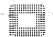
As shown in Figure 3, soldered ball 10 is provided at the zone in addition, lower surface center of substrate 7, have fixed intervals, and each soldered ball 10 has the size the same with other soldered balls.
The pad 65 that has the position of a plurality of corresponding soldered balls on printed circuit board (PCB) 51 encapsulates 5 so that this BFA to be installed, and this pad 65 has the unified size corresponding with the size of soldered ball 10.
In addition, trace 70 is arranged on printed circuit board (PCB) 51, that is, wiring diagram is so that be electrically connected to the peripheral chip that is contained on the printed circuit board (PCB) 51 with BGA or CSP (chip-scale package).But, be difficult to this trace 70 is connected with the pad 65 that is positioned at printed circuit board (PCB) 51 medial region, because the width of 65 of pads is very narrow, many traces 70 are difficult for passing through.Therefore, under the situation of multilayer board 51, the way of through hole is made in suggestion in the pad 65 of printed circuit board (PCB) 51, and like this, via through holes connects trace 70 and inboard pad 65.
But because printed circuit board (PCB) 51 should have through hole, and the wiring pattern that is formed with the layer of through hole subsequently should be connected to the wiring pattern of the layer that this BGA encapsulation 5 or CSP are housed, and like this, it is complicated that the design of printed circuit board (PCB) has just become.In addition, if this through hole is not suitable for laying trace 70, the space that pad is 65 can be guaranteed by the size that reduces each pad 65, so that in this space, lay trace 70, but in this case, a problem is arranged, and the welded condition that soldered ball 10 and pad are 65 has reduced because be used for the scolder of connection pads 65 and soldered ball 10 with regard to no good cake.
Therefore, under the situation of the printed circuit board (PCB) 51 that a plurality of BGA or CSP are housed, be necessary in 65 spaces of guaranteeing to be scheduled to of pad.But this has reduced the integral level that peripheral chip is installed on printed circuit board (PCB) 51.
Summary of the invention
Therefore, an object of the present invention is to provide a kind of printed circuit board (PCB), make its simplicity of design, improve the integrated quantity of peripheral chip, and keep good welded condition.
Other purpose of the present invention and advantage portions below describe, and some part becomes clearly by explanation, maybe can invent and understand by implementing this.
These and other purpose of the present invention, can have the printed circuit board (PCB) that a plurality of correspondences are made in the pad of the welding pin on the semiconductor die package and realize by providing, this pad be made in edge local of contiguous printed circuit board (PCB) and has the rectangular shape that prolongs towards edge direction.
In one embodiment of the present of invention, the pad of the central area of contiguous printed circuit board (PCB) has been made circle.
One embodiment of the present of invention also have, and the area of rectangular pads and circular pad area are roughly the same.
Description of drawings
These and other purpose and the understanding and understand easily of becoming of will carrying out in conjunction with the drawings of advantage of the present invention for the explanation of embodiment.
Fig. 1 is the schematic section with chip of a plurality of pins;
Fig. 2 is the plane graph of printed circuit board (PCB) according to an embodiment of the invention; With
Fig. 3 is the plane graph of traditional printed circuit board (PCB).
Embodiment
Below will be in detail with reference to detailed embodiment in conjunction with the accompanying drawings of the present invention, wherein the label of similar elements is consistent.Following embodiment is of the present invention in order to explain in conjunction with the accompanying drawings.
As shown in Figure 1, BGA (ball grid array) encapsulation, example as semiconductor die package is installed in according on the printed circuit board (PCB) of the present invention, consisting of of this printed circuit board (PCB), the substrate 7 that epoxy resin is made, the circuit pattern 8 that forms on substrate 7 is coated in the solder mask 9 on the circuit pattern 8, be contained in the semiconductor chip 3 at substrate 7 centers and the lead 4 that circuit pattern 8 and this semiconductor chip 3 are electrically connected.This semiconductor chip 3 and lead 4 linings are stamped one deck resin bed 6 in case oxidation and corrosion.
Have a plurality of soldered ball 10 as welding pin at the lower surface in the face of the substrate 7 of printed circuit board (PCB) 1 (with reference to Fig. 2), they are electrically connected with this substrate 7.Soldered ball 10 is made in predetermined interval on the zone beyond the central area on the lower surface of substrate 7 to form a plurality of row and columns.At this, each soldered ball 10 is hemispherical and has the same dimensions as each other.
As shown in Figure 2, on printed circuit board (PCB) 1, have a plurality of pads 15 so that BGA encapsulation 5 and corresponding with the position of soldered ball 10 to be installed.The same with soldered ball 10, pad 15 is placed in predetermined interval and is positioned on the printed circuit board (PCB) 1 on the zone in addition, central area to form a plurality of row and columns.
In pad 15, the pad 16 of the center of contiguous printed circuit board (PCB) 1 is similarly circular with traditional pad 65, and the pad 17 at the edge of contiguous printed circuit board (PCB) 1 is a rectangle.This rectangular pads 17 mind-set edge from this printed circuit board (PCB) 1 extends, and preferably the gross area with circular pad 16 is identical respectively.Therefore, the width between this rectangular pads 17 is greater than the width of 16 of circular pad.
Therefore, because the width between the pad 17 has increased at the fringe region of this printed circuit board (PCB), enough spaces of trace 20 have been guaranteed to lay 17 of rectangular pads.At this, trace 20 links together this printed circuit board (PCB) 1 by the pad 15 that is connected to separately with peripheral chip.In addition, because this rectangular pads 17 equals circular pad 16 on area, soldered ball 10 is in the welded condition of each rectangular pads 17 and welded condition equivalence in each circular pad 16.
On the other hand, when the row separately of this rectangular pads 17 meets in the angular region, owing to lay trace 20 enough spaces are arranged, so still can provide circular pad 16.
As previously mentioned, according to the present invention, have a plurality of pins for example on the printed circuit board (PCB) 1 of the BGA encapsulation of soldered ball 10 or CSP having installed, the pad 16 of the central area of adjoining plate has the circle of similar traditional pad 65, and the pad 17 at the edge of adjoining plate is a rectangle.Therefore, the space of laying the trace 20 of the pad 16 that connects contiguous central area is guaranteed, and need not form through hole, has so just realized the simple designs for printed circuit board (PCB), and has improved on this printed circuit board (PCB) 1 integrated level to peripheral chip.
In the above-described embodiments, the pad 16 of the central area of adjoining plate is circular, but also can be the rectangle of the pad 17 at the edge of adjoining plate, or other have the shape of function of the present invention.
As previously mentioned,, provide a kind of printed circuit board (PCB), can reach simple designs, improve the integrated level that peripheral chip is installed, and guarantee welded condition according to the present invention.
Although announcement has also been described some embodiments of the present invention, under the condition that does not break away from principle of the present invention and spirit, these those skilled in the art can make amendment to embodiments of the invention.
Claims (13)
1. a printed circuit board (PCB) has a plurality of pads corresponding to the welding pin on semiconductor die package,
Described pad is made in the edge of contiguous described printed circuit board (PCB), and has the rectangular shape that extends along towards the direction at edge; And
The area of each described rectangular pads is substantially equal to the area of the pad of each central area that is close to described printed circuit board (PCB),
Wherein said rectangular pads distributes along a plurality of sides straight line at edge, and some pads that its straight line meets in the corner at edge have round-shaped.
2. printed circuit board (PCB) according to claim 1, wherein said semiconductor die package are the BGA encapsulation.
3. printed circuit board (PCB) according to claim 1, some pads in the pad of the central area of the described printed circuit board (PCB) of wherein said vicinity have round-shaped.
4. printed circuit board (PCB) according to claim 3, wherein the area of each described rectangular pads is substantially equal to the area of each described circular pad.
5. printed circuit board (PCB) according to claim 3, wherein the described rectangular pads on this printed circuit board (PCB) is round circular pad.
6. printed circuit board (PCB) according to claim 3, wherein said rectangular pads distributes along a plurality of sides straight line at edge, and some pads that its straight line meets in the corner at edge have round-shaped.
7. printed circuit board (PCB) according to claim 3 further comprises the trace that extends to the edge of this printed circuit board (PCB) from described each circular pad between the adjacent pads of described rectangular pads.
8. printed circuit board (PCB) according to claim 3, wherein said rectangular pads form the many lines that are parallel to each a plurality of side at edge.
9. printed circuit board (PCB) according to claim 3, the width between the wherein said rectangular pads is greater than the width between the described circular pad.
10. printed circuit board (PCB) according to claim 1, the width between the wherein said rectangular pads is greater than the width between the described circular pad.
11. an equipment comprises:
Semiconductor die package, described semiconductor die package comprises:
Substrate has a plurality of roughly the same welding pin of size that are positioned on its first surface,
Be located at the circuit pattern on the second surface of described first surface reverse side substrate,
Be located at the semiconductor chip on this second surface,
Lead is used to connect this semiconductor chip and described circuit pattern; With
Printed circuit board (PCB) comprises:
The pad of a plurality of positions corresponding to welding pin, some said pads are positioned at the edge of this printed circuit board (PCB) and have the rectangular shape that extends along towards the direction at edge,
The pad of wherein said rectangular shape distributes along a plurality of sides straight line at edge, and some pads that its straight line meets in the corner at edge have round-shaped.
12. equipment according to claim 11, some pads in the pad of the central area of the described printed circuit board (PCB) of wherein said vicinity have round-shaped.
13. equipment according to claim 12, wherein each described rectangular pads roughly has and each described circular pad area identical.
Applications Claiming Priority (2)
| Application Number | Priority Date | Filing Date | Title |
|---|---|---|---|
| KR10-2001-0041547A KR100416000B1 (en) | 2001-07-11 | 2001-07-11 | Pcb mounting chip having plural pins |
| KR41547/2001 | 2001-07-11 |
Publications (2)
| Publication Number | Publication Date |
|---|---|
| CN1396799A CN1396799A (en) | 2003-02-12 |
| CN1248552C true CN1248552C (en) | 2006-03-29 |
Family
ID=19712044
Family Applications (1)
| Application Number | Title | Priority Date | Filing Date |
|---|---|---|---|
| CNB021222908A Expired - Fee Related CN1248552C (en) | 2001-07-11 | 2002-06-04 | Printed circuit board with improved pad structure |
Country Status (3)
| Country | Link |
|---|---|
| US (1) | US7199478B2 (en) |
| KR (1) | KR100416000B1 (en) |
| CN (1) | CN1248552C (en) |
Families Citing this family (19)
| Publication number | Priority date | Publication date | Assignee | Title |
|---|---|---|---|---|
| DE10157362B4 (en) * | 2001-11-23 | 2006-11-16 | Infineon Technologies Ag | Power module and method for its production |
| JP2005166794A (en) * | 2003-12-01 | 2005-06-23 | Ricoh Co Ltd | Component package, printed wiring board and electronic apparatus |
| CN100369533C (en) * | 2004-01-18 | 2008-02-13 | 敦南科技股份有限公司 | Wire soldering method for circuit board package |
| KR100632469B1 (en) | 2004-04-20 | 2006-10-09 | 삼성전자주식회사 | Semiconductor chip package |
| CN1314509C (en) * | 2004-11-24 | 2007-05-09 | 广州金升阳科技有限公司 | Pad spot welding method |
| US7425684B2 (en) * | 2005-02-03 | 2008-09-16 | Sang Henry Ta | Universal systems printed circuit board for interconnections |
| US20060172614A1 (en) * | 2005-02-03 | 2006-08-03 | Ta Sang H | Universal systems printed circuit blocks and method for interconnecting the same |
| US7962232B2 (en) * | 2006-10-01 | 2011-06-14 | Dell Products L.P. | Methods and media for processing a circuit board |
| JP5049573B2 (en) * | 2006-12-12 | 2012-10-17 | 新光電気工業株式会社 | Semiconductor device |
| JP2009182104A (en) * | 2008-01-30 | 2009-08-13 | Toshiba Corp | Semiconductor package |
| FR2967328B1 (en) * | 2010-11-10 | 2012-12-21 | Sierra Wireless Inc | ELECTRONIC CIRCUIT COMPRISING A FACE OF REPORT ON WHICH ARE AGENCIES OF CONTACT PLOTS |
| JP5842859B2 (en) * | 2013-04-15 | 2016-01-13 | 株式会社村田製作所 | Multilayer wiring board and module having the same |
| KR102041501B1 (en) * | 2013-09-13 | 2019-11-06 | 삼성전자 주식회사 | Array printed circuit board, method for replacing X-out printed circuit board of the same and electronic apparatus using the same |
| CN105188257B (en) * | 2015-08-31 | 2018-06-19 | 广东欧珀移动通信有限公司 | Circuit board and its electronic product and chip recognition methods |
| CN107612226B (en) * | 2017-10-31 | 2024-05-03 | 珠海格力电器股份有限公司 | Surface mounting structure, surface mounting method, motor and surface mounting chip |
| CN212064501U (en) * | 2020-03-13 | 2020-12-01 | 华为技术有限公司 | Circuit board structure and electronic equipment |
| CN112752398A (en) * | 2020-11-24 | 2021-05-04 | 广州朗国电子科技有限公司 | Chip bonding pad structure of PCB |
| CN114464585B (en) * | 2022-04-12 | 2022-07-12 | 飞腾信息技术有限公司 | Semiconductor substrate, semiconductor device, integrated circuit system and electronic equipment |
| CN114501849A (en) * | 2022-04-15 | 2022-05-13 | 北京万龙精益科技有限公司 | Improved design method of integrated circuit packaging bonding pad and bonding pad packaging library |
Family Cites Families (23)
| Publication number | Priority date | Publication date | Assignee | Title |
|---|---|---|---|---|
| US4720915A (en) * | 1986-03-25 | 1988-01-26 | True Grid, Ltd. | Printed circuit board and process for its manufacture |
| JPH04241676A (en) * | 1991-01-16 | 1992-08-28 | Nec Corp | Pattern data structure of printed wiring board |
| US5194137A (en) * | 1991-08-05 | 1993-03-16 | Motorola Inc. | Solder plate reflow method for forming solder-bumped terminals |
| US5340772A (en) * | 1992-07-17 | 1994-08-23 | Lsi Logic Corporation | Method of increasing the layout efficiency of dies on a wafer and increasing the ratio of I/O area to active area per die |
| US5593927A (en) * | 1993-10-14 | 1997-01-14 | Micron Technology, Inc. | Method for packaging semiconductor dice |
| US5557505A (en) * | 1994-07-22 | 1996-09-17 | Ast Research, Inc. | Dual pattern microprocessor package footprint |
| JPH08274425A (en) * | 1995-03-29 | 1996-10-18 | Sony Corp | Printed wiring board |
| US5829124A (en) * | 1995-12-29 | 1998-11-03 | International Business Machines Corporation | Method for forming metallized patterns on the top surface of a printed circuit board |
| KR20040108691A (en) * | 1996-01-11 | 2004-12-24 | 이비덴 가부시키가이샤 | Printed wiring board and method for manufacturing the same |
| JP2825085B2 (en) * | 1996-08-29 | 1998-11-18 | 日本電気株式会社 | Semiconductor device mounting structure, mounting board, and mounting state inspection method |
| JPH10290058A (en) * | 1997-04-16 | 1998-10-27 | Seiko Epson Corp | Printed-circuit board |
| JPH116103A (en) | 1997-06-18 | 1999-01-12 | Maeda Road Constr Co Ltd | Soil pavement material, soil pavement mechanism, and conditioning method for raw material for soil pavement |
| JPH1126919A (en) * | 1997-06-30 | 1999-01-29 | Fuji Photo Film Co Ltd | Printed wiring board |
| US6333565B1 (en) * | 1998-03-23 | 2001-12-25 | Seiko Epson Corporation | Semiconductor device and method of manufacturing the same, circuit board, and electronic instrument |
| US6316736B1 (en) * | 1998-06-08 | 2001-11-13 | Visteon Global Technologies, Inc. | Anti-bridging solder ball collection zones |
| US6118182A (en) | 1998-06-25 | 2000-09-12 | Intel Corporation | Integrated circuit package with rectangular contact pads |
| JP2000077819A (en) * | 1998-08-31 | 2000-03-14 | Toshiba Corp | Printed board and electronic unit |
| JP2000244106A (en) | 1998-12-25 | 2000-09-08 | Ibiden Co Ltd | Board for mounting electronic components |
| JP2000208909A (en) | 1999-01-12 | 2000-07-28 | Nec Home Electronics Ltd | Printed board |
| JP2000223653A (en) * | 1999-02-02 | 2000-08-11 | Rohm Co Ltd | Semiconductor device having chip-on-chip structure and semiconductor chip using the same |
| KR100347949B1 (en) * | 1999-11-27 | 2002-08-09 | 엘지전자주식회사 | A structure of solder land for component mounting |
| US20020144397A1 (en) * | 2000-01-21 | 2002-10-10 | Morris Terrel L. | Subtractive process for fabricating cylindrical printed circuit boards |
| JP2001320154A (en) * | 2000-05-02 | 2001-11-16 | Satsuma Tsushin Kogyo Kk | Method of filling through hole board with hole-stopping liquid resin, and filling apparatus |
-
2001
- 2001-07-11 KR KR10-2001-0041547A patent/KR100416000B1/en not_active IP Right Cessation
-
2002
- 2002-05-29 US US10/156,016 patent/US7199478B2/en not_active Expired - Fee Related
- 2002-06-04 CN CNB021222908A patent/CN1248552C/en not_active Expired - Fee Related
Also Published As
| Publication number | Publication date |
|---|---|
| US7199478B2 (en) | 2007-04-03 |
| CN1396799A (en) | 2003-02-12 |
| KR20030006008A (en) | 2003-01-23 |
| US20030011074A1 (en) | 2003-01-16 |
| KR100416000B1 (en) | 2004-01-24 |
Similar Documents
| Publication | Publication Date | Title |
|---|---|---|
| CN1248552C (en) | Printed circuit board with improved pad structure | |
| CN101370352B (en) | Printed circuit board and its production method, and a ball grid array bonding pad pattern | |
| JPH11297889A (en) | Semiconductor package, mounting board and mounting method by use of them | |
| US5450289A (en) | Semiconductor package and a printed circuit board applicable to its mounting | |
| US20100052186A1 (en) | Stacked type chip package structure | |
| US7180182B2 (en) | Semiconductor component | |
| US5324985A (en) | Packaged semiconductor device | |
| US6320249B1 (en) | Multiple line grids incorporating therein circuit elements | |
| KR100850286B1 (en) | Semiconductor chip package attached electronic device and integrated circuit module having the same | |
| US8283790B2 (en) | Electronic device | |
| US5946195A (en) | Semiconductor device, method of making the same and mounting the same, circuit board and flexible substrate | |
| JP3330468B2 (en) | Wiring board and semiconductor device | |
| US20030080418A1 (en) | Semiconductor device having power supply pads arranged between signal pads and substrate edge | |
| KR100233864B1 (en) | Input and output bump forming method of area array bumped semiconductor package using lead frame | |
| US20070209830A1 (en) | Semiconductor chip package having a slot type metal film carrying a wire-bonding chip | |
| US20240304534A1 (en) | Thermally improved substrate structure and package assembly with the same | |
| CN1707766A (en) | Method for preventing semiconductor assembly pin welding from shorting circuit | |
| KR100367729B1 (en) | Multiple line grid array package | |
| US20230337359A1 (en) | Circuit board and circuit module | |
| JP4523425B2 (en) | Semiconductor device mounting substrate | |
| US7939951B2 (en) | Mounting substrate and electronic apparatus | |
| KR940003374B1 (en) | Package of semiconductor device | |
| JPH02138766A (en) | Package structure of electronic component | |
| US20120025376A1 (en) | Ball grid array package | |
| KR100344648B1 (en) | Land Grid Array(LGA) package |
Legal Events
| Date | Code | Title | Description |
|---|---|---|---|
| C10 | Entry into substantive examination | ||
| SE01 | Entry into force of request for substantive examination | ||
| C06 | Publication | ||
| PB01 | Publication | ||
| C10 | Entry into substantive examination | ||
| SE01 | Entry into force of request for substantive examination | ||
| C14 | Grant of patent or utility model | ||
| GR01 | Patent grant | ||
| CF01 | Termination of patent right due to non-payment of annual fee |
Granted publication date: 20060329 Termination date: 20160604 |