CN115662926A - Automatic slotting equipment, slotting method and full-cutting system - Google Patents
Automatic slotting equipment, slotting method and full-cutting system Download PDFInfo
- Publication number
- CN115662926A CN115662926A CN202211690556.9A CN202211690556A CN115662926A CN 115662926 A CN115662926 A CN 115662926A CN 202211690556 A CN202211690556 A CN 202211690556A CN 115662926 A CN115662926 A CN 115662926A
- Authority
- CN
- China
- Prior art keywords
- wafer assembly
- assembly
- wafer
- slotting
- cleaning
- Prior art date
- Legal status (The legal status is an assumption and is not a legal conclusion. Google has not performed a legal analysis and makes no representation as to the accuracy of the status listed.)
- Granted
Links
Images


Classifications
-
- Y—GENERAL TAGGING OF NEW TECHNOLOGICAL DEVELOPMENTS; GENERAL TAGGING OF CROSS-SECTIONAL TECHNOLOGIES SPANNING OVER SEVERAL SECTIONS OF THE IPC; TECHNICAL SUBJECTS COVERED BY FORMER USPC CROSS-REFERENCE ART COLLECTIONS [XRACs] AND DIGESTS
- Y02—TECHNOLOGIES OR APPLICATIONS FOR MITIGATION OR ADAPTATION AGAINST CLIMATE CHANGE
- Y02P—CLIMATE CHANGE MITIGATION TECHNOLOGIES IN THE PRODUCTION OR PROCESSING OF GOODS
- Y02P70/00—Climate change mitigation technologies in the production process for final industrial or consumer products
- Y02P70/50—Manufacturing or production processes characterised by the final manufactured product
Landscapes
- Container, Conveyance, Adherence, Positioning, Of Wafer (AREA)
Abstract
The invention discloses automatic slotting equipment, a slotting method and a full-cutting system, which belong to the field of semiconductor processing and comprise the following steps: a feeding device; the cleaning device is used for cleaning the wafer assembly; a coating device for coating the wafer assembly; the first conveying device can convey the wafer assembly back and forth among the feeding device, the cleaning device and the coating device and is provided with a buffer station; the slotting device is used for slotting the wafer assembly; the second carrying device can carry the wafer assembly back and forth between the buffer storage station and the slotting device; the second conveying device comprises a first conveying mechanism and a second conveying mechanism, and the moving directions of the first conveying mechanism and the second conveying mechanism are opposite. The first carrying device can directly carry the wafer assembly from the feeding device to the cleaning device or the coating device, and the transfer is simple and the efficiency is high; the second carrying device comprises a first carrying mechanism and a second carrying mechanism, so that the wafer assembly taking and placing efficiency is improved.
Description
Technical Field
The invention relates to the technical field of semiconductor processing, in particular to automatic slotting equipment, a slotting method and a full-cutting system.
Background
The semiconductor industry has developed rapidly in recent years and demand continues to increase annually. Wafers are used as base materials in the semiconductor industry, and the yield and efficiency in the processing process are particularly important.
Chinese utility model CN210209046U discloses a full-automatic laser beam machining equipment, including material platform station, the coating station, the machining station, wash the station, transport mechanism, and go up unloading mechanism, material platform station is used for depositing the work piece around the processing, the coating station is used for carrying out the coating operation to the work piece of placing above that, the machining station is used for carrying out the laser beam machining operation to the work piece after placing the coating above that, wash the station and be used for carrying out the washing operation to the work piece after the laser beam machining of placing above that, transport mechanism is used for setting up at the coating station, between machining station and the washing station, with the work piece transfer to the machining station after coating on the coating station, perhaps transfer the work piece after the laser beam machining on the machining station to washing station. The feeding and discharging station is located between the material platform station and the cleaning station so as to transfer the cleaned workpiece on the cleaning station to the material platform station, or transfer the workpiece to be machined on the material platform station to the cleaning station, and then the conveying mechanism transfers the workpiece to be machined on the cleaning station to the coating station for coating.
However, with the above structure, when the workpiece is transferred from the material platform station to the coating station, the loading and unloading mechanism is required to transfer the workpiece from the material platform station to the cleaning station first, and then the conveying mechanism transfers the workpiece on the cleaning station to the coating station for coating, so that the transfer operation is complicated and time-consuming; in addition, when the conveying mechanism works, the workpieces can only be transferred one by one, for example, after the workpieces on the processing station are transferred to the cleaning station, the workpieces on the cleaning station can be transferred to the material platform station, the transfer efficiency is low, and the overall efficiency of the slotting equipment is low.
Accordingly, there is a need for improvements in the art that overcome the deficiencies in the prior art.
Disclosure of Invention
The invention aims to provide automatic slotting equipment, a slotting method and a full-cutting system so as to improve the transfer efficiency of wafers.
The purpose of the invention is realized by the following technical scheme: an automatic grooving apparatus comprising: the feeding device is used for storing the wafer assembly; the cleaning device is used for cleaning the wafer assembly; a coating device for coating the wafer assembly; a first conveying device capable of conveying the wafer assembly to and fro among the loading device, the cleaning device and the coating device, wherein the first conveying device is provided with a buffer storage station; the slotting device is used for slotting the wafer assembly; the second carrying device can carry the wafer assembly back and forth between the buffer storage station and the slotting device; the second conveying device comprises a first conveying mechanism and a second conveying mechanism, and the moving directions of the first conveying mechanism and the second conveying mechanism are opposite.
Further, loading attachment places the platform including being used for placing the wafer box, it includes to place the platform: the storage bin is provided with a taking and placing inlet at one side facing the first carrying device, and a taking and placing outlet at one side opposite to the taking and placing inlet; the placing plate is connected in the storage bin in a sliding mode and can be pulled out of the storage bin through the placing outlet.
Furthermore, the two sides of the storage bin in the sliding direction of the placing plate are respectively provided with a first abutting piece and a second abutting piece, the placing plate is provided with a third abutting piece limited between the first abutting piece and the second abutting piece, the third abutting piece and the first abutting piece are in magnetic attraction fit, and the third abutting piece and the second abutting piece are in magnetic attraction fit.
Further, the feeding device, the cleaning device and the coating device are arranged along the X-axis direction, the first carrying device comprises a grabbing mechanism which can reciprocate among the feeding device, the cleaning device and the coating device along the X-axis direction and pick and place wafer components, the feeding device comprises a lifting mechanism in transmission connection with the placing table, and the lifting mechanism is suitable for driving the placing table to lift along the Z-axis direction.
Further, the first carrying device comprises a first bearing mechanism with the cache station, the first bearing mechanism is suitable for positioning the position of the wafer assembly in the Y-axis direction, and the grabbing mechanism, the first bearing mechanism and the cleaning device are sequentially arranged from top to bottom.
Furthermore, the grabbing mechanism comprises two clamping pieces for taking and placing the wafer assembly, wherein one of the clamping pieces faces the taking and placing inlet of the feeding device, and the other clamping piece faces away from the taking and placing inlet of the feeding device.
Further, the cleaning device includes: the cleaning device comprises a first shell, a second shell and a cleaning mechanism, wherein a cleaning cavity is formed in the first shell, and a first opening is formed in the top of the cleaning cavity; the first supporting platform mechanism comprises a first lifting component, a first rotating component arranged on the first lifting component and a first supporting platform which is arranged on the first rotating component and contained in the cleaning cavity, and the first supporting platform can extend out through the first opening; the first spray head mechanism is positioned in the cleaning cavity and comprises a cleaning spray head facing the first supporting table; the side wall of the cleaning cavity is provided with a first splash-proof structure for blocking cleaning liquid from flowing out of the first opening, and/or the first opening is provided with a sealing cover structure, and the sealing cover structure can be opened or closed to the first opening.
Further, the coating apparatus includes: the second shell is internally provided with a coating cavity, and the top of the coating cavity is provided with a second opening; a second supporting table mechanism which comprises a second rotating assembly and a second supporting table which is arranged on the second rotating assembly and is contained in the coating cavity, wherein the second supporting table can extend out through the second opening; the second bearing mechanism is positioned above the second shell, is suitable for positioning the position of the wafer assembly in the Y-axis direction, and can lift along the Z-axis direction; the second shell is of a lifting structure, and the second shell is in a descending state for driving the second supporting platform to be exposed out of the second opening and in an ascending state for driving the second supporting platform to be in the coating cavity.
Furthermore, a second splash-proof structure is arranged above the second bearing mechanism, and when the second shell is in a rising state, the second splash-proof structure covers the second opening.
Further, the first carrying mechanism and the second carrying mechanism are identical in structure, and the first carrying mechanism comprises: a second linear module; the second mounting frame comprises a mounting frame main body in transmission connection with the second linear module and at least two movable plates movably connected to the mounting frame main body; the plurality of taking and placing parts are used for taking and placing the wafer assembly and are respectively fixed on the two movable plates; the dustproof structure is positioned above the taking and placing part and can cover the wafer assembly at the taking and placing part; wherein the movable plate is movably adjusted relative to the mounting frame body along the radial direction of the wafer assembly.
Further, the slotting device comprises: the translation mechanism can move along the X-axis direction and the Y-axis direction; the third support table mechanism is in transmission connection with the translation mechanism; the laser mechanism is arranged above the third support table mechanism and is positioned in the moving stroke range of the translation mechanism, and the laser mechanism comprises a laser, a third lifting component and a dust collection component, wherein the third lifting component drives the laser to lift along the Z-axis direction; the dust collection assembly comprises a dust collection main machine for providing adsorption force and a dust collection head communicated with the dust collection main machine, wherein the dust collection head is arranged at a laser emitting part of the laser and can synchronously lift along with the laser.
Further, the third support table mechanism includes: the third supporting platform is used for supporting the wafer of the wafer assembly; the supporting assembly is arranged at the outer edge of the third supporting table and used for supporting the tool of the wafer assembly; wherein the support assembly can be expanded or contracted along the radial direction of the third support platform.
Further, the support assembly includes: a connecting rod fixed to an outer periphery of the third support table in a radial direction of the third support table; the supporting block is sleeved on the connecting rod and can move along the axial direction of the connecting rod; a locking structure provided on the support block and having a locked state that restricts axial movement of the support block along the connecting rod and an unlocked state that is restricted from unlocking, the locking structure being switched from the locked state to the unlocked state in response to a pressing operation and being adapted to be reset from the unlocked state to the locked state when the pressing is released.
In addition, the invention also provides a slotting method, which comprises the automatic slotting equipment, and comprises the following steps: s1: the first carrying device moves to the pick-and-place position of the feeding device to take out the wafer assembly to be grooved, and the wafer assembly is moved to a caching station; s2: the cleaning device receives the wafer assembly at the cache station for cleaning, and returns the wafer assembly to the cache station after cleaning; s3: the first carrying device continuously moves the wafer assembly to a coating station of the coating device, and the coating device receives the wafer assembly to coat the wafer assembly with the protective liquid and returns the wafer assembly to the coating station after coating is finished; s4: the first carrying device moves the wafer assembly back to the caching station, the first carrying mechanism of the second carrying device moves the wafer assembly to the slotting device for slotting, and meanwhile, the second carrying mechanism of the second carrying device moves the wafer assembly after slotting on the slotting device back to the caching station; s5: the cleaning device receives the wafer assembly after the buffer station is slotted and cleans the wafer assembly again, and the first carrying device moves the slotted and cleaned wafer assembly back to the feeding device.
Further, when the wafer assembly is transferred between the cache station and the feeding device, the wafer assembly is clamped towards a clamping piece of the feeding device through the first carrying device; when the wafer assembly is transferred between the cache station and the coating station, the wafer assembly is clamped by the clamping piece of the first carrying device, which faces away from the feeding device.
In addition, the invention also provides a full cutting system which comprises the automatic slotting equipment.
Compared with the prior art, the invention has the following beneficial effects: according to the invention, the first conveying device which is used for receiving the components among the feeding device, the cleaning device and the coating device is arranged, the first conveying device can directly convey the wafer components from the feeding device to the cleaning device or the coating device, the transfer operation is simple, no transfer structure is adopted, and the efficiency is high; in addition, the second carrying device comprises a first carrying mechanism and a second carrying mechanism which are opposite in moving direction, when one carrying mechanism takes out the processed wafer assembly from the slotting device and moves to the caching station, the other carrying mechanism can take out the wafer assembly to be processed from the caching station and moves to the slotting device at the same time, waiting is not needed, the picking and placing efficiency of the wafer assembly is improved, and the processing efficiency of the whole slotting device is improved.
Drawings
Fig. 1 is a schematic structural view of the automatic grooving apparatus of the present invention.
FIG. 2 is a schematic view showing the structure of the loading device, the first carrying device, the cleaning device and the coating device of the present invention.
FIG. 3 is a schematic view of a wafer assembly according to the present invention.
Fig. 4 is a schematic structural diagram of the feeding device in the invention.
FIG. 5 is a schematic view of the internal structure of the placing table of the present invention.
Fig. 6 is a schematic view of the structure of fig. 5 with the placement plate removed.
FIG. 7 is a schematic view of the placement table of the present invention.
Fig. 8 is a schematic structural view of the first carrying device in the present invention.
Fig. 9 is a schematic structural diagram of a first translation assembly of the present invention.
Fig. 10 is a schematic view of the cleaning apparatus of the present invention with the first opening open.
FIG. 11 is a schematic cross-sectional view of the cleaning device of the present invention with the first opening closed.
FIG. 12 is a schematic view of the structure of the coating apparatus of the present invention.
Fig. 13 is a front view schematically showing a coating apparatus of the present invention.
Figure 14 is a schematic view of the applicator device of the present invention with a second splash guard arrangement.
Fig. 15 is a schematic structural view of a second carrying device in the present invention.
Fig. 16 is a schematic view of the second mounting frame and the pick-and-place member according to the present invention.
Fig. 17 is a schematic structural view of the slotting device in the invention.
FIG. 18 is a schematic view of the third supporting table mechanism according to the present invention.
Fig. 19 is a schematic structural view of the support assembly of the present invention.
Fig. 20 is an exploded view of the support assembly of the present invention.
Figure 21 is a cross-sectional schematic view of a support assembly of the present invention.
Fig. 22 is a schematic view of the structure of the laser mechanism of the present invention.
Figure 23 is a schematic view of the construction of a cleaning head according to the invention.
Description of reference numerals:
100. a feeding device; 110. a lifting mechanism; 120. a placing table; 121. a storage bin; 122. a pick-and-place entrance; 123. a taking and placing outlet; 124. a first slide rail; 125. a first abutting member; 126. a second holding member; 127. a first removable cover; 131. positioning a block; 132. a positioning column; 140. placing a plate; 141. a third abutting member; 142. a handle; 143. a first placing block; 144. a second placing block; 145. a third placing block; 200. a first carrying device; 210. a first mounting bracket; 220. a grabbing mechanism; 221. a first linear module; 222. a connecting member; 223. a clamping member; 230. a first bearing mechanism; 231. a first support rail; 232. a second support rail; 233. a first translation assembly; 2331. a support; 2332. a drive motor; 2333. a transmission belt; 2334. a driving wheel; 2335. a driven wheel; 2336. connecting blocks; 300. a cleaning device; 310. a first housing; 311. a cleaning chamber; 312. a first opening; 320. a first support table mechanism; 321. a first lifting assembly; 322. a first rotating assembly; 323. a first support table; 324. a clamping block; 330. a first nozzle mechanism; 331. cleaning the swing arm; 332. cleaning the spray head; 340. a first splash guard structure; 350. a capping structure; 400. a coating device; 410. a second bearing mechanism; 411. a second lifting assembly; 412. a second translation assembly; 413. a third support rail; 414. a fourth support rail; 420. a second support table mechanism; 421. a second rotating assembly; 422. a second support table; 430. a second housing; 431. a coating chamber; 432. a second opening; 440. a second nozzle mechanism; 441. coating a spray head; 450. a second splash guard structure; 451. a main body portion; 452. a second removable cover; 500. a second carrying device; 510. a first carrying mechanism; 520. a second carrying mechanism; 511. a second linear module; 512. a second mounting bracket; 5121. a mounting bracket main body; 5122. a movable plate; 5123. a second slide rail; 5124. a slider; 5125. a fastener; 5126. a stopper; 513. a taking and placing part; 514. a dust-proof structure; 600. a slotting device; 610. a translation mechanism; 611. a third translation assembly; 612. a fourth translation assembly; 620. a third support table mechanism; 630. a laser mechanism; 631. a third lifting assembly; 632. a laser; 6321. a laser emitting section; 633. a dust collection assembly; 634. a dust collection host; 635. a dust collection head; 6351. a dust suction chamber; 6352. a third opening; 6353. a fourth opening; 636. a dust collection pipeline; 640. a third support table; 641. a first support surface; 650. a support assembly; 651. a connecting rod; 652. a support block; 6521. a second support surface; 6522. a first connection hole; 6523. a second connection hole; 6524. an accommodating cavity; 653. a magnetic member; 654. a movable rod; 655. a locking block; 656. a resilient member; 700. a wafer assembly; 710. a wafer; 720. assembling; 730. a film.
Detailed Description
In order to make the aforementioned objects, features and advantages of the present application more comprehensible, embodiments accompanying figures are described in detail below. It is to be understood that the specific embodiments described herein are merely illustrative of the application and are not limiting of the application. It should be further noted that, for the convenience of description, only some of the structures related to the present application are shown in the drawings, not all of the structures. All other embodiments, which can be derived by a person skilled in the art from the embodiments given herein without making any creative effort, shall fall within the protection scope of the present application.
The terms "comprising" and "having," as well as any variations thereof, in this application are intended to cover non-exclusive inclusions. For example, a process, method, system, article, or apparatus that comprises a list of steps or elements is not limited to only those steps or elements but may alternatively include other steps or elements not expressly listed or inherent to such process, method, article, or apparatus.
Reference herein to "an embodiment" means that a particular feature, structure, or characteristic described in connection with the embodiment can be included in at least one embodiment of the application. The appearances of the phrase in various places in the specification are not necessarily all referring to the same embodiment, nor are separate or alternative embodiments mutually exclusive of other embodiments. It is explicitly and implicitly understood by one skilled in the art that the embodiments described herein can be combined with other embodiments.
Referring to fig. 1 to 3, an automatic grooving apparatus according to a preferred embodiment of the present invention includes a feeding device 100, a first conveying device 200, a cleaning device 300, a coating device 400, a second conveying device 500, and a grooving device 600. The loading device 100 is used for storing the wafer assembly 700; the cleaning device 300 is used for cleaning the wafer assembly 700, and the coating device 400 is used for coating the wafer assembly 700; the first transfer device 200 may transfer the wafer assembly 700 to and from the loading device 100, the cleaning device 300, and the coating device 400; the slotting device 600 is used for slotting the wafer assembly 700; the second handling device 500 can shuttle the wafer assembly 700 between the first handling device 200 and the notching device 600.
Further, the wafer assembly 700 includes a wafer 710 and a tool 720 disposed at the periphery of the wafer 710, the tool 720 is an annular plate-shaped structure and disposed coaxially with the wafer 710, and the tool 720 and the wafer 710 are fixed together by a film 730 to reduce the possibility of damage to the wafer 710 during the handling, cleaning and coating processes, which will be described in detail later.
Further, referring to fig. 4 to 7, the feeding device 100 includes a lifting mechanism 110, a placing table 120 in transmission connection with the lifting mechanism 110, and a wafer cassette (not shown) detachably disposed on the placing table 120. The lifting mechanism 110 is a linear module disposed along the Z-axis direction, the placing stage 120 is fixedly connected to the moving portion of the lifting mechanism 110 to be lifted synchronously therewith, so as to drive the wafer assemblies 700 at different heights in the wafer cassette to be lifted to the pick-and-place positions, and the first transporting device 200 can be moved to the pick-and-place positions to pick out or place the wafer assemblies 700.
The table top of the placing table 120 is provided with a first positioning structure, and the wafer box is arranged on the table top of the placing table 120 and limited by the first positioning structure. The first positioning structure may be formed by a plurality of positioning blocks 131 and/or a plurality of positioning posts 132. The positioning blocks 131 may be disposed around the wafer cassette to cooperate with the positioning blocks to limit the positions of the wafer cassette in the X-axis and Y-axis directions, and/or the positioning posts 132 protrude from the top of the placing table 120 along the Z-axis direction, and positioning slots (not shown) are disposed on one side of the wafer cassette facing the positioning posts 132 and adapted to the positioning posts 132. In this embodiment, the first positioning structure is preferably a positioning block 131 and a positioning column 132, the positioning block 131 can quickly limit the position of the wafer box, so that the wafer box is accurately inserted into and matched with the positioning column 132, and the positioning column 132 can improve the connection tightness between the wafer box and the placing table 120, and improve the reliability of the wafer box and the placing table after installation.
Further, in order to improve the yield of the slotting equipment, the slotting equipment needs to detect the first slotted wafer 710 after being opened, so that the working condition of the equipment can be known, defects can be found timely, and the condition that the subsequent wafers 710 are slotted in batches is avoided. Preferably, in the present embodiment, a storage bin 121 for accommodating the first wafer assembly 700 is disposed in the placing stage 120, a pick-and-place inlet 122 is disposed on a side of the storage bin 121 facing the first transporting device 200, a pick-and-place outlet 123 is disposed on a side of the storage bin 121 opposite to the pick-and-place inlet 122, and the pick-and-place outlet 123 is communicated with the outside. The first transfer device 200 may take or put the wafer assembly 700 into or out of the access opening 122. When the first wafer inspection is required, the lifting mechanism 110 drives the placing table 120 to lift, so that the pick-and-place inlet 122 is located at the pick-and-place position, then the first transporting device 200 moves the grooved wafer assembly 700 from the pick-and-place inlet 122 into the storage bin 121, and the worker can take the wafer assembly 700 out of the storage bin 121 from the pick-and-place outlet 123 to inspect the wafer 710.
Preferably, the containing bin 121 is movably provided with a placing plate 140 for bearing the wafer assembly 700, the placing plate 140 can move along the X-axis direction and is pulled out of the containing bin 121 from the taking and placing outlet 123, so that the wafer assembly 700 can be conveniently taken out, the wafer 710 is prevented from being damaged in the process of taking out the wafer assembly 700 from the containing bin 121, normal operation of the first carrying device 200 is prevented from being influenced, non-stop wafer taking is realized, and the working efficiency is improved. Specifically, a first slide rail 124 is disposed on a bottom plate of the storage compartment 121 along the X-axis direction, and the bottom of the placement plate 140 is slidably connected to the first slide rail 124. The placing plate 140 has a first position and a second position, and when the placing plate 140 is located in the receiving chamber 121, the placing plate 140 is ensured to smoothly receive the wafer assembly 700; when in the second position, the wafer assembly 700 is outside the storage compartment 121 for the operator to remove the wafer assembly 700. Preferably, in order to ensure that the placing plate 140 reliably moves to the first position and the second position, a first abutting piece 125 and a second abutting piece 126 are respectively arranged on two sides of the bottom plate of the receiving bin 121 in the X-axis direction, the first abutting piece 125 is arranged near the taking and placing inlet 122, the second abutting piece 126 is arranged near the taking and placing outlet 123, a gap is formed between the bottom of the placing plate 140 and the bottom plate of the receiving bin 121, a third abutting piece 141 is fixedly arranged at the bottom of the placing plate 140, the third abutting piece 141 is arranged between the first abutting piece 125 and the second abutting piece 126, when the placing plate 140 is in the first position, the third abutting piece 141 abuts against the first abutting piece 125, and when the placing plate 140 is in the second position, the third abutting piece 141 abuts against the second abutting piece 126. Preferably, in order to prevent the placing plate 140 from moving relative to the storage compartment 121 in a natural state, in this embodiment, the third abutting member 141 and the first abutting member 125 are in magnetic attraction fit, and the third abutting member 141 and the second abutting member 126 are in magnetic attraction fit, specifically, the third abutting member 141 may be made of a magnetic conductive material, and the first abutting member 125 and the second abutting member 126 are both made of a magnetic material, or the third abutting member 141 is made of a magnetic material, and the first abutting member 125 and the second abutting member 126 are both made of a magnetic conductive material.
Since the taking and placing outlet 123 of the storage bin 121 directly contacts with the outside, preferably, in order to prevent dust, water stain and the like from the outside from polluting the storage bin 121 through the taking and placing outlet 123, a first movable cover 127 is hinged to the storage bin 121 at the taking and placing outlet 123, and the first movable cover 127 can rotate to open or close the taking and placing outlet 123. In addition, in order to apply a pulling force to the placing plate 140, a handle 142 is disposed on a side of the placing plate 140 close to the taking and placing outlet 123, and when the placing plate 140 needs to be pulled to the second position, the first movable cover 127 is turned over to open the taking and placing outlet 123, and then the first movable cover extends into the storage bin 121 through the taking and placing outlet 123 and captures the handle 142.
Further, the placing plate 140 is provided with a first placing block 143 for carrying the small-sized wafer assembly 700 and a second placing block 144 for carrying the large-sized wafer assembly 700. The number of the first placing blocks 143 is two and is distributed on two sides of the storage bin 121 along the Y-axis direction, the number of the second placing blocks 144 is two and is distributed on two sides of the storage bin 121 along the Y-axis direction, and the second placing blocks 144 are located outside the first placing blocks 143. The first placement block 143 and the second placement block 144 have an L-shaped cross section, and the cross section is perpendicular to the X-axis to limit the position of the tool 720 in the Y-axis direction. In addition, in order to limit the position of the wafer assembly 700 in the X-axis direction, a third placing block 145 is disposed on a side of the placing plate 140 away from the pick-and-place inlet 122, the third placing block 145 is located between the two first placing blocks 143 and/or the two second placing blocks 144, and when the wafer assembly 700 is placed on the first placing blocks 143 or the second placing blocks 144 in the X-axis direction, the tool 720 can abut against the third placing block 145 to accurately position the wafer assembly 700.
Further, the feeding device 100, the cleaning device 300, and the coating device 400 are sequentially arranged along the X-axis direction. Referring to fig. 8 and 9, the first handling device 200 includes a first mounting frame 210, a gripping mechanism 220 provided on the first mounting frame 210, and a first carrying mechanism 230. The grabbing mechanism 220, the first carrying mechanism 230 and the cleaning device 300 are sequentially arranged from top to bottom, the grabbing mechanism 220 can move along the X-axis direction to reciprocate among the loading device 100, the cleaning device 300 and the coating device 400 and pick and place the wafer assembly 700, the first carrying mechanism 230 is used for carrying the wafer assembly 700 grabbed by the grabbing mechanism 220 and positioning the wafer assembly 700 in the Y-axis direction, so that the cleaning device 300 can accurately receive the wafer assembly 700.
The grabbing mechanism 220 includes a first linear module 221, a connecting member 222 and a clamping member 223. The first linear module 221 is fixed on the first mounting frame 210 along the X-axis direction, one end of the connecting member 222 is fixedly connected to the moving end of the first linear module 221, the other end of the connecting member extends to the right above the cleaning device 300 along the Y-axis direction, and the clamping member 223 is disposed at the other end of the connecting member 222 and corresponds to the picking and placing position of the wafer cassette. When the first linear module 221 drives the connecting member 222 to move toward the pod, the clamp 223 may be in the pick-and-place position to pick and place the wafer assembly 700. The clamping member 223 may specifically clamp or loosen the edge of the tool 720 in a manner that a clamping cylinder cooperates with a clamping sheet, which is not described herein again.
Preferably, in the present embodiment, the number of the clamping members 223 is two, wherein one clamping member 223 faces the access opening 122 of the loading device 100, and the other clamping member 223 faces away from the access opening 122 of the loading device 100. Compared with the position only arranged at the position facing the feeding device 100, the moving stroke of the first linear module 221 can be reduced, the cost is reduced, the volume is reduced, and the efficiency is improved. Specifically, when the grabbing mechanism 220 moves the wafer assembly 700 from the loading device 100 to the cleaning device 300, the grabbing mechanism 220 may clamp the fixture 720 by facing the clamping member 223 of the loading device 100, and when it is required to move the wafer assembly 700 to the coating device 400, the grabbing mechanism 220 may clamp the fixture 720 by facing away from the clamping member 223 of the loading device 100, and since the clamping member 223 clamps the edge of the fixture 720, the moving stroke of the diameter size of the wafer assembly 700 may be reduced when the wafer assembly 700 is moved to the coating device 400.
The first supporting mechanism 230 includes a first supporting rail 231 and a second supporting rail 232 extending along the X-axis direction, the first supporting rail 231 and the second supporting rail 232 are disposed oppositely to cooperate with the supporting tool 720, at this time, the wafer 710 is in a suspended state, so as to avoid contacting with the first supporting mechanism 230, and reduce the probability of damage to the wafer 710. The cross sections of the first supporting rail 231 and the second supporting rail 232 are L-shaped, the cross sections are perpendicular to the X axis, and the first supporting rail 231 and the second supporting rail 232 cooperate to limit the position of the tool 720 in the Y axis direction.
Specifically, the first supporting mechanism 230 further includes a first translating assembly 233, and the first translating assembly 233 is in transmission connection with the first supporting rail 231 and the second supporting rail 232 respectively, so as to drive the first supporting rail 231 and the second supporting rail 232 to move towards or away from each other, thereby defining the position of the wafer assembly 700 in the Y-axis direction.
Further, a buffer station is disposed on the first supporting mechanism 230, the cleaning device 300 is located at the buffer station, and the cleaning device 300 can receive the wafer assembly 700 at the buffer station to clean the wafer assembly 700.
Referring to fig. 10 and 11, the cleaning apparatus 300 includes a first housing 310, a first support table mechanism 320, and a first head mechanism 330. A cleaning cavity 311 is formed in the first housing 310, a first opening 312 is formed at the top of the cleaning cavity 311 in the Z-axis direction, the inner dimension of the first opening 312 is larger than the outer dimension of the tool 720, and the wafer assembly 700 can enter the cleaning cavity 311 from the first opening 312.
The first supporting table mechanism 320 includes a first lifting component 321, a first rotating component 322, and a first supporting table 323, the first rotating component 322 is disposed on the first lifting component 321, the first supporting table 323 is disposed on the first rotating component 322, so as to drive the first supporting table 323 to lift along the Z-axis direction, and drive the first supporting table 323 to rotate around the Z-axis. The first lifting assembly 321 may specifically be configured to perform lifting movement by an air cylinder or an electric cylinder disposed along the Z-axis direction, and an output end of the air cylinder or the electric cylinder is connected to a frame body for mounting the first rotating assembly 322. First rotating assembly 322 may be rotated by a motor in conjunction with a turntable.
The first support platform 323 is located in the cleaning chamber 311, and the inner dimension of the first opening 312 is larger than the outer dimension of the first support platform 323, so as to ensure that the first support platform 323 can smoothly extend out of the first housing 310 from the first opening 312 and receive the wafer assembly 700 on the first supporting mechanism 230. When the cleaning apparatus 300 receives the wafer assembly 700, the first support platform 323 raises and supports the wafer assembly 700, then the first supporting mechanism 230 drives the first support rail 231 and the second support rail 232 to move back, and then the first support platform 323 lowers to drive the wafer assembly 700 to synchronously lower into the cleaning chamber 311. When it is required to move the wafer assembly 700 on the cleaning apparatus 300 back to the first supporting mechanism 230, the first supporting platform 323 drives the wafer assembly 700 to rise above the first supporting rail 231 and the second supporting rail 232, and then the first supporting rail 231 and the second supporting rail 232 move toward each other, and at the same time, the first supporting platform 323 descends to be reset, and the wafer assembly 700 is re-supported on the first supporting rail 231 and the second supporting rail 232.
The first supporting platform 323 is provided with a clamping block 324, and the clamping block 324 can rotate relative to the first supporting platform 323. The plurality of clamping blocks 324 are distributed at intervals along the circumferential direction of the first supporting platform 323, and the plurality of clamping blocks 324 can be matched with the clamping tool 720 to limit the radial and axial positions of the tool 720, namely, the wafer assembly 700 and the first supporting platform 323 are relatively fixed. Specifically, when the first support platform 323 rotates, the clamping block 324 may rotate to the top of the first support platform 323 under the action of centrifugal force, and the tool 720 may be abutted against the top of the top, so as to prevent the wafer 710 from being damaged due to direct contact with the clamping block 324, and when the first support platform 323 stops rotating, the clamping block 324 may release the tool 720, so as to prevent the wafer 710 from being taken or placed on the first support platform 323.
Further, the first nozzle mechanism 330 is located in the cleaning chamber 311, the first nozzle mechanism 330 includes a cleaning swing arm 331 capable of swinging around the Z-axis and a cleaning nozzle 332 disposed on the cleaning swing arm 331, the cleaning nozzle 332 faces the first support platform 323, the cleaning swing arm 331 can drive the cleaning nozzle 332 to move relative to the first support platform 323 so as to adjust the cleaning nozzle 332 to the optimal cleaning position, and meanwhile, the cleaning swing arm 331 can also move the cleaning nozzle 332 away from the position right above the first support platform 323 so as to avoid restricting the lifting of the first support platform 323. The cleaning swing arm 331 can be driven by a motor or a rotary cylinder to swing, and the invention is not described herein again.
Preferably, in order to prevent the cleaning liquid from splashing out of the first opening 312 during the cleaning process, a first splash guard structure 340 is disposed on a side wall of the cleaning chamber 311, and the first splash guard structure 340 is located on a side of the cleaning chamber 311 close to the first opening 312. The first splash guard structure 340 is disposed in a ring shape, and a projection of the first splash guard structure 340 in the Z-axis direction covers a part of the first opening 312 to block a part of the first opening 312. Through setting up first splashproof structure 340 in washing chamber 311, wafer subassembly 700 cleaning process, the washing liquid that has the filth through wafer 710 and/or frock 720 upper surface rebound can receive the blockking of first splashproof structure 340 to avoid the washing liquid to rebound again to wafer 710 after the lateral wall bounce of washing chamber 311, prevent secondary pollution, improve cleaning efficiency, also can improve the cleanliness around belt cleaning device 300 simultaneously, prevent to pollute other devices.
The first splash guard structure 340 is a sheet-like structure, and one side of the first splash guard structure 340 is fixedly connected to a sidewall of the washing chamber 311, and the other side extends toward the center of the washing chamber 311. First splashproof structure 340 can be along washing the week side of chamber 311 and distribute in succession or intermittently, when adopting continuous distribution structure, can ensure that the whole week side of first opening 312 all obtains effectively stopping, improves the splashproof effect, and when adopting intermittent distribution structure, first splashproof structure 340 is formed by the cooperation of the mutual independent splashproof piece of multi-disc, when easy to assemble, also can replace the splashproof piece that corresponds alone when first splashproof structure 340 damages, reduce the maintenance cost.
In addition, when the spraying speed of the first spraying head mechanism 330 is too fast, or the rotating speed of the first supporting platform 323 is too fast, there is still a case that a part of the cleaning liquid is splashed out from the first opening 312, and in order to further improve the splash-proof effect, in this embodiment, the cleaning device 300 further includes a cover structure 350, and the cover structure 350 is located at the first opening 312 and is used for opening or closing the first opening 312. By providing the capping structure 350, the first opening 312 can be completely capped, thereby preventing the cleaning solution from splashing out of the first opening 312 and/or water mist generated by the cleaning solution from flying out of the first opening 312.
Specifically, in this embodiment, the cover structure 350 is preferably a roller shutter capable of automatically retracting, and the roller shutter is made of a waterproof material, such as waterproof cloth, a flexible plastic sheet, and the like. The cover structure 350 is disposed at one side of the first opening 312, and the cover structure 350 has a rolled state and a rolled state, wherein when the cover structure 350 is in the rolled state, the first opening 312 is in the open state, and when the cover structure 350 is in the rolled state, the first opening 312 is in the closed state. By adopting the cover structure 350 of the rolling shutter structure, when the cover structure 350 is in a rolling state, the volume of the cover structure 350 can be effectively reduced, and the occupied space is reduced. The roller blind may be wound on a rotating shaft driven by a motor to rotate, and the roller blind may be wound or unwound by rotating the rotating shaft in forward or reverse directions. Indeed, in other embodiments, the cover structure 350 may also be a hard waterproof board that can automatically open and close the first opening 312.
Further, referring to fig. 12 to 14, the coating apparatus 400 may receive the wafer assembly 700 conveyed by the first conveying apparatus 200 to coat the wafer 710. The coating apparatus 400 includes a second carriage mechanism 410, a second support table mechanism 420 located below the second carriage mechanism 410, a second housing 430 for housing the second support table mechanism 420, and a second head mechanism 440 for ejecting the protective liquid to the second support table mechanism 420.
The second carrier mechanism 410 has a coating station to which the first handling device 200 can handle the wafer assembly 700. The second carrier mechanism 410 is adapted to take the wafer assembly 700 out of or into the second support table mechanism 420.
Specifically, the second supporting mechanism 410 includes a second lifting assembly 411, a second translating assembly 412, a third supporting rail 413 and a fourth supporting rail 414. The second translation assembly 412 is disposed on the second lifting assembly 411, and the second lifting assembly 411 can drive the second translation assembly 412 to lift along the Z-axis direction. The structure of the second lifting assembly 411 is similar to that of the first lifting assembly 321, and the present invention is not repeated herein, and the second translation assembly 412 is mounted on the frame body of the second lifting assembly 411.
The third support rail 413 and the fourth support rail 414 are disposed opposite to each other to cooperate with the carrier wafer 710. The third support rail 413 and the fourth support rail 414 have similar structures to the first support rail 231 and the second support rail 232, and the description of the present invention is omitted. The second translation assembly 412 has the same structure as the first translation assembly 233, and is in transmission connection with the third support rail 413 and the fourth support rail 414 respectively, so as to drive the third support rail 413 and the fourth support rail 414 to move towards or away from each other, thereby defining the position of the wafer assembly 700 in the Y-axis direction and ensuring that the second support table mechanism 420 accurately receives the wafer assembly 700.
The second supporting table mechanism 420 includes a second rotating assembly 421 and a second supporting table 422 disposed on the second rotating assembly 421, the second supporting table 422 is used for receiving the wafer assembly 700 on the second bearing mechanism 410, and the structure of the second rotating assembly 421 is similar to that of the first rotating assembly 322 so as to drive the second supporting table 422 to rotate around the Z-axis. The structure of the second support platform 422 is the same as that of the first support platform 323, and a clamping block 324 is also provided thereon to tightly support the tool 720 of the wafer assembly 700 during the rotation of the second support platform 422.
A coating chamber 431 for accommodating the second support table 422 is formed in the second housing 430, a second opening 432 is formed at the top of the coating chamber 431 in the Z-axis direction, and the inner contour dimension of the second opening 432 is larger than the outer contour dimension of the tool 720. The second housing 430 can be lifted and lowered along the Z-axis direction, and may be implemented by an air cylinder or an electric cylinder. The second housing 430 has a descending state for driving the second supporting platform 422 to be exposed from the second opening 432 and an ascending state for driving the second supporting platform 422 to be completely located in the coating chamber 431, when the second housing 430 is in the descending state, it can avoid limiting the second supporting mechanism 410 from placing the wafer assembly 700 on the second supporting platform 422, and when the second housing 430 is in the ascending state, it can block the wafer assembly 700, and reduce the splashing amount of the protection liquid. When the wafer assembly 700 is received by the coating apparatus 400, the second housing 430 is lowered to a lowered state, the second lifting assembly 411 is lowered to support the wafer assembly 700 on the second support stage 422, then the second translation assembly 412 drives the third support rail 413 and the fourth support rail 414 to move back and forth away from the wafer assembly 700, and then the second housing 430 is raised to a raised state, so that the wafer assembly 700 is placed in the coating chamber 431. When it is desired to move the wafer assembly 700 on the coating apparatus 400 back to the second carrier mechanism 410, the reverse action is required.
Further, the second head mechanism 440 has the same structure as the first head mechanism 330, and includes a coating head 441 facing the second support stage 422 to spray the wafer 710 with the protective solution. When the second housing 430 is in the raised state, the coating head 441 is housed in the coating chamber 431.
Preferably, in order to avoid the protective liquid from splashing out of the second opening 432 during the coating process, a second splash guard structure 450 is provided above the second carrier mechanism 410, and the second splash guard structure 450 covers the second opening 432 when the second housing 430 is in the raised state. In this embodiment, the second splash guard 450 is specifically a fixed cover, and at least a part of the second splash guard is made of a transparent material, so that an operator can observe the coating condition in the coating process, and thus the problem existing in the coating process can be found in time, and the yield can be improved. Preferably, the second splash guard structure 450 includes a main body portion 451 and a second removable cover 452 movably coupled to the main body portion 451, the second removable cover 452 facing the second opening 432 and being movable relative to the main body portion 451 to open or close the second opening 432. The second flap 452 may be a sliding fit or a hinged fit with the body portion 451, and in this embodiment, a hinged fit is preferred so as to reduce the occupied space after the second flap 452 is opened. And through setting up second removable cover 452, when meetting emergency in the coating process, the operation personnel can open second opening 432 manually to stretch into and operate in coating chamber 431, improve operating efficiency.
Preferably, in order to prevent the coating nozzle 441 from being clogged due to long standby, the coating apparatus 400 further includes a wetting mechanism (not shown) having a water tank in which the liquid is stored, and when the coating nozzle 441 is completely sprayed, the coating nozzle 441 may be moved toward the wetting mechanism and immersed in the liquid to prevent the protective liquid on the coating nozzle 441 from being solidified. In this embodiment, the wetting mechanism is preferably fixed to the second housing 430 and is lifted and lowered synchronously with the second housing 430, and when the coating head 441 moves to the wetting mechanism, the second housing 430 can lift the wetting mechanism to immerse the coating head 441 in the liquid, thereby simplifying the structure of the wetting mechanism.
Further, referring to fig. 15 and 16, the second handling device 500 includes a first handling mechanism 510 and a second handling mechanism 520 for handling the wafer assembly 700 back and forth between the buffer storage station and the slotting device 600, when in operation, the moving directions of the first handling mechanism 510 and the second handling mechanism 520 are opposite, so that when one of the first handling mechanisms takes out the processed wafer assembly 700 from the slotting device 600 and moves to the buffer storage station, the other handling mechanism can simultaneously take out the wafer assembly 700 to be processed from the buffer storage station and move to the slotting device 600, and waiting is not needed, thereby improving the pick-and-place efficiency of the wafer assembly 700 and the processing efficiency of the whole slotting equipment.
Specifically, the first carrying mechanism 510 and the second carrying mechanism 520 have the same structure, and taking the first carrying mechanism 510 as an example, the first carrying mechanism 510 includes a second linear module 511, a second mounting bracket 512 fixedly connected to a moving end of the second linear module 511, and a pick-and-place member 513 disposed on the second mounting bracket 512.
The pick-and-place element 513 is embodied as a vacuum chuck that is attached to the upper surface of the tool 720 and/or the wafer 710. In this embodiment, the pick-and-place element 513 preferably contacts the tool 720 of the wafer assembly 700 to prevent damage to the wafer 710. The number of the taking and placing parts 513 is multiple, and the taking and placing parts are distributed along the circumferential direction of the tool 720 to be respectively in contact with multiple positions of the tool 720, so that the adsorption reliability is improved. Since the sizes of the wafers 710 vary, the sizes of the tools 720 vary accordingly, and preferably, in order to improve the versatility of the first carrying mechanism 510, the second mounting frame 512 can be adjusted along the radial direction of the wafer assembly 700, and the relative positions of the pick-and-place members 513 can be adjusted, so as to ensure that the pick-and-place members 513 can always contact with the upper surface of the tools 720 when replacing the wafers 710 with different sizes.
The second mounting frame 512 comprises a mounting frame body 5121 and at least two movable plates 5122 movably connected to the mounting frame body 5121, and a plurality of picking and placing members 513 are fixed on the two movable plates 5122 respectively. For convenience of adjustment, in the present embodiment, the movable plate 5122 is preferably slidably connected to the mounting frame body 5121. Specifically, the mounting frame body 5121 is provided with a second slide rail 5123, the second slide rail 5123 extends along the radial direction of the wafer 710 and/or the tool 720, the movable plate 5122 is fixedly provided with two slide blocks 5124 in sliding fit with the side surfaces of the second slide rail 5123, the two slide blocks 5124 are arranged oppositely, the second slide rail 5123 is located in a sliding groove formed by the two slide blocks 5124, and the slide blocks 5124 can slide along the extending direction of the second slide rail 5123. Preferably, the slider 5124 is an L-shaped slider, and simultaneously contacts with the bottom surface of the second sliding rail 5123, so as to limit the position of the movable plate 5122 in the Z-axis direction and improve the connection tightness between the movable plate 5122 and the second sliding rail 5123. In addition, in order to prevent the sliding block 5124 from being shifted after moving to a desired position, a fastener 5125 is disposed on an edge side of the sliding block 5124 facing a side surface of the second sliding rail 5123, the fastener 5125 is specifically a threaded fastener such as a bolt, a screw, etc., and is in threaded connection with the sliding block 5124, and the fastener 5125 can pass through the sliding block 5124 and abut against the side surface of the second sliding rail 5123, so as to limit the movement of the sliding block 5124. Preferably, the number of the fastening members 5125 is plural, and the fastening members 5125 are oppositely disposed on the two sliding blocks 5124 to respectively abut against two side surfaces of the second sliding rail 5123.
Preferably, the number of the movable plates 5122 is two, and the movable plates 5122 are respectively disposed on two sides of the second slide rail 5123, and the movable plates 5122 extend along the radial direction of the wafer assembly 700 and are perpendicular to the second slide rail 5123. A stop block 5126 is disposed at an end of the second sliding rail 5123, and the movable plate 5122 can abut against the stop block 5126 to prevent the movable plate 5122 from separating from the second sliding rail 5123. The sliding block 5124 is located at a position of the movable plate 5122 near the middle, and the two ends of the movable plate 5122 in the extending direction are both provided with the taking and placing part 513. Preferably, the second sliding rail 5123 may further have scales thereon, so as to facilitate an operator to accurately move the movable plate 5122 to a desired position according to the size of the wafer 710.
In addition, the first conveying mechanism 510 further includes a dust-proof structure 514 fixed on the mounting frame body 5121, wherein the dust-proof structure 514 is located above the pick-and-place member 513 and covers the wafer assembly 700 at the pick-and-place member 513 to prevent dust, water and the like from falling onto the upper surface of the wafer assembly 700 during the conveying process. The dust-proof structure 514 is a sheet-like structure adapted to the outer contour of the wafer assembly 700 and is closely adjacent to the wafer assembly 700 to reduce the probability of dust, water, etc. falling from the peripheral side of the wafer assembly 700 to the upper surface of the wafer 710. The dust-proof structure 514 is preferably made of transparent material, so that the operator can visually observe the working state of the first carrying mechanism 510.
Further, referring to fig. 17, the slotting device 600 includes a translation mechanism 610, a third support table mechanism 620, and a laser mechanism 630, wherein the translation mechanism 610 includes a third translation assembly 611 and a fourth translation assembly 612 disposed on the third translation assembly 611, the third translation assembly 611 is a linear module disposed along the X-axis direction, the fourth translation assembly 612 is a linear module disposed along the Y-axis direction, the third support table mechanism 620 is used for supporting the wafer assembly 700, and the third support table mechanism 620 is disposed on the fourth translation assembly 612 to realize the movement of the third support table mechanism 620 in the X-axis and Y-axis directions. The laser mechanism 630 is disposed above the third supporting table mechanism 620 and located within the moving range of the translation mechanism 610, so that the laser mechanism 630 can perform laser grooving on different areas of the wafer 710.
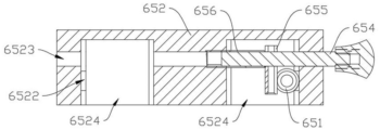
Further, referring to fig. 18 to 21, the third support table mechanism 620 includes a third support table 640 and a support assembly 650. The third supporting platform 640 may specifically adopt a vacuum absorption manner to fix the wafer 710, and the third supporting platform 640 includes a first supporting surface 641 for supporting the wafer 710, and a plurality of vacuum absorption holes (not shown) are uniformly distributed on the first supporting surface 641. The support assembly 650 is disposed at an outer edge of the third support table 640 to support the tool 720. The support assembly 650 can be extended or retracted along the radial direction of the third support stage 640, so as to improve the adaptability of the wafers 710 with different sizes, and avoid enlarging the third support stage 640, thereby reducing the cost.
The support assembly 650 includes a connecting rod 651, a support block 652, and a locking structure. The connecting rod 651 is fixed on the outer periphery of the third support table 640 along the radial direction of the third support table 640, the support block 652 is sleeved on the connecting rod 651 and can move along the axial direction of the connecting rod 651, the locking structure is arranged on the support block 652, the locking structure has a locking state for limiting the support block 652 to move along the axial direction of the connecting rod 651 and an unlocking state for releasing the limitation, the locking structure is suitable for being converted from the locking state to the unlocking state through pressing operation, and when the pressing force is removed, the unlocking state is reset to the locking state.
The support block 652 has a second support surface 6521 substantially flush with the first support surface 641, and the second support surface 6521 is used for supporting the tool 720. Preferably, in order to improve the reliability of the fixture 720 on the supporting block 652, the supporting block 652 and the fixture 720 are magnetically matched. The tool 720 may be made of a magnetic conductive material, and the supporting block 652 is provided with a magnetic member 653, and the magnetic member 653 abuts against the second supporting surface 6521. In this embodiment, the supporting members 650 are provided in a plurality and uniformly distributed along the circumferential direction of the third supporting platform 640, so as to effectively support different areas on the circumferential side of the fixture 720.
The locking structure includes a movable bar 654, a locking block 655, and a resilient member 656. The movable rod 654 is movably connected with the supporting block 652, the locking block 655 is fixedly connected with the movable rod 654, and the resilient member 656 is a spring, which is disposed on the locking block 655 and provides a resilient force for restoring the movable rod 654 from the unlocked state to the locked state, when the movable rod 654 is in the unlocked state, the locking block 655 is away from the connecting rod 651, and when the movable rod 654 is in the locked state, the locking block 655 is abutted against the connecting rod 651 to limit the movement of the supporting block 652.
Specifically, the supporting block 652 is provided with a first connecting hole 6522 and a second connecting hole 6523, the supporting block 652 is movably sleeved on the connecting rod 651 through the first connecting hole 6522, and the movable rod 654 is movably inserted into the second connecting hole 6523 and intersects with the connecting rod 651.
The supporting block 652 further defines a receiving cavity 6524 respectively communicating with the first connecting hole 6522 and the second connecting hole 6523, and the connecting rod 651 and the movable rod 654 are partially located in the receiving cavity 6524. The locking block 655 is fixed on the portion of the movable rod 654 in the receiving cavity 6524, and the resilient member 656 is limitedly disposed in the receiving cavity 6524 in the axial direction of the movable rod 654 to abut the locking block 655 on the portion of the connecting rod 651 in the receiving cavity 6524, thereby ensuring that the supporting block 652 is fastened on the first connecting hole 6522.
Preferably, the receiving cavity 6524 is recessed inwardly from a surface of the support block 652 opposite to the second support surface 6521, and the locking block 655 and the resilient member 656 may be received in the receiving cavity 6524 from an open side of the receiving cavity 6524. Since the locking block 655 is located in the receiving cavity 6524, it is restrained by the inner wall of the receiving cavity 6524 and the connecting rod 651 in the axial direction of the movable rod 654, thereby preventing the movable rod 654 from being separated from the support block 652. Because it is equipped with open side to accept the chamber 6524, and set up with second holding surface 6521 is relative, the locking structure of easy to assemble, and avoid piece or dust to get into in the course of working and receive the chamber 6524, improve the reliability of locking structure.
Preferably, in order to improve the supporting reliability of the supporting block 652, the supporting block 652 is provided with connecting rods 651 on both sides thereof, and correspondingly, the locking structures correspond to the connecting rods 651 one to respectively abut against the two movable rods 654.
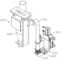
Further, referring to fig. 22 and 23, the laser mechanism 630 includes a third lifting assembly 631 and a laser 632 disposed on the third lifting assembly 631, the third lifting assembly 631 can drive the laser 632 to approach or depart from the wafer 710 along the Z-axis direction, a displacement sensor (not shown) for measuring the surface height of the wafer 710 is disposed on the third lifting assembly 631, and the sensor specifically adopts a non-contact displacement sensor, preferably a laser displacement sensor. Because the surface of the wafer 710 is not absolutely flat, the difference in height between the surfaces of the wafer 710 may cause the actual laser cutting position to deviate, the surface height of the wafer 710 is measured by the displacement sensor, and the third lifting assembly 631 can adaptively adjust the height of the laser 632 according to the measurement result, thereby dynamically compensating for the laser focus height. Specifically, the third lifting assembly 631 is lifted by a motor controlled screw, the displacement sensor detects the surface height of the wafer 710 in real time, and introduces the measured value into a motion controller (not shown) of the laser mechanism 630, the motion controller converts the received measured value data into a digital quantity, and then transmits the digital quantity to the motor of the third lifting assembly 631, and the motor moves the corresponding amount in real time according to the digital quantity, thereby solving the difficulty of consistency of the laser focus height. In order to improve the lifting precision, the motor is preferably a piezoelectric ceramic motor with nanometer resolution.
Preferably, the laser mechanism 630 further includes a dust suction assembly 633, and the dust suction assembly 633 is used for absorbing the debris generated during the grooving process of the wafer 710, so as to improve the smoothness of the grooving apparatus 600.
The dust suction assembly 633 comprises a dust suction main body 634 for providing suction force and a dust suction head 635 communicated with the dust suction main body 634, wherein the dust suction head 635 is arranged at a laser emitting part 6321 of the laser 632, so that the dust suction effect is improved by being close to a grooved area of the wafer 710.
Specifically, the dust collection head 635 is located right below the laser emission portion 6321, a dust collection cavity 6351 communicated with the dust collection host 634 is formed in the dust collection head 635, the dust collection head 635 has a top wall facing the laser emission portion 6321 and a bottom wall facing the wafer 710, the top wall and the bottom wall of the dust collection head 635 are respectively provided with a third opening 6352 and a fourth opening 6353 communicated with the dust collection cavity 6351 along the Z-axis direction, the laser emission portion 6321, the third opening 6352 and the fourth opening 6353 are coaxially arranged, light emitted from the laser emission portion 6321 can sequentially emit to the wafer 710 through the third opening 6352, the dust collection cavity 6351 and the fourth opening 6353, and debris generated by the groove opening of the wafer 710 can be sucked into the dust collection cavity 6351 through the fourth opening 6353 and finally flows into the dust collection host 634. Preferably, for convenience of mounting the dust suction head 635 on the laser emitting portion 6321, in this embodiment, the dust suction head 635 is in plug-in fit with the laser emitting portion 6321.
Since the laser 632 will move up and down along the Z-axis direction during the actual grooving process, in order to avoid the dust suction assembly 633 limiting the movement of the laser 632, in this embodiment, the dust suction assembly 633 further includes a dust suction duct 636 connected between the dust suction main unit 634 and the dust suction head 635, and the dust suction duct 636 is at least partially retractable along the Z-axis direction to drive the dust suction head 635 to move synchronously along the Z-axis direction along with the laser 632. Specifically, the dust suction duct 636 may be at least partially a non-rigid tube such as a hose or a bellows, so as to avoid the rigid connection of the dust suction head 635 with the dust suction main unit 634 in the Z-axis direction.
In addition, the invention also provides a grooving method, which comprises the following steps:
s1: the first carrying device 200 moves to the pick-and-place position of the loading device 100 to take out the wafer assembly 700 to be grooved, and moves the wafer assembly 700 to the buffer station;
s2: the cleaning device 300 receives the wafer assembly 700 at the cache station for cleaning and returns the wafer assembly 700 to the cache station after the cleaning is finished;
s3: the first transfer device 200 continues to move the wafer assembly 700 to the coating station of the coating device 400, and the coating device 400 receives the wafer assembly 700 to coat the wafer assembly with the protective liquid and returns the wafer assembly to the coating station after coating is completed;
s4: the first carrying device 200 moves the wafer assembly 700 back to the buffer station, the first carrying mechanism 510 of the second carrying device 500 moves the wafer assembly 700 to the slotting device 600 for slotting, and meanwhile, the second carrying mechanism 520 of the second carrying device 500 moves the wafer assembly 700 after slotting on the slotting device 600 back to the buffer station;
s5: the cleaning device 300 receives the wafer assembly 700 after the buffer station has finished slotting and performs cleaning again, and the first carrying device 200 moves the slotted and cleaned wafer assembly 700 back to the loading device 100, and repeats the above operations, so as to realize continuous processing of the wafer assembly 700.
Preferably, when the wafer assembly 700 is transferred between the buffer station and the loading device 100, the wafer assembly 700 is clamped by the first transfer device 200 toward the clamp 223 of the loading device 100; when the wafer assembly 700 is transferred between the buffer station and the coating station, the wafer assembly 700 is held by the first transfer device 200 facing away from the holder 223 of the loading device 100.
Preferably, in the slotting process of the slotting device 600, the slotting device 600 firstly slots a slot on each of two sides of the cutting track, the slot is a narrow line slot, and the step determines the risk of laser slotting and cracking; then, at least one groove is formed between two narrow grooves, which are wide grooves, and the laser grooving depth is determined to finally complete the cutting groove of the wafer 710.
In addition, the present invention also provides a full-dicing system for dividing the whole wafer 710 into single dies for packaging into chips, which has an important impact on the yield of chip manufacture and the production cost. The full-cutting system comprises the automatic slotting equipment and the wafer laser concealed cutting equipment (not shown). During working, firstly, automatic slotting equipment is used for removing media in a cutting track area on the front surface of the wafer 710 to form a groove shape (preferably a uniform U-shaped groove) with uniform depth and adjustable width; then, a semi-transparent long laser beam is focused inside the wafer 710 from the back surface of the wafer 710 by using a wafer laser stealth cutting device to form a segmentation starting point, so that the structural strength of the wafer 710 is reduced, the wafer 710 is segmented from the inside under the action of external force, and the wafer 710 is not broken and has constant stability. Preferably, to complete the dicing of the wafer 710, the full-cutting system further includes a wafer breaking apparatus (not shown) for mechanically or laser breaking the undercut wafer 710 to separate the undercut wafer into a plurality of chip particles with predetermined sizes.
The above description is only for the purpose of illustrating embodiments of the present invention and is not intended to limit the scope of the present invention, and all modifications, equivalents, and equivalent structures or equivalent processes that can be used directly or indirectly in other related fields of technology shall be encompassed by the present invention.
Claims (16)
1. An automatic grooving apparatus, comprising:
a loading device (100) for storing the wafer assembly (700);
a cleaning device (300) for cleaning the wafer assembly (700);
a coating device (400) for coating the wafer assembly (700);
a first transfer device (200) capable of transferring wafer assemblies (700) to and from the loading device (100), the cleaning device (300) and the coating device (400), wherein the first transfer device (200) is provided with a buffer station;
the slotting device (600) is used for slotting the wafer assembly (700);
a second handling device (500) for handling wafer assemblies (700) back and forth between the buffer station and the slotting device (600);
wherein the second conveying device (500) comprises a first conveying mechanism (510) and a second conveying mechanism (520), and the moving directions of the first conveying mechanism (510) and the second conveying mechanism (520) are opposite.
2. The automatic slotting device as claimed in claim 1, wherein said feeding device (100) comprises a placing table (120) for placing a wafer box, said placing table (120) comprising:
a storage bin (121) provided with a pick-and-place inlet (122) at one side facing the first carrying device (200), and a pick-and-place outlet (123) at the side opposite to the pick-and-place inlet (122);
the placing plate (140) is connected in the containing bin (121) in a sliding mode and can be pulled out of the containing bin (121) through the placing outlet (123).
3. The automatic slotting device as claimed in claim 2, wherein the storage bin (121) is provided with a first abutting member (125) and a second abutting member (126) at two sides of the placing plate (140) in the sliding direction, the placing plate (140) is provided with a third abutting member (141) limited between the first abutting member (125) and the second abutting member (126), the third abutting member (141) is in magnetic attraction fit with the first abutting member (125), and the third abutting member (141) is in magnetic attraction fit with the second abutting member (126).
4. The automated grooving apparatus according to claim 2, wherein the loading device (100), the cleaning device (300), and the coating device (400) are arranged along an X-axis direction, the first handling device (200) includes a gripping mechanism (220) that can shuttle among the loading device (100), the cleaning device (300), and the coating device (400) along the X-axis direction and pick and place the wafer assembly (700), the loading device (100) includes a lifting mechanism (110) drivingly connected to the placing table (120), and the lifting mechanism (110) is adapted to drive the placing table (120) to lift along a Z-axis direction.
5. The automated slotting machine as claimed in claim 4, wherein the first handling device (200) comprises a first carrying mechanism (230) having the buffer station, the first carrying mechanism (230) is suitable for positioning the position of the wafer assembly (700) in the Y-axis direction, and the grabbing mechanism (220), the first carrying mechanism (230) and the cleaning device (300) are arranged in sequence from top to bottom.
6. The automatic slotting device as claimed in claim 4, wherein the grabbing mechanism (220) comprises two clamping members (223) for taking and placing the wafer assembly (700), one clamping member (223) faces the taking and placing inlet (122) of the loading device (100), and the other clamping member (223) faces away from the taking and placing inlet (122) of the loading device (100).
7. The automated slotting device as recited in claim 1, wherein the cleaning device (300) comprises:
a first shell (310) which is internally provided with a cleaning cavity (311), wherein the top of the cleaning cavity (311) is provided with a first opening (312);
the first supporting platform mechanism (320) comprises a first lifting component (321), a first rotating component (322) arranged on the first lifting component (321) and a first supporting platform (323) arranged on the first rotating component (322) and contained in the cleaning cavity (311), and the first supporting platform (323) can extend out through the first opening (312);
a first spray head mechanism (330) located within the wash chamber (311) and comprising a wash spray head (332) facing the first support stage (323);
the side wall of the cleaning cavity (311) is provided with a first splash-proof structure (340) for blocking cleaning liquid from flowing out of the first opening (312), and/or the first opening (312) is provided with a cover structure (350), and the cover structure (350) can open or close the first opening (312).
8. The automatic grooving apparatus of claim 1, wherein the coating device (400) comprises:
a second housing (430) in which a coating chamber (431) is formed, the top of the coating chamber (431) being opened with a second opening (432);
a second supporting table mechanism (420) including a second rotating assembly (421) and a second supporting table (422) disposed on the second rotating assembly (421) and accommodated in the coating chamber (431), the second supporting table (422) being capable of protruding through the second opening (432);
the second bearing mechanism (410) is positioned above the second shell (430), is suitable for positioning the position of the wafer assembly (700) in the Y-axis direction and can lift along the Z-axis direction;
the second housing (430) is of a liftable structure, and the second housing (430) has a descending state for driving the second supporting platform (422) to be exposed from the second opening (432) and an ascending state for driving the second supporting platform (422) to be in the coating cavity (431).
9. The automated slotting device according to claim 8, wherein a second splash guard structure (450) is provided above the second carrier mechanism (410), the second splash guard structure (450) covering the second opening (432) when the second housing (430) is in the raised state.
10. The automated slotting machine of claim 1, wherein the first handling mechanism (510) and the second handling mechanism (520) are identical in structure, the first handling mechanism (510) comprising:
a second linear module (511);
the second mounting frame (512) comprises a mounting frame main body (5121) in transmission connection with the second linear module (511) and at least two movable plates (5122) movably connected to the mounting frame main body (5121);
a plurality of pick-and-place devices (513) for picking and placing the wafer assembly (700) and respectively fixed on the two movable plates (5122);
the dustproof structure (514) is positioned above the picking and placing part (513) and can cover the wafer assembly (700) at the picking and placing part (513);
wherein the movable plate (5122) is movably adjustable relative to the mounting frame body (5121) along a radial direction of the wafer assembly (700).
11. The automated slotting device of claim 1, wherein the slotting device (600) comprises:
a translation mechanism (610) movable along X-axis and Y-axis directions;
the third support table mechanism (620) is in transmission connection with the translation mechanism (610);
the laser mechanism (630) is arranged above the third supporting table mechanism (620) and is positioned in the moving stroke range of the translation mechanism (610), and the laser mechanism (630) comprises a laser (632), a third lifting assembly (631) and a dust suction assembly (633), wherein the third lifting assembly (631) drives the laser (632) to lift along the Z-axis direction;
the dust collection assembly (633) comprises a dust collection main machine (634) used for providing suction force and a dust collection head (635) communicated with the dust collection main machine (634), wherein the dust collection head (635) is arranged at a laser emitting part (6321) of the laser (632) and can synchronously lift along with the laser (632).
12. The automated slotting apparatus according to claim 11, wherein the third support table mechanism (620) includes:
a third support stage (640) for supporting a wafer (710) of the wafer assembly (700);
the supporting assembly (650) is arranged at the outer edge of the third supporting table (640) and is used for supporting the tool (720) of the wafer assembly (700);
wherein the support assembly (650) is expandable or contractible in a radial direction of the third support table (640).
13. The automated slotting apparatus of claim 12, where the support assembly (650) comprises:
a connecting rod (651) fixed to the outer periphery of the third support table (640) in the radial direction of the third support table (640);
the supporting block (652) is sleeved on the connecting rod (651) and can move along the axial direction of the connecting rod (651);
a locking structure provided on the support block (652) and having a locked state restricting the support block (652) from moving in the axial direction of the connecting rod (651) and an unlocked state restricting unlocking, the locking structure being shifted from the locked state to the unlocked state in response to a pressing operation and being adapted to be reset from the unlocked state to the locked state when the pressing is released.
14. A grooving method including the automatic grooving apparatus of any one of claims 1 to 13, comprising the steps of:
s1: the first carrying device (200) moves to the pick-and-place position of the loading device (100) to take out the wafer assembly (700) to be grooved, and the wafer assembly (700) is moved to a buffer station;
s2: the cleaning device (300) receives the wafer assembly (700) at the caching station for cleaning, and returns the wafer assembly to the caching station after cleaning;
s3: the first carrying device (200) continuously moves the wafer assembly (700) to a coating station of the coating device (400), and the coating device (400) receives the wafer assembly (700) to coat the wafer assembly with the protective liquid and returns the wafer assembly to the coating station after coating is finished;
s4: the first carrying device (200) moves the wafer assembly (700) back to the buffer station, the first carrying mechanism (510) of the second carrying device (500) moves the wafer assembly (700) to the slotting device (600) for slotting, and meanwhile, the second carrying mechanism (520) of the second carrying device (500) moves the wafer assembly (700) after slotting on the slotting device (600) back to the buffer station;
s5: the cleaning device (300) receives the wafer assembly (700) subjected to slotting in the buffer station and cleans the wafer assembly again, and the first carrying device (200) moves the wafer assembly (700) subjected to slotting and cleaning back to the loading device (100).
15. The grooving method according to claim 14, wherein when transferring the wafer assembly (700) between the buffer station and the loading device (100), the wafer assembly (700) is held by the first handling device (200) toward the holding member (223) of the loading device (100); when the wafer assembly (700) is transferred between the buffer storage station and the coating station, the wafer assembly (700) is clamped by the first carrying device (200) in a way of being opposite to a clamping piece (223) of the loading device (100).
16. A full cutting system comprising an automated slotting device as claimed in any one of claims 1 to 13.
Priority Applications (1)
| Application Number | Priority Date | Filing Date | Title |
|---|---|---|---|
| CN202211690556.9A CN115662926B (en) | 2022-12-28 | 2022-12-28 | Automatic slotting equipment, slotting method and full-cutting system |
Applications Claiming Priority (1)
| Application Number | Priority Date | Filing Date | Title |
|---|---|---|---|
| CN202211690556.9A CN115662926B (en) | 2022-12-28 | 2022-12-28 | Automatic slotting equipment, slotting method and full-cutting system |
Publications (2)
| Publication Number | Publication Date |
|---|---|
| CN115662926A true CN115662926A (en) | 2023-01-31 |
| CN115662926B CN115662926B (en) | 2023-06-06 |
Family
ID=85022188
Family Applications (1)
| Application Number | Title | Priority Date | Filing Date |
|---|---|---|---|
| CN202211690556.9A Active CN115662926B (en) | 2022-12-28 | 2022-12-28 | Automatic slotting equipment, slotting method and full-cutting system |
Country Status (1)
| Country | Link |
|---|---|
| CN (1) | CN115662926B (en) |
Cited By (2)
| Publication number | Priority date | Publication date | Assignee | Title |
|---|---|---|---|---|
| CN116344423A (en) * | 2023-05-29 | 2023-06-27 | 上海新创达半导体设备技术有限公司 | Material handling crown block based on wireless power supply and control method thereof |
| CN117415479A (en) * | 2023-12-19 | 2024-01-19 | 苏州镭明激光科技有限公司 | Cutting device, cutting method and cutting system |
Citations (4)
| Publication number | Priority date | Publication date | Assignee | Title |
|---|---|---|---|---|
| CN207447554U (en) * | 2017-08-15 | 2018-06-05 | 深圳市集银科技有限公司 | The automatic press welders of FPC |
| CN214815772U (en) * | 2020-12-30 | 2021-11-23 | 大族激光科技产业集团股份有限公司 | Wafer laser processing device |
| CN114918562A (en) * | 2022-05-31 | 2022-08-19 | 深圳华工新能源装备有限公司 | Wafer cutting machine and cutting method |
| CN217989849U (en) * | 2022-08-30 | 2022-12-09 | 厦门竣铭科技有限公司 | Blue membrane point gum machine |
-
2022
- 2022-12-28 CN CN202211690556.9A patent/CN115662926B/en active Active
Patent Citations (4)
| Publication number | Priority date | Publication date | Assignee | Title |
|---|---|---|---|---|
| CN207447554U (en) * | 2017-08-15 | 2018-06-05 | 深圳市集银科技有限公司 | The automatic press welders of FPC |
| CN214815772U (en) * | 2020-12-30 | 2021-11-23 | 大族激光科技产业集团股份有限公司 | Wafer laser processing device |
| CN114918562A (en) * | 2022-05-31 | 2022-08-19 | 深圳华工新能源装备有限公司 | Wafer cutting machine and cutting method |
| CN217989849U (en) * | 2022-08-30 | 2022-12-09 | 厦门竣铭科技有限公司 | Blue membrane point gum machine |
Cited By (3)
| Publication number | Priority date | Publication date | Assignee | Title |
|---|---|---|---|---|
| CN116344423A (en) * | 2023-05-29 | 2023-06-27 | 上海新创达半导体设备技术有限公司 | Material handling crown block based on wireless power supply and control method thereof |
| CN116344423B (en) * | 2023-05-29 | 2023-08-11 | 上海新创达半导体设备技术有限公司 | Material handling crown block based on wireless power supply and control method thereof |
| CN117415479A (en) * | 2023-12-19 | 2024-01-19 | 苏州镭明激光科技有限公司 | Cutting device, cutting method and cutting system |
Also Published As
| Publication number | Publication date |
|---|---|
| CN115662926B (en) | 2023-06-06 |
Similar Documents
| Publication | Publication Date | Title |
|---|---|---|
| CN115662926A (en) | Automatic slotting equipment, slotting method and full-cutting system | |
| CN106956370B (en) | Conveying mechanism of processing device | |
| CN110696416B (en) | Graphite bipolar plate molding system | |
| CN105935793B (en) | Engraving and milling machine and control method thereof | |
| TWI699265B (en) | Cutting device | |
| KR20150044364A (en) | Strip grinder | |
| KR101635113B1 (en) | Semiconductor strip grinder | |
| KR101505891B1 (en) | Working apparatus, and cover for the working apparatus | |
| KR200480692Y1 (en) | Machining apparatus of plate | |
| CN211222178U (en) | Graphite bipolar plate compression molding system | |
| CN210231298U (en) | Automatic feeding and discharging machine for side feeding | |
| WO2016189682A1 (en) | Deposit removal method and deposit removal device | |
| KR102349650B1 (en) | System for automatic polishing | |
| CN212071388U (en) | Full-automatic edge scraping machine | |
| CN209831280U (en) | Wafer multistation edge polishing equipment | |
| CN116100745A (en) | Automatic blanking equipment for earphone injection molding parts | |
| TW202245982A (en) | Auxiliary device capable of automatically replacing cutting blades | |
| CN110416112B (en) | Cleaning device | |
| CN114160378A (en) | Dispensing equipment | |
| CN111408990B (en) | Full-automatic edge scraping machine | |
| JP4295469B2 (en) | Polishing method | |
| CN219254521U (en) | Laser processing equipment and laser processing system | |
| JP4153413B2 (en) | Punching machine | |
| CN112008702A (en) | Transfer robot | |
| JPH09246790A (en) | Device for loading electronic part |
Legal Events
| Date | Code | Title | Description |
|---|---|---|---|
| PB01 | Publication | ||
| PB01 | Publication | ||
| SE01 | Entry into force of request for substantive examination | ||
| SE01 | Entry into force of request for substantive examination | ||
| GR01 | Patent grant | ||
| GR01 | Patent grant |