CN108698222B - 衬底搬送机器人及衬底搬送装置 - Google Patents
衬底搬送机器人及衬底搬送装置 Download PDFInfo
- Publication number
- CN108698222B CN108698222B CN201780013321.7A CN201780013321A CN108698222B CN 108698222 B CN108698222 B CN 108698222B CN 201780013321 A CN201780013321 A CN 201780013321A CN 108698222 B CN108698222 B CN 108698222B
- Authority
- CN
- China
- Prior art keywords
- guide rail
- cover
- robot
- substrate transfer
- substrate
- Prior art date
- Legal status (The legal status is an assumption and is not a legal conclusion. Google has not performed a legal analysis and makes no representation as to the accuracy of the status listed.)
- Active
Links
Images


Classifications
-
- H—ELECTRICITY
- H01—ELECTRIC ELEMENTS
- H01L—SEMICONDUCTOR DEVICES NOT COVERED BY CLASS H10
- H01L21/00—Processes or apparatus adapted for the manufacture or treatment of semiconductor or solid state devices or of parts thereof
- H01L21/67—Apparatus specially adapted for handling semiconductor or electric solid state devices during manufacture or treatment thereof; Apparatus specially adapted for handling wafers during manufacture or treatment of semiconductor or electric solid state devices or components ; Apparatus not specifically provided for elsewhere
- H01L21/677—Apparatus specially adapted for handling semiconductor or electric solid state devices during manufacture or treatment thereof; Apparatus specially adapted for handling wafers during manufacture or treatment of semiconductor or electric solid state devices or components ; Apparatus not specifically provided for elsewhere for conveying, e.g. between different workstations
- H01L21/67763—Apparatus specially adapted for handling semiconductor or electric solid state devices during manufacture or treatment thereof; Apparatus specially adapted for handling wafers during manufacture or treatment of semiconductor or electric solid state devices or components ; Apparatus not specifically provided for elsewhere for conveying, e.g. between different workstations the wafers being stored in a carrier, involving loading and unloading
- H01L21/67766—Mechanical parts of transfer devices
-
- B—PERFORMING OPERATIONS; TRANSPORTING
- B25—HAND TOOLS; PORTABLE POWER-DRIVEN TOOLS; MANIPULATORS
- B25J—MANIPULATORS; CHAMBERS PROVIDED WITH MANIPULATION DEVICES
- B25J11/00—Manipulators not otherwise provided for
- B25J11/0095—Manipulators transporting wafers
-
- B—PERFORMING OPERATIONS; TRANSPORTING
- B25—HAND TOOLS; PORTABLE POWER-DRIVEN TOOLS; MANIPULATORS
- B25J—MANIPULATORS; CHAMBERS PROVIDED WITH MANIPULATION DEVICES
- B25J18/00—Arms
- B25J18/02—Arms extensible
- B25J18/04—Arms extensible rotatable
-
- B—PERFORMING OPERATIONS; TRANSPORTING
- B25—HAND TOOLS; PORTABLE POWER-DRIVEN TOOLS; MANIPULATORS
- B25J—MANIPULATORS; CHAMBERS PROVIDED WITH MANIPULATION DEVICES
- B25J9/00—Programme-controlled manipulators
- B25J9/02—Programme-controlled manipulators characterised by movement of the arms, e.g. cartesian coordinate type
- B25J9/04—Programme-controlled manipulators characterised by movement of the arms, e.g. cartesian coordinate type by rotating at least one arm, excluding the head movement itself, e.g. cylindrical coordinate type or polar coordinate type
- B25J9/041—Cylindrical coordinate type
- B25J9/042—Cylindrical coordinate type comprising an articulated arm
-
- B—PERFORMING OPERATIONS; TRANSPORTING
- B25—HAND TOOLS; PORTABLE POWER-DRIVEN TOOLS; MANIPULATORS
- B25J—MANIPULATORS; CHAMBERS PROVIDED WITH MANIPULATION DEVICES
- B25J9/00—Programme-controlled manipulators
- B25J9/06—Programme-controlled manipulators characterised by multi-articulated arms
-
- B—PERFORMING OPERATIONS; TRANSPORTING
- B65—CONVEYING; PACKING; STORING; HANDLING THIN OR FILAMENTARY MATERIAL
- B65G—TRANSPORT OR STORAGE DEVICES, e.g. CONVEYORS FOR LOADING OR TIPPING, SHOP CONVEYOR SYSTEMS OR PNEUMATIC TUBE CONVEYORS
- B65G47/00—Article or material-handling devices associated with conveyors; Methods employing such devices
- B65G47/74—Feeding, transfer, or discharging devices of particular kinds or types
- B65G47/90—Devices for picking-up and depositing articles or materials
- B65G47/902—Devices for picking-up and depositing articles or materials provided with drive systems incorporating rotary and rectilinear movements
-
- B—PERFORMING OPERATIONS; TRANSPORTING
- B65—CONVEYING; PACKING; STORING; HANDLING THIN OR FILAMENTARY MATERIAL
- B65G—TRANSPORT OR STORAGE DEVICES, e.g. CONVEYORS FOR LOADING OR TIPPING, SHOP CONVEYOR SYSTEMS OR PNEUMATIC TUBE CONVEYORS
- B65G49/00—Conveying systems characterised by their application for specified purposes not otherwise provided for
- B65G49/05—Conveying systems characterised by their application for specified purposes not otherwise provided for for fragile or damageable materials or articles
- B65G49/07—Conveying systems characterised by their application for specified purposes not otherwise provided for for fragile or damageable materials or articles for semiconductor wafers Not used, see H01L21/677
-
- H—ELECTRICITY
- H01—ELECTRIC ELEMENTS
- H01L—SEMICONDUCTOR DEVICES NOT COVERED BY CLASS H10
- H01L21/00—Processes or apparatus adapted for the manufacture or treatment of semiconductor or solid state devices or of parts thereof
- H01L21/67—Apparatus specially adapted for handling semiconductor or electric solid state devices during manufacture or treatment thereof; Apparatus specially adapted for handling wafers during manufacture or treatment of semiconductor or electric solid state devices or components ; Apparatus not specifically provided for elsewhere
- H01L21/677—Apparatus specially adapted for handling semiconductor or electric solid state devices during manufacture or treatment thereof; Apparatus specially adapted for handling wafers during manufacture or treatment of semiconductor or electric solid state devices or components ; Apparatus not specifically provided for elsewhere for conveying, e.g. between different workstations
- H01L21/67703—Apparatus specially adapted for handling semiconductor or electric solid state devices during manufacture or treatment thereof; Apparatus specially adapted for handling wafers during manufacture or treatment of semiconductor or electric solid state devices or components ; Apparatus not specifically provided for elsewhere for conveying, e.g. between different workstations between different workstations
- H01L21/67706—Mechanical details, e.g. roller, belt
-
- H—ELECTRICITY
- H01—ELECTRIC ELEMENTS
- H01L—SEMICONDUCTOR DEVICES NOT COVERED BY CLASS H10
- H01L21/00—Processes or apparatus adapted for the manufacture or treatment of semiconductor or solid state devices or of parts thereof
- H01L21/67—Apparatus specially adapted for handling semiconductor or electric solid state devices during manufacture or treatment thereof; Apparatus specially adapted for handling wafers during manufacture or treatment of semiconductor or electric solid state devices or components ; Apparatus not specifically provided for elsewhere
- H01L21/677—Apparatus specially adapted for handling semiconductor or electric solid state devices during manufacture or treatment thereof; Apparatus specially adapted for handling wafers during manufacture or treatment of semiconductor or electric solid state devices or components ; Apparatus not specifically provided for elsewhere for conveying, e.g. between different workstations
- H01L21/67703—Apparatus specially adapted for handling semiconductor or electric solid state devices during manufacture or treatment thereof; Apparatus specially adapted for handling wafers during manufacture or treatment of semiconductor or electric solid state devices or components ; Apparatus not specifically provided for elsewhere for conveying, e.g. between different workstations between different workstations
- H01L21/67712—Apparatus specially adapted for handling semiconductor or electric solid state devices during manufacture or treatment thereof; Apparatus specially adapted for handling wafers during manufacture or treatment of semiconductor or electric solid state devices or components ; Apparatus not specifically provided for elsewhere for conveying, e.g. between different workstations between different workstations the substrate being handled substantially vertically
-
- H—ELECTRICITY
- H01—ELECTRIC ELEMENTS
- H01L—SEMICONDUCTOR DEVICES NOT COVERED BY CLASS H10
- H01L21/00—Processes or apparatus adapted for the manufacture or treatment of semiconductor or solid state devices or of parts thereof
- H01L21/67—Apparatus specially adapted for handling semiconductor or electric solid state devices during manufacture or treatment thereof; Apparatus specially adapted for handling wafers during manufacture or treatment of semiconductor or electric solid state devices or components ; Apparatus not specifically provided for elsewhere
- H01L21/677—Apparatus specially adapted for handling semiconductor or electric solid state devices during manufacture or treatment thereof; Apparatus specially adapted for handling wafers during manufacture or treatment of semiconductor or electric solid state devices or components ; Apparatus not specifically provided for elsewhere for conveying, e.g. between different workstations
- H01L21/67739—Apparatus specially adapted for handling semiconductor or electric solid state devices during manufacture or treatment thereof; Apparatus specially adapted for handling wafers during manufacture or treatment of semiconductor or electric solid state devices or components ; Apparatus not specifically provided for elsewhere for conveying, e.g. between different workstations into and out of processing chamber
- H01L21/67742—Mechanical parts of transfer devices
-
- H—ELECTRICITY
- H01—ELECTRIC ELEMENTS
- H01L—SEMICONDUCTOR DEVICES NOT COVERED BY CLASS H10
- H01L21/00—Processes or apparatus adapted for the manufacture or treatment of semiconductor or solid state devices or of parts thereof
- H01L21/67—Apparatus specially adapted for handling semiconductor or electric solid state devices during manufacture or treatment thereof; Apparatus specially adapted for handling wafers during manufacture or treatment of semiconductor or electric solid state devices or components ; Apparatus not specifically provided for elsewhere
- H01L21/677—Apparatus specially adapted for handling semiconductor or electric solid state devices during manufacture or treatment thereof; Apparatus specially adapted for handling wafers during manufacture or treatment of semiconductor or electric solid state devices or components ; Apparatus not specifically provided for elsewhere for conveying, e.g. between different workstations
- H01L21/67739—Apparatus specially adapted for handling semiconductor or electric solid state devices during manufacture or treatment thereof; Apparatus specially adapted for handling wafers during manufacture or treatment of semiconductor or electric solid state devices or components ; Apparatus not specifically provided for elsewhere for conveying, e.g. between different workstations into and out of processing chamber
- H01L21/67751—Apparatus specially adapted for handling semiconductor or electric solid state devices during manufacture or treatment thereof; Apparatus specially adapted for handling wafers during manufacture or treatment of semiconductor or electric solid state devices or components ; Apparatus not specifically provided for elsewhere for conveying, e.g. between different workstations into and out of processing chamber vertical transfer of a single workpiece
-
- H—ELECTRICITY
- H01—ELECTRIC ELEMENTS
- H01L—SEMICONDUCTOR DEVICES NOT COVERED BY CLASS H10
- H01L21/00—Processes or apparatus adapted for the manufacture or treatment of semiconductor or solid state devices or of parts thereof
- H01L21/67—Apparatus specially adapted for handling semiconductor or electric solid state devices during manufacture or treatment thereof; Apparatus specially adapted for handling wafers during manufacture or treatment of semiconductor or electric solid state devices or components ; Apparatus not specifically provided for elsewhere
- H01L21/677—Apparatus specially adapted for handling semiconductor or electric solid state devices during manufacture or treatment thereof; Apparatus specially adapted for handling wafers during manufacture or treatment of semiconductor or electric solid state devices or components ; Apparatus not specifically provided for elsewhere for conveying, e.g. between different workstations
- H01L21/67763—Apparatus specially adapted for handling semiconductor or electric solid state devices during manufacture or treatment thereof; Apparatus specially adapted for handling wafers during manufacture or treatment of semiconductor or electric solid state devices or components ; Apparatus not specifically provided for elsewhere for conveying, e.g. between different workstations the wafers being stored in a carrier, involving loading and unloading
- H01L21/67778—Apparatus specially adapted for handling semiconductor or electric solid state devices during manufacture or treatment thereof; Apparatus specially adapted for handling wafers during manufacture or treatment of semiconductor or electric solid state devices or components ; Apparatus not specifically provided for elsewhere for conveying, e.g. between different workstations the wafers being stored in a carrier, involving loading and unloading involving loading and unloading of wafers
-
- H—ELECTRICITY
- H01—ELECTRIC ELEMENTS
- H01L—SEMICONDUCTOR DEVICES NOT COVERED BY CLASS H10
- H01L21/00—Processes or apparatus adapted for the manufacture or treatment of semiconductor or solid state devices or of parts thereof
- H01L21/67—Apparatus specially adapted for handling semiconductor or electric solid state devices during manufacture or treatment thereof; Apparatus specially adapted for handling wafers during manufacture or treatment of semiconductor or electric solid state devices or components ; Apparatus not specifically provided for elsewhere
- H01L21/677—Apparatus specially adapted for handling semiconductor or electric solid state devices during manufacture or treatment thereof; Apparatus specially adapted for handling wafers during manufacture or treatment of semiconductor or electric solid state devices or components ; Apparatus not specifically provided for elsewhere for conveying, e.g. between different workstations
- H01L21/67739—Apparatus specially adapted for handling semiconductor or electric solid state devices during manufacture or treatment thereof; Apparatus specially adapted for handling wafers during manufacture or treatment of semiconductor or electric solid state devices or components ; Apparatus not specifically provided for elsewhere for conveying, e.g. between different workstations into and out of processing chamber
- H01L21/67748—Apparatus specially adapted for handling semiconductor or electric solid state devices during manufacture or treatment thereof; Apparatus specially adapted for handling wafers during manufacture or treatment of semiconductor or electric solid state devices or components ; Apparatus not specifically provided for elsewhere for conveying, e.g. between different workstations into and out of processing chamber horizontal transfer of a single workpiece
-
- H—ELECTRICITY
- H01—ELECTRIC ELEMENTS
- H01L—SEMICONDUCTOR DEVICES NOT COVERED BY CLASS H10
- H01L21/00—Processes or apparatus adapted for the manufacture or treatment of semiconductor or solid state devices or of parts thereof
- H01L21/67—Apparatus specially adapted for handling semiconductor or electric solid state devices during manufacture or treatment thereof; Apparatus specially adapted for handling wafers during manufacture or treatment of semiconductor or electric solid state devices or components ; Apparatus not specifically provided for elsewhere
- H01L21/683—Apparatus specially adapted for handling semiconductor or electric solid state devices during manufacture or treatment thereof; Apparatus specially adapted for handling wafers during manufacture or treatment of semiconductor or electric solid state devices or components ; Apparatus not specifically provided for elsewhere for supporting or gripping
- H01L21/687—Apparatus specially adapted for handling semiconductor or electric solid state devices during manufacture or treatment thereof; Apparatus specially adapted for handling wafers during manufacture or treatment of semiconductor or electric solid state devices or components ; Apparatus not specifically provided for elsewhere for supporting or gripping using mechanical means, e.g. chucks, clamps or pinches
- H01L21/68707—Apparatus specially adapted for handling semiconductor or electric solid state devices during manufacture or treatment thereof; Apparatus specially adapted for handling wafers during manufacture or treatment of semiconductor or electric solid state devices or components ; Apparatus not specifically provided for elsewhere for supporting or gripping using mechanical means, e.g. chucks, clamps or pinches the wafers being placed on a robot blade, or gripped by a gripper for conveyance
Abstract
本发明的机器人具备:升降驱动机构(1),使具有保持衬底的末端执行器的机器人臂升降;及盖器件,覆盖升降驱动机构(1);升降驱动机构(1)具有:固定部(2),具有在上下方向上延伸的导轨(10);及升降部(3),沿着导轨(10)被升降驱动;机器人臂具有:基部连杆(4),连结在升降部(3);及连杆部件,连结在基部连杆(4);盖器件具有:固定侧盖(20),设置在固定部(2),供升降部(3)在其内部移动;及导轨用盖(19),设置在升降部(3),覆盖当升降部(3)下降时露出的导轨(10)的上部。本发明可提供一种不伴随机器人臂的刚性降低等不良情况而能够使衬底搬送装置小型化的衬底搬送机器人。
Description
技术领域
本发明涉及一种用来搬送半导体制造用的晶圆等衬底的衬底搬送机器人、及具备所述机器人的衬底搬送装置。
背景技术
作为使用衬底搬送机器人的装置的一例,关于半导体制造装置,在图1及图2中表示代表性的装置。半导体制造装置101具备:晶圆处理装置106,对半导体晶圆W进行处理;前开式晶圆盒(FOUP,Front Opening Unified Pod)102,作为收纳晶圆W的容器;及晶圆搬送装置(衬底搬送装置),用来在晶圆处理装置106与前开式晶圆盒102之间搬送晶圆W。
在前开式晶圆盒102中收纳处理前或处理后的晶圆W,在晶圆处理装置106中,进行热处理、杂质导入处理、薄膜形成处理、光刻处理、洗净处理及平坦化处理等工艺处理。
晶圆处理装置106具备:处理空间形成部112,形成处理空间111;处理装置主体(省略图示),配置在处理空间111的内部,对晶圆W进行处理;及处理空间调整装置(省略图示),调整充满处理空间111的环境气体。
晶圆搬送装置107具备:准备空间形成部117,形成准备空间116;衬底搬送机器人31,配置在准备空间116;对准器119,配置在准备空间116,且调整晶圆W的方向;及准备空间调整装置(省略图示),调整充满准备空间116的环境气体。
准备空间形成部117形成为长方体箱状,衬底搬送机器人31配置在准备空间116的长度方向的大致中央部。
衬底搬送机器人31从前开式晶圆盒内空间105取出晶圆W,或将晶圆W放入到前开式晶圆盒内空间105。另外,衬底搬送机器人31从处理空间111取出晶圆W,或将晶圆W放入到处理空间111。
另外,衬底搬送机器人31在从前开式晶圆盒102将晶圆W搬送到晶圆处理装置106时,暂时将从前开式晶圆盒102取出的晶圆W搬送到对准器119,使各晶圆W的方向相同后对晶圆处理装置106放入。
衬底搬送机器人31为SCARA(Selective Compliance Assembly Robot Arm,选择顺应性装配机器手臂)型的水平多关节机器人,且具备:机器人臂62;基台63,供连结机器人臂62的基端部;及机器人手部(末端执行器)64,连结机器人臂62的前端部,且握持晶圆W。机器人臂62具有第1及第2连杆65、66。
另外,为了用来取出在前开式晶圆盒102内上下呈多层收纳的晶圆W并放入到晶圆处理装置106而进行的上下方向的移动,基台63具有:固定部46,固定在设置面45;及升降部47,设置成能够相对于固定部46在上下方向上移位(参照图2)。在升降部47,可回转地设置着机器人臂62的基端部。升降部47形成为圆筒状,且以它的轴线在上下方向上延伸的方式设置。升降部47的上部成为基台63的上部。通过对升降部47进行升降驱动,设置在机器人臂62的前端部的机器人手部64的位置上下变化。
包含基台63的衬底搬送机器人31由于配设在洁净环境也就是准备空间116内,所以为了防止因升降部47升降时产生的粉尘等引起升降部准备空间116内的污染,固定部46或升降部47被收纳到壳体67内,在贯通壳体67的顶板部的升降部47的延伸部设置着机器人臂62。
在所述晶圆搬送装置107中,为了容易维持洁净环境等,较理想的是准备空间的大小、也就是准备空间形成部117的容积尽可能小。
例如,在专利文献1中,为了减小准备空间的深度方向(与前开式晶圆盒的排列方向正交的方向)的尺寸,而将衬底搬送机器人31靠近准备空间的深度方向的一侧配置,由此,减小将机器人臂收缩时到臂前端的长度。
然而,在该情况下,仍然无法将准备空间的深度方向的尺寸设为比构成机器人臂的各连杆的长度更小的尺寸。
这样,对于晶圆搬送装置107中所使用的衬底搬送机器人31存在以下背道而驰的要求:将水平面内的最大到达距离维持为指定大小,另一方面,尽可能缩短将机器人臂收缩时到臂前端的长度。
对于此种要求,由于可能产生新的污染源的移行轴(使机器人在前开式晶圆盒的排列方向上移行的轴)的配设并不优选,所以考虑通过增加构成机器人臂的连杆的根数并且缩短各连杆的长度来解决。
然而,为了防止衬底搬送机器人动作时的振动,必须充分确保构成机器人臂的各连杆的刚性,如果为了充分确保刚性而维持各连杆上下方向的高度(厚度)并且使连杆的个数增加,那么与连杆个数的增加相应地,机器人臂整体的上下方向的高度(厚度)会增加,从而握持晶圆的手部的最低高度变得比以往高。由此,存在手部无法拿到收纳在前开式晶圆盒内最下方位置的晶圆的问题。
背景技术文献
专利文献
专利文献1:日本专利第4980127号公报
发明内容
[发明要解决的问题]
本发明是鉴于所述以往技术的问题点而完成的,提供一种不伴随机器人臂的刚性降低等不良情况而能够使衬底搬送装置小型化的衬底搬送机器人、及具备所述机器人的衬底搬送装置。
[解决问题的技术手段]
为了解决所述问题,本发明的第1形态的衬底搬送机器人的特征在于具备:机器人臂,在前端部具有用来保持衬底的末端执行器;升降驱动机构,用来使所述机器人臂升降;及盖器件,用来覆盖所述升降驱动机构;且所述升降驱动机构具有:固定部,设置着在上下方向上延伸的导轨;及升降部,沿着所述导轨被升降驱动;所述机器人臂具有:基部连杆,可回转地连结在所述升降部;及连杆部件,可回转地连结在所述基部连杆,且包含所述前端部;所述盖器件具有:固定侧盖,设置在所述固定部,供所述升降部在其内部移动;及导轨用盖,设置在所述升降部,用来覆盖当所述升降部下降时露出的所述导轨的上部。
本发明的第2形态是根据第1形态,其特征在于:构成为当所述升降部下降到最低点时,所述基部连杆的上表面高度大致等于或低于所述固定部的上表面高度。
本发明的第3形态是根据第1或第2形态,其特征在于:构成为当所述升降部下降到最低点时,所述导轨用盖的上端与所述固定部的上表面高度大致相同。
本发明的第4形态是根据第1至第3中任一形态,其特征在于:所述连杆部件具有相互可回转地连结的2个以上的连杆。
为了解决所述问题,本发明的第5形态的衬底搬送装置的特征在于具备:第1至第4中任一形态的衬底搬送机器人;以及准备空间形成部,在内部设置着所述衬底搬送机器人。
本发明的第6形态是根据第5形态,其特征在于:所述衬底搬送机器人具有包含所述升降驱动机构的基台,所述基台靠近所述准备空间形成部的内部的深度方向的一侧配置。
[发明效果]
根据本发明,可提供一种不伴随机器人臂的刚性降低等不良情况而能够使衬底搬送装置小型化的衬底搬送机器人。
附图说明
图1是表示半导体制造装置的一例的俯视图。
图2是图1所示的半导体制造装置的纵剖视图。
图3是表示在本发明的一实施方式的衬底搬送机器人中,使升降部下降到最低点的状态的固定部及升降部的构造的剖视图。
图4是图3的A-A剖视图。
图5是图3的X-X剖视图。
图6是表示在图3所示的衬底搬送机器人中,使升降部上升到最高点的状态的固定部及升降部的构造的剖视图。
图7是图6的Y-Y剖视图。
图8是表示在图3所示的衬底搬送机器人中,使升降部下降到最低点的状态的固定部及升降部的外形图。
图9是图8的右侧视图。
图10是图8的俯视图。
图11是表示在图3所示的衬底搬送机器人中,使升降部上升到最高点的状态的固定部及升降部的外形图。
图12是图11的右侧视图。
图13是表示具备图3所示的衬底搬送机器人的衬底搬送装置的俯视图。
具体实施方式
以下,一边参照附图一边对本发明的一实施方式的衬底搬送机器人进行说明。
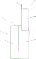
如图3至图5所示,本实施方式的衬底搬送机器人具备用来使机器人臂升降的升降驱动机构1,该升降驱动机构1具有:固定部2,固定在设置面;及升降部3,可升降地设置在固定部2的侧部。在升降部3的上部,可水平回转地设置着机器人臂的基部连杆4。在机器人臂的前端部,设置着用来保持衬底的手部(末端执行器)(省略图示)。
升降驱动机构1的固定部2具备外形呈纵向较长的大致长方体形状的固定侧外壳5(参照图3、图4、图8至图10)。在固定侧外壳5的内部配设着:滚珠丝杠6,用来使升降部3升降;螺母部件7,与滚珠丝杠6卡合,通过滚珠丝杠6的旋转而升降;电动机8,旋转驱动滚珠丝杠6;以及作为动力传递机构的滑轮机构9,用来将电动机8的驱动力传递给滚珠丝杠6。
另外,在固定部2的连结升降部3的侧面的外表面,设置指定间隔而平行地配设着2条在上下方向上延伸的导轨10。进而,在固定侧外壳5的内部下部,配设着用来将内部的空气从下方朝外部排出而使内部产生朝下的气流的风扇11。
升降部3具备可动侧外壳12(参照图3、4),该可动侧外壳12的外形呈纵向较长的大致长方体形状,且底部开放,顶板面及4个侧面以板状部件连结。在可动侧外壳12的与固定部2的连结侧的面,配设着:支撑部件13,连结在固定部2的固定侧外壳5内的螺母部件7;以及块状的移动体14,与导轨10卡合并上下升降。此外,为了确保移行的稳定性、确实性,移动体14在导轨10分别串联地配设着2个。
支撑部件13由于贯通与升降部3连结一侧的固定侧外壳5的侧面壁,所以在固定侧外壳5的所述侧面壁,设置着与升降部3的升降行程对应的长度的纵向细长的开口15,以使支撑部件13能够升降(参照图3、4)。
在升降部3的可动侧外壳12的上表面,可回转地设置着机器人臂的基部连杆4,在可动侧外壳12的内部配设着线缆配置区域16,该线缆配置区域16引绕着针对配设在基部连杆4及它的前端的连杆部件(包含1个或2个以上的连杆)内部的伺服电动机等的供电线缆或信号线缆。另外,在可动侧外壳12内,为了在升降部3升降时处理这些线缆类,而配设着线缆拖链(Cableveyor)(注册商标)17。
本实施方式中,在机器人臂位于最下方位置的情况下,如图3所示,以基部连杆4的上表面成为与固定侧外壳5的上表面大致相同的高度的方式,设定可动侧外壳12的上表面高度。
因此,如图13所示,通过将具有使以往的衬底搬送装置中所使用的2个连杆短条化而成的第1连杆65A及第2连杆66A的水平回转型臂机构用作连结在基部连杆4的连杆部件而构成机器人臂62A,可在不使各连杆的刚性降低的情况下将臂部前端的手部的高度位置维持为与以往相同。
其结果为,在本实施方式的衬底搬送机器人中,可在不使各连杆的刚性降低的情况下包括基部连杆4在内将连杆的根数设为3根,且可在实现与以往2根连杆的衬底搬送机器人相同的手部最大到达距离的基础上缩短各连杆的长度。
而且,如图13所示,将衬底搬送机器人的基台63靠近准备空间形成部116内部的深度方向的一侧配置,由此,由于晶圆搬送装置的准备空间116的深度方向的尺寸依赖于衬底搬送机器人的各连杆的长度而设定,所以伴随着各连杆的长度变短,可减小准备空间的宽度。也就是说,根据本实施方式的衬底搬送机器人,通过使各连杆的长度比以往短,可一边确保指定的手部最大到达距离,一边使准备空间的宽度减少。
另外,在如上所述的本实施方式中,在机器人臂位于最下方位置的情况下,可动侧外壳12的上表面高度以基部连杆4的上表面成为与固定侧外壳5的上表面大致相同的高度的方式设定。
因此,可动侧外壳12的上表面成为比固定侧外壳5的上表面低大致相当于基部连杆4的高度(厚度)的位置,其结果为,当使升降部3下降到最低点时,导轨10的上部露出。如果导轨10的上部露出,那么有可能因来自此处的粉尘等导致准备空间受到污染,所以需要采取一些对策。
因此,在本实施方式中,通过采用下述构成,来谋求防止以导轨10为污染源的污染。
也就是说,将用来覆盖升降部3下降时露出的导轨10的上部的导轨用盖19设置在升降部3的上部。具体来说,导轨用盖19形成为可动侧外壳12的与固定部2的连结面的上方延长部。可动侧外壳12及导轨用盖19构成用来覆盖升降驱动机构1的盖器件的一部分。
导轨用盖19的宽度与可动侧外壳12的与固定部2的连结面大致相同,高度以在升降部3下降到最低点的位置时覆盖露出的导轨10的上部表面的方式设定。
此外,为了防止来自导轨10的粉尘等流入到准备空间,而使导轨10与下文所述的顶板部盖21的间隙极小化,为此,导轨用盖19优选设为与固定侧外壳5的上表面高度大致相同。
另外,在固定侧外壳5具备固定侧盖20,该固定侧盖20具有与可动侧外壳12中除了与固定侧外壳5连结的侧部以外的侧部的外表面接近的侧面及底面,且上部开放。固定侧外壳5及固定侧盖20构成用来覆盖升降驱动机构1的盖器件的一部分。
构成升降部3的可动侧外壳12经过固定侧盖20的开放上部而升降,由此可出入于固定侧盖20的内部,且当可动侧外壳12位于下降到最低点的位置时,能够将可动侧外壳12的比大致上端部的高度靠下方的部分整体或一部分收容到固定侧盖20的内部。
通过使固定侧盖20的侧部内表面成为接近于可动侧外壳12的侧部外表面的形状,可抑制固定侧盖20内部的粉尘等经由固定侧盖20的侧部内表面与可动侧外壳12的侧部外表面的间隙向外部释出。
此外,在固定侧盖20设置底面的原因在于:当可动侧外壳12上升时,固定侧盖20的内部会与导轨10存在的空间连通(例如参照图6),所以通过将固定侧盖20的内部形成为密闭空间,而防止粉尘等向外部释出。
另外,固定侧盖20的上端构成为当可动侧外壳12位于上升到最高点的位置时比可动侧外壳12的下端高度靠上方。由此,即便在可动侧外壳12位于上升到最高点的位置时,可动侧外壳12的侧部的下部仍会被收纳在固定侧盖20的内部,所以可抑制固定侧盖20内部的粉尘等经由固定侧盖20的侧部内表面与可动侧外壳12的侧部外表面的间隙向外部释出。
另外,在固定侧外壳5的上表面,连结着凸缘状的顶板部盖21,该顶板部盖21的前端部在导轨10的上方突出到接近于导轨用盖19的位置。进而,在导轨10的侧方,连结着凸缘状的侧部盖22,该侧部盖22的前端部突出到导轨用盖19的位置或超过导轨用盖19位置(图4)。
分别在图6及图7中表示使升降部3上升到最高点的位置时与图3及图4对应的附图。另外,分别在图8至图12中表示与图3至图7对应的外形图。
如这些图所示,导轨10在升降部3下降而位于下方时,被封阻在主要由导轨用盖19、可动侧外壳12的前表面(与固定部2的连结部侧面)、顶板部盖21及侧部盖22形成的空间,在升降部3上升而位于上方时,被封阻在主要由可动侧外壳12的前表面(与固定部2的连结部侧面)、固定侧盖20、顶板部盖21及侧部盖22形成的空间。
由此,本实施方式的衬底搬送机器人在升降部3的整个升降行程中,可能成为对洁净环境的污染源的导轨10的表面不会露出,因此,可维持准备空间的洁净环境。
此外,在本实施方式中,如图4所示,可动侧外壳12成为也包括前表面在内将板状部件连结而成的构造,所以线缆拖链17的固定端部18由配设在与固定部2的固定侧外壳5连结的固定侧盖20底部的线缆拖链支撑部23支撑,线缆类经由固定侧盖20的下部及可动侧外壳12的底部开放端等将线缆拖链固定端部18的端子部与固定侧外壳5内的端子盘连接。
在所述实施方式中,如图13所示,将衬底搬送机器人的基台63靠近准备空间116的深度方向上的晶圆处理装置106侧配置,但也可以靠近前开式晶圆盒102侧配置。
[符号的说明]
1 衬底搬送机器人的升降驱动机构
2 固定部
3 升降部
4 基部连杆
5 固定侧外壳(固定部用盖)
6 滚珠丝杠
7 螺母部件
8 电动机
9 滑轮机构
10 导轨
11 风扇
12 可动侧外壳
13 支撑部件
14 移动体
15 开口
16 线缆配置区域
17 线缆拖链
18 线缆拖链固定端部
19 导轨用盖
20 固定侧盖
21 顶板部盖
22 侧部盖
23 线缆拖链支撑部
62A 机器人臂
64 机器人手部(末端执行器)
65A 第1连杆
66A 第2连杆
101 半导体制造装置
102 前开式晶圆盒(FOUP)
105 前开式晶圆盒内空间
106 晶圆处理装置
107 晶圆搬送装置
111 处理空间
116 准备空间
119 对准器
W 晶圆
Claims (5)
1.一种衬底搬送机器人,其特征在于具备:
机器人臂,在前端部具有用来保持衬底的末端执行器;
升降驱动机构,用来使所述机器人臂升降;以及
盖器件,用来覆盖所述升降驱动机构;且
所述升降驱动机构具有:固定部,设置着在上下方向上延伸的导轨;及升降部,沿着所述导轨被升降驱动;
所述机器人臂具有:基部连杆,可回转地连结在所述升降部;及连杆部件,可回转地连结在所述基部连杆,且包含所述前端部;
所述盖器件具有:固定侧盖,设置在所述固定部,供所述升降部在其内部移动;及导轨用盖,设置在所述升降部,用来覆盖当所述升降部下降时露出的所述导轨的上部;
当所述升降部在所述上下方向移动时,所述固定侧盖不移动,所述导轨用盖移动;且
所述衬底搬送机器人构成为当所述升降部下降到最低点时,所述基部连杆的上表面高度大致等于或低于所述固定部的上表面高度。
2.根据权利要求1所述的衬底搬送机器人,其构成为当所述升降部下降到最低点时,所述导轨用盖的上端与所述固定部的上表面高度大致相同。
3.根据权利要求1所述的衬底搬送机器人,其中所述连杆部件具有相互可回转地连结的2个以上的连杆。
4.一种衬底搬送装置,具备:
根据权利要求1至3中任一项所述的衬底搬送机器人;以及
准备空间形成部,在内部设置着所述衬底搬送机器人。
5.根据权利要求4所述的衬底搬送装置,其中所述衬底搬送机器人具有包含所述升降驱动机构的基台;且
所述基台靠近所述准备空间形成部的内部的深度方向的一侧配置。
Applications Claiming Priority (3)
| Application Number | Priority Date | Filing Date | Title |
|---|---|---|---|
| JP2016036421A JP6901828B2 (ja) | 2016-02-26 | 2016-02-26 | 基板搬送ロボットおよび基板搬送装置 |
| JP2016-036421 | 2016-02-26 | ||
| PCT/JP2017/007362 WO2017146252A1 (ja) | 2016-02-26 | 2017-02-27 | 基板搬送ロボットおよび基板搬送装置 |
Publications (2)
| Publication Number | Publication Date |
|---|---|
| CN108698222A CN108698222A (zh) | 2018-10-23 |
| CN108698222B true CN108698222B (zh) | 2021-11-09 |
Family
ID=59686363
Family Applications (1)
| Application Number | Title | Priority Date | Filing Date |
|---|---|---|---|
| CN201780013321.7A Active CN108698222B (zh) | 2016-02-26 | 2017-02-27 | 衬底搬送机器人及衬底搬送装置 |
Country Status (6)
| Country | Link |
|---|---|
| US (1) | US10867826B2 (zh) |
| JP (1) | JP6901828B2 (zh) |
| KR (1) | KR102205661B1 (zh) |
| CN (1) | CN108698222B (zh) |
| TW (1) | TWI643797B (zh) |
| WO (1) | WO2017146252A1 (zh) |
Families Citing this family (11)
| Publication number | Priority date | Publication date | Assignee | Title |
|---|---|---|---|---|
| WO2017094631A1 (ja) * | 2015-11-30 | 2017-06-08 | ライフロボティクス株式会社 | 直動伸縮機構 |
| DE112017001033T5 (de) * | 2016-02-29 | 2019-01-03 | Life Robotics Inc. | Roboterarmmechanismus und linearer aus- und einfahrmechanismus |
| WO2017150315A1 (ja) * | 2016-02-29 | 2017-09-08 | ライフロボティクス株式会社 | 直動伸縮機構及びそれを備えたロボットアーム機構 |
| DE112017001656B4 (de) * | 2016-03-29 | 2022-12-22 | Life Robotics Inc. | Roboterarmmechanismus und Drehgelenkvorrichtung |
| JP6773768B2 (ja) * | 2016-03-29 | 2020-10-21 | ライフロボティクス株式会社 | ねじり回転関節機構及びロボットアーム機構 |
| CN111421571A (zh) * | 2019-01-09 | 2020-07-17 | 苏州吉泰兴机电设备有限公司 | 一种四轴机器人 |
| CN109703972A (zh) * | 2019-02-12 | 2019-05-03 | 安徽宏实自动化装备有限公司 | 一种三站合一的自动化晶粒入料装置 |
| KR20230043223A (ko) * | 2020-09-03 | 2023-03-30 | 가와사끼 쥬고교 가부시끼 가이샤 | 기판 반송 로봇 |
| JP2022161652A (ja) * | 2021-04-09 | 2022-10-21 | 川崎重工業株式会社 | 基板搬送ロボットおよび基板搬送装置 |
| JP2022167562A (ja) * | 2021-04-23 | 2022-11-04 | 川崎重工業株式会社 | 基板搬送ロボットおよび基板搬送装置 |
| CN116352690B (zh) * | 2023-06-01 | 2023-08-22 | 沈阳芯达科技有限公司 | 一种基于大气机械手的垂直行程增程机构 |
Citations (13)
| Publication number | Priority date | Publication date | Assignee | Title |
|---|---|---|---|---|
| US4904153A (en) * | 1986-11-20 | 1990-02-27 | Shimizu Construction Co., Ltd. | Transporting robot for semiconductor wafers |
| JP2002338042A (ja) * | 2001-05-15 | 2002-11-27 | Dainippon Screen Mfg Co Ltd | 基板処理装置および基板搬入搬出装置 |
| CN101022927A (zh) * | 2004-07-20 | 2007-08-22 | 川崎重工业株式会社 | 自动机的臂构造 |
| CN101209551A (zh) * | 2007-12-25 | 2008-07-02 | 大连理工大学 | 一种玻璃基片传输机器人 |
| CN101258001A (zh) * | 2005-07-11 | 2008-09-03 | 布鲁克斯自动化公司 | 衬底传送装置 |
| JP2008264980A (ja) * | 2007-04-24 | 2008-11-06 | Kawasaki Heavy Ind Ltd | 基板搬送ロボット |
| JP2009023020A (ja) * | 2007-07-18 | 2009-02-05 | Yaskawa Electric Corp | 防塵機構を備えた基板搬送ロボット及びそれを備えた半導体製造装置 |
| WO2009066573A1 (ja) * | 2007-11-21 | 2009-05-28 | Kabushiki Kaisha Yaskawa Denki | 搬送ロボット、それを備えた局所クリーン化された筐体、及びそれを備えた半導体製造装置 |
| CN101467242A (zh) * | 2006-06-15 | 2009-06-24 | 东京毅力科创株式会社 | 衬底处理系统以及衬底搬送方法 |
| CN101558484A (zh) * | 2006-11-15 | 2009-10-14 | 动力微系统公司 | 具有圆形结构的工件储料器 |
| CN102069492A (zh) * | 2009-11-10 | 2011-05-25 | 株式会社安川电机 | 手臂机构及具备该机构的真空机器人 |
| CN103348462A (zh) * | 2011-01-05 | 2013-10-09 | 伊雷克托科学工业股份有限公司 | 用于传送衬底的装置和方法 |
| CN105378908A (zh) * | 2013-08-09 | 2016-03-02 | 日本电产三协株式会社 | 工业用机器人 |
Family Cites Families (16)
| Publication number | Priority date | Publication date | Assignee | Title |
|---|---|---|---|---|
| JPH0650758B2 (ja) * | 1986-12-03 | 1994-06-29 | 清水建設株式会社 | 半導体ウエハカセット用移送ロボット |
| JP2597492Y2 (ja) * | 1993-12-24 | 1999-07-05 | 株式会社安川電機 | ロボット用ジャバラ |
| US6921467B2 (en) * | 1996-07-15 | 2005-07-26 | Semitool, Inc. | Processing tools, components of processing tools, and method of making and using same for electrochemical processing of microelectronic workpieces |
| JPH11129184A (ja) * | 1997-09-01 | 1999-05-18 | Dainippon Screen Mfg Co Ltd | 基板処理装置および基板搬入搬出装置 |
| JP2000117667A (ja) * | 1998-10-19 | 2000-04-25 | Komatsu Ltd | 円筒座標型ロボット |
| KR100594390B1 (ko) | 2000-01-28 | 2006-07-03 | 삼성전자주식회사 | 텔레스코픽 시스템을 구비한 로봇 |
| KR100630955B1 (ko) * | 2004-06-18 | 2006-10-02 | 삼성전자주식회사 | 기판 반송장치 |
| US20070020080A1 (en) * | 2004-07-09 | 2007-01-25 | Paul Wirth | Transfer devices and methods for handling microfeature workpieces within an environment of a processing machine |
| US7798764B2 (en) * | 2005-12-22 | 2010-09-21 | Applied Materials, Inc. | Substrate processing sequence in a cartesian robot cluster tool |
| KR101198179B1 (ko) * | 2005-01-17 | 2012-11-16 | 삼성전자주식회사 | 핸들링 로봇의 정적 처짐 보정방법 및 장치 |
| US7975568B2 (en) * | 2008-04-24 | 2011-07-12 | Asm Technology Singapore Pte Ltd | Robotic arm driving mechanism |
| US9254566B2 (en) * | 2009-03-13 | 2016-02-09 | Kawasaki Jukogyo Kabushiki Kaisha | Robot having end effector and method of operating the same |
| JP5755842B2 (ja) * | 2010-04-22 | 2015-07-29 | 株式会社ダイヘン | ワーク搬送システム |
| JP5885528B2 (ja) * | 2012-02-14 | 2016-03-15 | 株式会社安川電機 | 搬送装置 |
| US11317971B2 (en) * | 2012-06-21 | 2022-05-03 | Globus Medical, Inc. | Systems and methods related to robotic guidance in surgery |
| US10224232B2 (en) * | 2013-01-18 | 2019-03-05 | Persimmon Technologies Corporation | Robot having two arms with unequal link lengths |
-
2016
- 2016-02-26 JP JP2016036421A patent/JP6901828B2/ja active Active
-
2017
- 2017-02-24 TW TW106106475A patent/TWI643797B/zh active
- 2017-02-27 US US16/079,603 patent/US10867826B2/en active Active
- 2017-02-27 CN CN201780013321.7A patent/CN108698222B/zh active Active
- 2017-02-27 WO PCT/JP2017/007362 patent/WO2017146252A1/ja active Application Filing
- 2017-02-27 KR KR1020187027044A patent/KR102205661B1/ko active IP Right Grant
Patent Citations (13)
| Publication number | Priority date | Publication date | Assignee | Title |
|---|---|---|---|---|
| US4904153A (en) * | 1986-11-20 | 1990-02-27 | Shimizu Construction Co., Ltd. | Transporting robot for semiconductor wafers |
| JP2002338042A (ja) * | 2001-05-15 | 2002-11-27 | Dainippon Screen Mfg Co Ltd | 基板処理装置および基板搬入搬出装置 |
| CN101022927A (zh) * | 2004-07-20 | 2007-08-22 | 川崎重工业株式会社 | 自动机的臂构造 |
| CN101258001A (zh) * | 2005-07-11 | 2008-09-03 | 布鲁克斯自动化公司 | 衬底传送装置 |
| CN101467242A (zh) * | 2006-06-15 | 2009-06-24 | 东京毅力科创株式会社 | 衬底处理系统以及衬底搬送方法 |
| CN101558484A (zh) * | 2006-11-15 | 2009-10-14 | 动力微系统公司 | 具有圆形结构的工件储料器 |
| JP2008264980A (ja) * | 2007-04-24 | 2008-11-06 | Kawasaki Heavy Ind Ltd | 基板搬送ロボット |
| JP2009023020A (ja) * | 2007-07-18 | 2009-02-05 | Yaskawa Electric Corp | 防塵機構を備えた基板搬送ロボット及びそれを備えた半導体製造装置 |
| WO2009066573A1 (ja) * | 2007-11-21 | 2009-05-28 | Kabushiki Kaisha Yaskawa Denki | 搬送ロボット、それを備えた局所クリーン化された筐体、及びそれを備えた半導体製造装置 |
| CN101209551A (zh) * | 2007-12-25 | 2008-07-02 | 大连理工大学 | 一种玻璃基片传输机器人 |
| CN102069492A (zh) * | 2009-11-10 | 2011-05-25 | 株式会社安川电机 | 手臂机构及具备该机构的真空机器人 |
| CN103348462A (zh) * | 2011-01-05 | 2013-10-09 | 伊雷克托科学工业股份有限公司 | 用于传送衬底的装置和方法 |
| CN105378908A (zh) * | 2013-08-09 | 2016-03-02 | 日本电产三协株式会社 | 工业用机器人 |
Also Published As
| Publication number | Publication date |
|---|---|
| TW201736233A (zh) | 2017-10-16 |
| CN108698222A (zh) | 2018-10-23 |
| US10867826B2 (en) | 2020-12-15 |
| JP6901828B2 (ja) | 2021-07-14 |
| KR102205661B1 (ko) | 2021-01-21 |
| TWI643797B (zh) | 2018-12-11 |
| US20190054613A1 (en) | 2019-02-21 |
| JP2017148925A (ja) | 2017-08-31 |
| WO2017146252A1 (ja) | 2017-08-31 |
| KR20180116338A (ko) | 2018-10-24 |
Similar Documents
| Publication | Publication Date | Title |
|---|---|---|
| CN108698222B (zh) | 衬底搬送机器人及衬底搬送装置 | |
| JP6342461B2 (ja) | 貯蔵システム | |
| KR101443457B1 (ko) | 반송 로봇 | |
| US8657556B2 (en) | Tactile wafer lifter and methods for operating the same | |
| JP7291760B2 (ja) | キャリッジロボット及びそれを含むタワーリフト | |
| KR102612257B1 (ko) | 수평 다관절 로봇 및 제조 시스템 | |
| KR20170095133A (ko) | 기판 처리 장치 | |
| CN112885758B (zh) | 一种晶圆清洗设备推拉式晶圆盒输送方法 | |
| JP2012119489A (ja) | 加工対象物搭載台装置 | |
| KR100852468B1 (ko) | 로드락 챔버 직결식 로드포트 | |
| JP2017127956A (ja) | 産業用ロボット | |
| CN115066744A (zh) | 机器人以及包括机器人的基板运送系统 | |
| JP2017120818A (ja) | 製造システム | |
| CN219716830U (zh) | 一种晶圆装载口对接传送机构 | |
| JP2004047839A (ja) | 密閉容器開閉装置 | |
| KR20230166383A (ko) | 멀티 스테이지형 smif 파드 오픈장치 | |
| JP2022167562A (ja) | 基板搬送ロボットおよび基板搬送装置 | |
| KR20230135827A (ko) | 트윈 스테이지형 smif 파드 오픈장치 | |
| JP2009212264A (ja) | ポッド開閉装置及びそれを備えた半導体製造装置 |
Legal Events
| Date | Code | Title | Description |
|---|---|---|---|
| PB01 | Publication | ||
| PB01 | Publication | ||
| SE01 | Entry into force of request for substantive examination | ||
| SE01 | Entry into force of request for substantive examination | ||
| GR01 | Patent grant | ||
| GR01 | Patent grant |