CN105098012B - Light emitting device and method of manufacturing the same - Google Patents
Light emitting device and method of manufacturing the same Download PDFInfo
- Publication number
- CN105098012B CN105098012B CN201510512428.9A CN201510512428A CN105098012B CN 105098012 B CN105098012 B CN 105098012B CN 201510512428 A CN201510512428 A CN 201510512428A CN 105098012 B CN105098012 B CN 105098012B
- Authority
- CN
- China
- Prior art keywords
- type semiconductor
- semiconductor layer
- light emitting
- region
- emitting device
- Prior art date
- Legal status (The legal status is an assumption and is not a legal conclusion. Google has not performed a legal analysis and makes no representation as to the accuracy of the status listed.)
- Active
Links
Images


Classifications
-
- H—ELECTRICITY
- H01—ELECTRIC ELEMENTS
- H01L—SEMICONDUCTOR DEVICES NOT COVERED BY CLASS H10
- H01L33/00—Semiconductor devices with at least one potential-jump barrier or surface barrier specially adapted for light emission; Processes or apparatus specially adapted for the manufacture or treatment thereof or of parts thereof; Details thereof
- H01L33/02—Semiconductor devices with at least one potential-jump barrier or surface barrier specially adapted for light emission; Processes or apparatus specially adapted for the manufacture or treatment thereof or of parts thereof; Details thereof characterised by the semiconductor bodies
- H01L33/14—Semiconductor devices with at least one potential-jump barrier or surface barrier specially adapted for light emission; Processes or apparatus specially adapted for the manufacture or treatment thereof or of parts thereof; Details thereof characterised by the semiconductor bodies with a carrier transport control structure, e.g. highly-doped semiconductor layer or current-blocking structure
- H01L33/145—Semiconductor devices with at least one potential-jump barrier or surface barrier specially adapted for light emission; Processes or apparatus specially adapted for the manufacture or treatment thereof or of parts thereof; Details thereof characterised by the semiconductor bodies with a carrier transport control structure, e.g. highly-doped semiconductor layer or current-blocking structure with a current-blocking structure
-
- H—ELECTRICITY
- H01—ELECTRIC ELEMENTS
- H01L—SEMICONDUCTOR DEVICES NOT COVERED BY CLASS H10
- H01L24/00—Arrangements for connecting or disconnecting semiconductor or solid-state bodies; Methods or apparatus related thereto
- H01L24/01—Means for bonding being attached to, or being formed on, the surface to be connected, e.g. chip-to-package, die-attach, "first-level" interconnects; Manufacturing methods related thereto
- H01L24/02—Bonding areas ; Manufacturing methods related thereto
- H01L24/04—Structure, shape, material or disposition of the bonding areas prior to the connecting process
- H01L24/05—Structure, shape, material or disposition of the bonding areas prior to the connecting process of an individual bonding area
-
- H—ELECTRICITY
- H01—ELECTRIC ELEMENTS
- H01L—SEMICONDUCTOR DEVICES NOT COVERED BY CLASS H10
- H01L33/00—Semiconductor devices with at least one potential-jump barrier or surface barrier specially adapted for light emission; Processes or apparatus specially adapted for the manufacture or treatment thereof or of parts thereof; Details thereof
- H01L33/02—Semiconductor devices with at least one potential-jump barrier or surface barrier specially adapted for light emission; Processes or apparatus specially adapted for the manufacture or treatment thereof or of parts thereof; Details thereof characterised by the semiconductor bodies
- H01L33/14—Semiconductor devices with at least one potential-jump barrier or surface barrier specially adapted for light emission; Processes or apparatus specially adapted for the manufacture or treatment thereof or of parts thereof; Details thereof characterised by the semiconductor bodies with a carrier transport control structure, e.g. highly-doped semiconductor layer or current-blocking structure
-
- H—ELECTRICITY
- H01—ELECTRIC ELEMENTS
- H01L—SEMICONDUCTOR DEVICES NOT COVERED BY CLASS H10
- H01L2224/00—Indexing scheme for arrangements for connecting or disconnecting semiconductor or solid-state bodies and methods related thereto as covered by H01L24/00
- H01L2224/01—Means for bonding being attached to, or being formed on, the surface to be connected, e.g. chip-to-package, die-attach, "first-level" interconnects; Manufacturing methods related thereto
- H01L2224/42—Wire connectors; Manufacturing methods related thereto
- H01L2224/47—Structure, shape, material or disposition of the wire connectors after the connecting process
- H01L2224/49—Structure, shape, material or disposition of the wire connectors after the connecting process of a plurality of wire connectors
- H01L2224/491—Disposition
- H01L2224/49105—Connecting at different heights
- H01L2224/49107—Connecting at different heights on the semiconductor or solid-state body
-
- H—ELECTRICITY
- H01—ELECTRIC ELEMENTS
- H01L—SEMICONDUCTOR DEVICES NOT COVERED BY CLASS H10
- H01L2933/00—Details relating to devices covered by the group H01L33/00 but not provided for in its subgroups
- H01L2933/0008—Processes
- H01L2933/0016—Processes relating to electrodes
-
- H—ELECTRICITY
- H01—ELECTRIC ELEMENTS
- H01L—SEMICONDUCTOR DEVICES NOT COVERED BY CLASS H10
- H01L33/00—Semiconductor devices with at least one potential-jump barrier or surface barrier specially adapted for light emission; Processes or apparatus specially adapted for the manufacture or treatment thereof or of parts thereof; Details thereof
- H01L33/36—Semiconductor devices with at least one potential-jump barrier or surface barrier specially adapted for light emission; Processes or apparatus specially adapted for the manufacture or treatment thereof or of parts thereof; Details thereof characterised by the electrodes
- H01L33/38—Semiconductor devices with at least one potential-jump barrier or surface barrier specially adapted for light emission; Processes or apparatus specially adapted for the manufacture or treatment thereof or of parts thereof; Details thereof characterised by the electrodes with a particular shape
Abstract
The invention discloses a light emitting device and a method of manufacturing the same. The light emitting device includes: a p-type semiconductor layer, an n-type semiconductor layer, and an active region between the n-type semiconductor layer and the p-type semiconductor layer; a non-transparent member on the n-type semiconductor layer opposite to the active region; and a patterned ohmic contact on the p-type semiconductor layer opposite the active region, wherein the patterned ohmic contact is aligned with the opaque feature.
Description
The present application is a divisional application, a parent application of which has application number 200880015255.8, and application date 2008/2/19 entitled "light emitting device having current reducing structure and method of forming light emitting device having current reducing structure".
Technical Field
The invention relates to a semiconductor light emitting device and a method of manufacturing the same.
Background
Semiconductor light emitting devices such as Light Emitting Diodes (LEDs) or laser diodes are widely used in a variety of applications. As is well known to those skilled in the art, a semiconductor light emitting device includes a semiconductor light emitting element having one or more semiconductor layers configured to emit coherent and/or incoherent light when energized. As is well known to those skilled in the art, a light emitting diode or laser diode typically includes a diode region on a microelectronic substrate. For example, the microelectronic substrate may be gallium arsenide, gallium phosphide, and alloys thereof, silicon carbide, and/or sapphire. Continued development of LEDs has resulted in efficient and mechanically robust light sources that can cover the visible spectrum and beyond. These attributes, combined with the potentially long service life of solid state devices, may enable a variety of new display applications, and may place LEDs in a position to compete with established incandescent and fluorescent lamps.
Recently, much research and development interest and commercial activity has focused on LEDs fabricated in or on silicon carbide because these LEDs can emit radiation in the blue/green portion of the visible spectrum. For example, U.S. Pat. No. 5,416,342, entitled "blue light-Emitting Diode With High External quantity Efficiency", assigned to the assignee of the present application, and the disclosure of which is hereby incorporated herein by reference in its entirety. There is also interest in these LEDs because these LED devices, including gallium nitride-based diode regions on silicon carbide substrates, can also emit light with high efficiency.
The efficiency of conventional LEDs may be limited by the inability to emit all of the light generated by the active region. When the LED is energized, light emitted from the active area of the LED (in all directions) may be prevented from leaking out of the LED by, for example, an opaque wire bond pad (bond pad). Typically, in gallium nitride based LEDs, a current spreading contact layer is provided to improve the uniformity of carrier injection across the cross-section of the light emitting device. Current is injected through the pad and the p-type contact to the p-type side of the LED. The light generated in the active region of the device is proportional to the carrier injection. Thus, a current spreading layer, such as a substantially transparent P-type contact layer, may be used to result in substantially uniform photon emission across the active region. However, the wire bond pad is typically not a transparent structure, and therefore, photons emitted from the LED active region that are incident on the wire bond pad may be absorbed by the wire bond pad. For example, in some cases, about 70% of light incident on the wire bond pad may be absorbed. This photon absorption can reduce the amount of light that escapes from the LED, thereby reducing the efficiency of the LED.
Disclosure of Invention
Light emitting devices according to some embodiments of the present invention include: a p-type semiconductor layer, an n-type semiconductor layer, and an active region between the n-type semiconductor layer and the p-type semiconductor layer. A non-transparent feature is on the p-type semiconductor layer or on the n-type semiconductor layer opposite the p-type semiconductor layer, and a reduced conductivity region (reduced conductivity region) is in the p-type semiconductor layer and aligned with the non-transparent feature (feature). The conductivity-reduced region extends from a surface of the p-type semiconductor layer opposite the n-type semiconductor layer toward the active region. The opaque regions may include wire bond pads, passivation regions, and/or current spreading fingers.
The light emitting device may further include a substrate having first and second opposite surfaces, the n-type semiconductor layer may be on the first surface of the substrate, and the wire pad may be on the second surface of the substrate opposite the n-type semiconductor layer.
The light emitting device may further include a metal stack on a surface of the p-type semiconductor layer. The metal stack may include an ohmic layer directly on the p-type semiconductor layer, a reflective layer on the ohmic layer, and a bonding layer on the reflective layer. The light emitting device may further include a barrier layer between the reflective layer and the bonding layer.
The reduced conductivity region may extend from the surface of the p-type semiconductor layer to/into/through the active region. The reduced conductivity region may extend through the p-type semiconductor layer, the active region, and into or through the n-type semiconductor layer.
The wire pad may be in contact with the reduced conductivity region, and the light emitting device may further include an ohmic contact on the n-type semiconductor layer adjacent to and in electrical contact with the wire pad.
The active region may include a group III nitride based active region. The reduced conductivity region may include an insulating region and/or a non-opaque region. In some embodiments, the reduced conductivity region may comprise an implanted region. The reduced conductivity region may correspond to a damaged region at an interface between the metal stack and the p-type semiconductor layer. The damaged region may include a wet or dry etched region of the p-type semiconductor layer, a region of the p-type semiconductor layer exposed to high-energy plasma, a region of the p-type semiconductor layer exposed to H2, and/or a region of the p-type semiconductor layer exposed to high-energy laser light.
A light emitting device according to further embodiments of the present invention includes a p-type semiconductor layer, an n-type semiconductor layer, and an active region between the n-type semiconductor layer and the p-type semiconductor layer. The device includes an opaque feature on an n-type semiconductor layer opposite a p-type semiconductor layer, and a metal contact on a surface of the p-type semiconductor layer opposite the n-type semiconductor layer. The metal contact forms an ohmic contact with the p-type semiconductor layer in a region other than a reduced conductivity region (reduced conductivity area) of a surface of the p-type semiconductor layer aligned with the opaque member. The opaque regions may include wire bond pads, passivation regions, and/or current spreading fingers.
The light emitting device may further include a reduced conductivity region in the p-type semiconductor layer and aligned with the opaque feature and the reduced conductivity region, and the reduced conductivity region may extend from a surface of the p-type semiconductor layer toward the active region.
The light emitting device may further include a reduced conductivity region in the n-type semiconductor layer and aligned with the opaque feature, and the reduced conductivity region may extend from a surface of the n-type semiconductor layer opposite the p-type semiconductor layer toward the active region.
The light emitting device may further include a non-ohmic contact on a surface of the p-type semiconductor layer. The non-ohmic contact may include a metal that does not form an ohmic contact with the p-type semiconductor layer and/or an insulator on a surface of the p-type semiconductor layer.
A light emitting device according to further embodiments of the present invention includes a p-type semiconductor layer, an n-type semiconductor layer, and an active region between the n-type semiconductor layer and the p-type semiconductor layer. The device also includes a wire bond pad on the n-type semiconductor layer opposite the p-type semiconductor layer, and a reduced conductivity region in the n-type semiconductor layer and aligned with the wire bond pad. The conductivity-reduced region extends from a surface of the n-type semiconductor layer opposite the p-type semiconductor layer toward the active region. The device also includes an ohmic contact on the n-type semiconductor layer adjacent to and in electrical contact with the wire bond pad.
The light emitting device may further include a metal stack on a surface of the p-type semiconductor layer opposite the n-type semiconductor layer. The metal stack may include an ohmic layer directly on the p-type semiconductor layer, a reflective layer on the ohmic layer, and a bonding layer on the reflective layer.
The reduced conductivity region may include a first reduced conductivity region, and the light emitting device may further include a second reduced conductivity region in the p-type semiconductor layer and aligned with the lead pad. The second conductivity-reduced region may extend from a surface of the p-type semiconductor layer opposite the n-type semiconductor layer toward the active region.
The light emitting device may further include a metal contact on a surface of the p-type semiconductor layer opposite the n-type semiconductor layer. The metal contact forms an ohmic contact with the p-type semiconductor layer in a region other than the reduced conductivity region of the surface of the p-type semiconductor layer aligned with the wire bond pad.
Methods according to some embodiments of the invention include: forming a p-type semiconductor layer, an n-type semiconductor layer, and an active region between the n-type semiconductor layer and the p-type semiconductor layer; forming an opaque member on an n-type semiconductor layer opposite to the p-type semiconductor layer; and forming a reduced conductivity region in the p-type semiconductor layer in alignment with the opaque feature. The conductivity-reduced region extends from a surface of the p-type semiconductor layer opposite the n-type semiconductor layer toward the active region.
A method of forming a light emitting device according to a further embodiment of the present invention includes: forming a p-type semiconductor layer, an n-type semiconductor layer, and an active region between the n-type semiconductor layer and the p-type semiconductor layer; forming a lead pad on the n-type semiconductor layer opposite to the p-type semiconductor layer; and forming a metal contact on a surface of the p-type semiconductor layer opposite the n-type semiconductor layer. The metal contact forms an ohmic contact with the p-type semiconductor layer in a region other than the reduced conductivity region of the surface of the p-type semiconductor layer aligned with the wire bond pad.
A light emitting device according to a further embodiment of the present invention includes: a p-type semiconductor layer, an n-type semiconductor layer, and an active region between the n-type semiconductor layer and the p-type semiconductor layer. A pad is on the p-type semiconductor layer opposite the n-type semiconductor layer, and a reduced conductivity region is in the p-type semiconductor layer and aligned with the pad. The conductivity-reduced region extends from a surface of the p-type semiconductor layer opposite the n-type semiconductor layer toward the active region.
The light emitting device may further include a reflector between the bonding pad and the p-type semiconductor layer and/or a current spreading finger on the p-type semiconductor layer, and the reduced conductivity region may be further aligned with the current spreading finger.
Drawings
Fig. 1 is a cross-sectional view illustrating a semiconductor light emitting device having a current blocking structure according to some embodiments of the present invention.
Fig. 2A and 2B are cross-sectional views illustrating fabrication of a semiconductor device according to some embodiments of the present invention.
Fig. 3 to 11C are sectional views of light emitting devices according to further embodiments of the present invention.
Fig. 12-13 are perspective views of light emitting devices according to some embodiments of the invention.
Detailed Description
The present invention will now be described more fully hereinafter with reference to the accompanying drawings, in which embodiments of the invention are shown. However, the present invention should not be construed as being limited to the embodiments set forth herein. Rather, these embodiments are provided so that this disclosure will be thorough and complete, and will fully convey the scope of the invention to those skilled in the art. In the drawings, the thickness of layers and regions are exaggerated for clarity. Like reference numerals refer to like elements throughout. As used herein, the term "and/or" includes any and all combinations of one or more of the associated listed terms.
The terminology used herein is for the purpose of describing particular example embodiments only and is not intended to be limiting of the invention. As used herein, the singular forms "a", "an" and "the" include the plural forms as well, unless the context clearly indicates otherwise. It will be further understood that the terms "comprises," "comprising," "includes," and/or "including," when used in this specification, specify the presence of stated features, integers, steps, operations, elements, and/or components, but do not preclude the presence or addition of one or more other features, integers, steps, operations, elements, components, and/or groups thereof.
It will be understood that when an element such as a layer, region or substrate is referred to as being "on" or extending "onto" another element, it can be directly on or extend directly onto the other element or intervening elements may also be present. In contrast, when an element is referred to as being "directly on" or extending "directly onto" another element, there are no intervening elements present. It will also be understood that when an element is referred to as being "connected" or "coupled" to another element, it can be directly connected or coupled to the other element or intervening elements may be present. In contrast, when an element is referred to as being "directly connected" or "directly coupled" to another element, there are no intervening elements present. Like reference numerals refer to like elements throughout the specification.
It will be understood that, although the terms first, second, etc. may be used herein to describe various elements, components, regions, layers and/or sections, these elements, components, regions, layers and/or sections should not be limited by these terms. These terms are only used to distinguish one element, component, region, layer or section from another region, layer or section. For example, a first element, component, region, layer or section discussed below could be termed a second element, component, region, layer or section without departing from the teachings of the present invention.
Additionally, relational terms such as "lower" or "bottom" and "upper" or "top" may be used herein to describe one element's relationship to another element as limited by the figures. It is understood that the relational terms are intended to encompass different orientations than those depicted in the figures. For example, if the device in the figures is turned over, elements described as being on the "lower" side of another element would then be oriented on the "upper" side of the other element. Thus, the exemplary term "lower" encompasses both an orientation of "lower" and "upper," depending on the particular orientation of the figure. Similarly, if the device in the figures is turned over, elements described as "below" or "beneath" other elements would then be oriented "above" the other elements. Thus, the exemplary term "below" or "below" can encompass both an orientation of above and below.
Embodiments of the present invention are described herein with reference to cross-sectional illustrations that are schematic illustrations of idealized embodiments of the present invention. Also, variations from the shapes of the illustrations as a result, for example, of manufacturing techniques and/or tolerances, are to be expected. Thus, embodiments of the invention should not be construed as limited to the particular shapes of regions illustrated herein but are to include deviations in shapes that result, for example, from manufacturing. For example, etched regions illustrated or described as rectangular may typically have rounded or curved features. Thus, the regions illustrated in the figures are schematic in nature and their shapes are not intended to illustrate the precise shape of a region of a device and are not intended to limit the scope of the present invention.
Unless otherwise defined, all terms (including technical and scientific terms) used herein have the same meaning as commonly understood by one of ordinary skill in the art to which this invention belongs. It will be further understood that terms, such as those defined in commonly used dictionaries, should be interpreted as having a meaning that is consistent with their meaning in the context of the relevant art and this specification and will not be interpreted in an idealized or overly formal sense unless expressly so defined herein.
It will also be understood by those skilled in the art that references to a structure or component that is disposed "adjacent" another component may have portions that overlie or support the adjacent component.
Although various embodiments of the LEDs disclosed herein include a substrate, it will be understood by those skilled in the art that the crystalline epitaxial growth substrate on which the epitaxial layers comprising the LED are grown may be removed and that the unsupported (freestanding) epitaxial layers may be mounted on a heat sink (submount) or in place of a carrier substrate that may have better thermal, electrical, structural and/or optical properties than the original substrate. The invention described herein is not limited to structures having crystalline epitaxial growth substrates and may be used in conjunction with structures in which the epitaxial layers have been removed from the original growth substrate and bonded to a replacement carrier substrate.
Some embodiments of the present invention may provide light emitting devices with improved efficiency by reducing and/or preventing current flow in the active area of the device in the area under the wire bond pad or other opaque structure. Accordingly, some embodiments of the present invention may provide a light emitting device and a method of manufacturing a light emitting device having a current blocking mechanism under a wire pad. By reducing and/or preventing current injection directly under the wire bond pad, the current is more likely to be converted to photon emission in regions of the device other than under the wire bond pad. Therefore, the possibility of light absorption by the wire bonding pad is reduced. In some embodiments of the present invention, the increase in efficiency of the light emitting device according to some embodiments of the present invention may be proportional to the size of the wire bond pad.
Embodiments of the present invention are particularly applicable to nitride-based light emitting devices, such as group III nitride-based devices. As used herein, the term "group III nitride" refers to those semiconductor compounds formed between nitrogen and the group III elements of the periodic table, typically aluminum (Al), gallium (Ga), and/or indium (In). The term may also refer to ternary or and quaternary compounds such as AlGaN and AlInGaN. As understood by those skilled in the art, group III elements may be combined with nitrogen to form binary (e.g., GaN), ternary (e.g., AlGaN, AlInN), and quaternary (e.g., AlInGaN) compounds. These compounds all have an empirical formula in which one mole of nitrogen is combined with a total of one mole of the group III element. Thus, such as AlxGa1-xA formula such as N (where 0. ltoreq. x. ltoreq.1) is often used to describe the compounds. However, although embodiments of the present invention are described herein with reference to group III nitride-based light emitting devices, such as gallium nitride-based light emitting devices, certain embodiments of the present invention may be applicable to other semiconductor light emitting devices, such as GaAs-based and/or GaP-based devices.
Light emitting devices according to some embodiments of the present invention may include light emitting diodes, laser diodes, and/or other semiconductor devices that include one or more semiconductor layers, which may include silicon, silicon carbide, gallium nitride, and/or other semiconductor materials, a substrate, which may include sapphire, silicon carbide, and/or other microelectronic substrates, and one or more contact layers, which may include metal and/or other conductive layers. In some embodiments, ultraviolet, blue, and/or green LEDs may be provided. The design and fabrication of semiconductor light emitting devices are well known to those skilled in the art and need not be described in detail herein.
For example, light emitting devices according to some embodiments of the present invention may include structures such as gallium nitride based LED and/or laser structures fabricated on silicon carbide substrates, such as those fabricated and sold by Cree of inc. The present invention may be adapted for use with LED and/or laser structures that provide active regions such as those described in the following documents, for example, U.S. patent nos. 6,201,262; 6,187,606; 6,120,600; 5,912,477; 5,739,554; 5,631,190; 5,604,135; 5,523,589; 5,416,342; 5,393,993; 5,338,944; 5,210,051; 5,027,168; 5,027,168; 4,966,862 and/or 4,918,497, the disclosures of which are hereby incorporated by reference in their entirety. Other suitable LED and/or laser Structures are described in published U.S. patent publication No. US2003/0006418A1 entitled "Group III Nitride Based Light Emitting diode Structures With a Quantum Well and Superlatices", published U.S. patent publication No. US2003/0006418A1 entitled "Light Emitting diode containing modification for Light Extraction and Manufacturing methods theory", published U.S. patent publication No. US2002/0123164A1, published on 9.1.2003. In addition, Phosphor Coated LEDs may also be suitable for use in embodiments of the present invention, such as those described in U.S. application No.10/659,241 entitled "Phosphor-Coated Light Emitting Diodes incorporated and illumination Methods for" 9/2003, which is incorporated herein by reference in its entirety. The LEDs and/or lasers may be configured such that light emission occurs through the substrate. In some embodiments, the substrate is patterned to enhance the light output of the device, such as described in the above-mentioned U.S. patent publication No. us2002/0123164a 1. These structures may be modified, as described herein, to provide barrier structures according to some embodiments of the present invention.
Thus, for example, embodiments of the present invention may be used with light emitting devices having pads of different shapes or sizes. The light emitting devices may be on different substrates such as silicon carbide, sapphire, gallium nitride, silicon or other substrates suitable for providing group III nitride devices. The light emitting device may be suitable for subsequent singulation and assembly onto a suitable carrier. For example, the light emitting device may include single quantum well, multiple quantum well, and/or bulk active region devices. Some embodiments of the invention may be used with devices that use tunneling contacts on the p-side of the device.
Fig. 1 is a schematic cross-sectional view of a light emitting device according to some embodiments of the present invention. A substrate 10 such as an n-type silicon carbide substrate as shown in fig. 1 has an optional n-type semiconductor layer 12 such as a gallium nitride based layer provided on the substrate. The n-type semiconductor layer 12 may include a plurality of layers, such as a buffer layer, etc. In some embodiments of the present invention, the n-type semiconductor layer 12 is configured as an AlGaN layer, which may be of uniform or graded composition, and/or as a GaN layer. For example, the n-type semiconductor layer 12 may be doped with silicon, germanium, and/or tellurium.
Although described herein with reference to a silicon carbide substrate, in some embodiments of the invention, other substrate materials may be used. For example, a sapphire substrate, a GaN substrate, or other substrate materials may be used. In this case, for example, contact 20 may be located in a recess in contact with n-type semiconductor layer 12 to provide a second contact to the device. Other configurations may also be used.
Active regions such as single or double heterostructures, quantum wells, multiple quantum wells, or other such active regions may be disposed on the n-type semiconductor layer. As used herein, the term "active region" refers to a region of semiconductor material of a light emitting device, which may be one or more layers and/or portions thereof, in which a majority of photons emitted by the device during operation are generated by carrier recombination. In some embodiments of the present invention, an active region refers to a region in which substantially all of the photons emitted by the device are generated by carrier recombination.
An optional p-type semiconductor layer 16 is also shown in fig. 1. For example, the p-type semiconductor material layer 16 may be a gallium nitride based layer such as a GaN layer. In a particular embodiment of the present invention, the p-type semiconductor layer 16 comprises magnesium-doped GaN. The p-type semiconductor layer 16 may include one or more layers and may be of uniform or graded composition. In some embodiments of the present invention, the p-type semiconductor layer 16 is part of the active region 14.
A first contact metal layer 18 is also provided that provides a contact metal in ohmic contact with the p-type semiconductor material layer 16. In some embodiments, the first contact metal layer 18 may act as a current spreading layer. In some particular embodiments of the present invention, where the p-type semiconductor material layer 16 is GaN, the first contact metal layer 18 may comprise Pt, Indium Tin Oxide (ITO), or another transparent material that may form an ohmic contact with the p-type GaN. In certain embodiments of the present invention, the first contact metal layer 18 is light transmissive, and in some embodiments substantially transparent. In some embodiments, the first contact metal layer 18 may be a relatively thin layer of Pt. For example, the first contact metal layer 18 may be about A thick layer of Pt. An optional
 reflective layer 23 may be disposed on the first metal contact layer 18. A wire bond pad 22 or other light absorbing (or opaque) component is disposed on the first contact metal layer 18. In the embodiment shown in fig. 1, the wire pad 22 is disposed on the reflective layer 23 such that the reflective layer 23 is located between the wire pad 22 and the p-type semiconductor material layer 16. In some embodiments, the current spreading fingers 154A (fig. 13) may be located on the first contact metal layer 18.
A second contact metal layer 20 of contact metal providing ohmic contact to the n-type semiconductor material is also provided. A second contact metal layer 20 may be disposed on the opposite side of the substrate 10 from the active region 14. As described above, in some embodiments of the present invention, a second contact metal layer may be disposed on portions of the n-type semiconductor material layer 12, for example, in a recess or at a mesa base including an active region. Additionally, in some embodiments of the present invention, an optional back-implant or additional epitaxial layer may be disposed between the substrate 10 and the second contact metal layer 20.
As further shown in fig. 1, a reduced conductivity region 30 is disposed in the active region 14. The reduced conductivity region 30 may underlie a light absorbing and/or opaque component and/or region of the device. For example, as shown in fig. 1, the reduced conductivity region 30 may be located below the wire bond pad 22. The reduced conductivity region 30 may also underlie other components of the chip, such as passivation regions along the edge of the chip, current spreading fingers on the surface of the chip, or other components or regions of the chip that tend to absorb light emitted by the chip.
In some embodiments of the present invention, reduced conductivity region 30 extends through active region 14. As used herein, reduced conductivity refers to a region having reduced current flow compared to other portions of the active region. In particular embodiments, the reduction is at least an order of magnitude, and in some embodiments, substantially all of the current is blocked in the reduced conductivity region.
As noted above, in some embodiments of the present invention, the reduced conductivity region 30 extends through the active region 14. In further embodiments of the present invention, reduced conductivity region 30 extends from first contact metal layer 18 to active region 14. In some embodiments, the reduced conductivity region extends from the first contact layer 18 into the active region 14. In some embodiments, the reduced conductivity region extends from the first contact layer 18 through the active region 14. The reduced conductivity region 30 may have substantially the same shape and/or area as the wire bond pad 22 on the first contact metal layer 18. In some embodiments of the present invention, reduced conductivity region 30 has a slightly larger area than wire pad 22, while in other embodiments of the present invention reduced conductivity region 30 has a slightly smaller area than wire pad 22. In certain embodiments of the present invention, reduced conductivity region 30 does not absorb light or absorbs only a relatively small amount of light. In some embodiments of the present invention, reduced conductivity region 30 is an insulating region.
Fig. 2A and 2B illustrate operations according to some embodiments of the present invention for forming a light emitting device having a reduced conductivity region as shown in fig. 1. As shown in fig. 2A, various layers/regions of the light emitting device are fabricated. The specific operation in the fabrication of light emitting devices will depend on the structure to be fabricated and is described in the U.S. patents and/or applications incorporated herein by reference and/or is well known to those skilled in the art and need not be repeated here. Fig. 2A also shows forming a mask 40 having windows 42 corresponding to the areas where the wire pads 22 are to be formed.
An implant is performed using mask 40 to implant atoms into active region 14 in the area of wire bond pad 22 to form reduced conductivity region 30 as shown in fig. 2B. Such an implant may be, for example, a nitrogen implant. For example, for gallium nitride based devices, 60keV, 2 × 1013cm-3N2The implantation conditions of (a) may create non-absorbing and insulating regions in the Mg-doped GaN. The particular implantation energy and/or atoms may depend on the structure in which reduced conductivity region 30 is formed.
As shown in fig. 2B, after implantation, wire bond pads 22 may be formed in the windows 42. In some embodiments, the reflective layer 23 may be formed in the window 42 before the wire bond pad 22 is formed. Thus, in some embodiments of the present invention, the wire bond pad 22 (and possibly the reflective layer 23) and the reduced conductivity region 30 may be self-aligned. For example, the wire pad 22 may be formed by forming a metal layer or a metal multilayer, and then planarizing the layer to provide the wire pad 22. The mask 40 may then be removed. Alternatively, the mask 40 may be made of, for example, SiO2And/or AlN, and may remain on the device, such as the passivation layer, or may be removed.
Fig. 3 shows a light emitting device according to a further embodiment of the present invention. In fig. 3, the first contact metal layer 18 includes a first portion 55 in contact with the p-type semiconductor material layer 16 and a second portion 57 in contact with the p-type semiconductor material layer 16, the first portion 55 providing an ohmic contact with the p-type semiconductor material layer 16, and the second portion 57 not forming an ohmic contact with the p-type semiconductor material layer 16. The term "ohmic contact" as used herein refers to a contact having a thickness of less than about 10e-03ohm-cm2Specific contact resistivity (specific contact resistivity) of less than 10e-04ohm-cm in some embodiments2. Therefore, rectification is being performed(recitify) or have a high specific contact resistivity (e.g., greater than about 10e-03ohm-cm2Specific contact resistivity) is not an "ohmic contact" as that term is used herein.
The second portion 57 corresponds to the position of the lead pad 22. By not forming an ohmic contact, current injection into the p-type semiconductor material layer 16 in the portion 57 may be reduced and/or prevented. The portion 57 where no ohmic contact is formed may be provided by damaging the p-type semiconductor layer 16 and/or the first contact metal layer 18 in the region 50 under the wire pad 22.
For example, in gallium nitride-based devices, the quality of the interface between the contact metal and the p-type semiconductor material may determine the quality of the resulting ohmic contact. Thus, for example, the p-type semiconductor material layer 16 in the region 50 may be exposed to a high energy plasma, such as Ar, to reduce the p-type conductivity prior to forming the first contact metal layer 18. The p-type semiconductor material layer 16 and the first contact metal layer 18 in the region 50 may also be exposed to high energy plasma to break the metal/GaN interface after the first contact metal layer 18 is formed. The p-type semiconductor material 16 in the region 50 may be exposed to H while protecting other regions of the p-type semiconductor material layer 16 prior to forming the first contact metal layer 182In (1). The p-type semiconductor material 16 in the region 50 may be wet or dry etched while protecting other regions of the p-type semiconductor material layer 16 prior to forming the first contact metal layer 18. The layer of p-type semiconductor material 16 in the region 50 may also be exposed to a high energy laser while protecting other regions of the p-type semiconductor material 16 prior to forming the first contact metal layer 18.
Such selective destruction of the p-type semiconductor material layer 16 and/or the metal layer 18 may be provided, for example, using a mask such as described with reference to fig. 2A and 2B and/or by controlling a laser. The particular conditions used may vary depending on the process utilized and the composition of the p-type semiconductor material layer 16 and/or the first metal contact layer 18.
Fig. 4A illustrates a light emitting device according to a further embodiment of the present invention. In fig. 4A, a schottky contact 60 is disposed on the p-type semiconductor material layer 16, and a first contact metal layer 18' is formed on the p-type semiconductor material layer 16 and the schottky contact 60. The wire bond pad 22 is disposed on the portion of the first contact metal layer 18' that is over the schottky contact 60. By forming the schottky contact 60, current injection from the first contact metal layer 18' into the p-type semiconductor material layer 16 may be reduced and/or prevented in the region of the schottky contact 60.
Alternatively, as shown in fig. 4B, a rectifying junction (rectifying junction) may be provided in a region below the wire bonding pad 22. For example, the rectifying junction may be provided by implanting the p-type semiconductor material layer 16 with n-type ions to convert the region 70 under the wire bond pad 22 to n-type semiconductor material. Such implantation may be performed, for example, using a mask such as described above with reference to fig. 2A and 2B. Alternatively, a region of n-type material may be formed at the location of the schottky contact 60 shown in fig. 4A, and a first contact metal 18' may be formed on the region of n-type semiconductor material and the p-type semiconductor material layer 16.
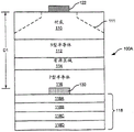
Referring to fig. 5, some embodiments of the present invention provide a light emitting device 100A including a substrate 110 on which an n-type semiconductor layer 112, an active region 114, and a p-type semiconductor layer 116 are formed on the substrate 110. For example, the semiconductor substrate 110 may include a conductive silicon carbide substrate, and the n-type semiconductor layer 112, the active region 114, and the p-type semiconductor layer 116 may include a group III nitride based semiconductor layer. Light emitting device 100A also includes a reduced conductivity region 130 in p-type semiconductor layer 116. As shown in fig. 5, the substrate 110 may include shaped sidewalls 111, which shaped sidewalls 111 may increase the light extraction efficiency from the device 100A by changing the angle at which light generated in the active region 114 strikes the sidewalls of the device 100A. In the structure shown in fig. 5, the reduced conductivity region 130 may be located a distance D1 of about 50 to 400 μm from the pad 122. The reduced conductivity region 130 may be formed by using any of the above-described methods including ion implantation into the p-type semiconductor layer 116.
The light emitting device 100A may be adapted for so-called "flip-chip" mounting on an underlying support. In particular, the semiconductor structure may be mounted on a heat sink, pad, or other surface with the p-type semiconductor layer 116 facing down and the substrate 110 facing up. To facilitate bonding of the light emitting device 100A to the support, a p-type contact metal stack 118 is formed on an exposed surface of the type semiconductor layer 116. Suitable metal stacks For flip chip assembly of optoelectronic devices are disclosed, For example, in U.S. patent publication No.2003/0015721 entitled "Light Emitting diode incorporating Modification For sub-mounting And Manufacturing method For. The disclosure of which is hereby incorporated by reference. In particular, the p-type contact metal stack 118 may include a metal ohmic layer 118A, such as platinum, which metal ohmic layer 118A forms an ohmic contact with the p-type semiconductor layer 116. The metal stack 118 may also include a reflective layer 118B, a barrier layer 118C, and/or a bonding layer 118D.
The bonding layer 118D may include gold and/or tin and may be configured to facilitate thermosonic and/or thermocompressive bonding of the device 100A to a heatsink. The reflective layer 118B may comprise a reflective metal such as silver or aluminum and may be arranged to reflect light away from the heat sink and back into the device 100A so that it may be efficiently extracted. The barrier layer 118C may include a metal such as tungsten, titanium nitride, and/or nickel, and the metal may prevent the metal of the bonding layer 118D from contaminating the ohmic metal 118A and/or the reflector 118B. The Barrier layer may be formed as described in U.S. patent publication No.2005/0194603, entitled "light emitting Diodes incorporating Barrier Layers/substrates And Manufacturing methods for," the disclosure of which is incorporated herein by reference. An optional adhesion layer (not shown) may be disposed between the barrier layer 118C and the bonding layer 118D.
When an optoelectronic device such as the device 100A shown in fig. 5 is mounted on an opaque support member with the p-side of the device 100A facing down (i.e., toward the support), current may spread naturally in the device without the need to form a transparent electrode or current spreading layer on the exposed substrate 110, since the conductivity of the substrate 110 may be sufficiently high. Thus, as shown in fig. 5, the device may include a wire bond pad 122 formed on the substrate 110. Ohmic contacts (not shown) may be formed between the wire bond pads 122 and the substrate 110. In some embodiments, ohmic contacts may be formed self-aligned with the pads 122.
The reduced conductivity region 130 may extend into the p-type semiconductor layer 116 from a surface of the p-type semiconductor layer 116 opposite the active region 114. The reduced conductivity region 130 may extend partially and/or completely through the p-type semiconductor layer 116. In some embodiments, including embodiments having a substrate 110, the reduced conductivity region 130 may extend completely through the active region 114 to/into the n-type semiconductor layer 112. The reduced conductivity region 130 may be formed using techniques such as those described with reference to fig. 1-4. The reduced conductivity region 130 may be formed, for example, by implanting ions through a mask into the p-type semiconductor layer 116 as described above with reference to fig. 2A.
As further illustrated in fig. 5, the reduced conductivity region 130 is generally aligned with the pad 122. The presence of reduced conductivity region 130 may reduce the number of photons generated in device 100A directly beneath wire bond pad 122 because, for example, p-type semiconductor layer 116 may be relatively thin compared to substrate 110, and because current may not readily spread in p-type semiconductor layer 116. Accordingly, the reduced conductivity region 130 may have approximately the same shape as the wire bond pad 122. Additionally, reduced conductivity region 130 may have an area that is approximately the same as, slightly smaller than, or slightly larger than the area of wire bond pad 122. In some embodiments, the reduced conductivity region may have a diameter that is about 6-30 μm larger than the diameter of the wire bond pad 122. Specifically, the pad 122 may have a diameter of about 100-. In embodiments that include a substrate (i.e., where substrate 110 has not been removed), it is desirable to provide reduced conductivity region 130 having an area that is larger than the area of pad 122. For example, if the wire bond pad 122 has a circular shape, the reduced conductivity region 130 may also have a circular shape having an area that is smaller than, about equal to, or slightly larger than the diameter of the wire bond pad 122.
Further embodiments of the present invention are shown in fig. 6A and 6B, which show a light emitting device 100B comprising a p-type semiconductor layer 116, an active region 114 and an n-type semiconductor layer 112. A p-contact metal stack 118 is formed on a surface of the p-type semiconductor layer 116, and a wire pad 122 is formed on a surface of the n-type semiconductor layer 112 opposite the p-type semiconductor layer 116. Specifically, the light emitting device 100B shown in fig. 6A and 6B may not include a substrate.
As further shown in fig. 6A, reduced conductivity region 130 is disposed in p-type semiconductor layer 116 generally in alignment with wire bond pad 122. The reduced conductivity region 130 may extend into the p-type semiconductor layer 116 from a surface of the p-type semiconductor layer 116 opposite the active region 114. The reduced conductivity region 130 may extend partially and/or completely through the p-type semiconductor layer 116. The reduced conductivity region 130 may have an area equal to, greater than, or less than the area of the wire bond pad 122. Reduced conductivity region 130 may be located within device 100B a distance D2 from wire bond pad 122. In some embodiments, the distance D2 may be from 0.3 to 10 μm. In particular, the distance D2 may be about 2 to 3 μm.
Fig. 11A to 11C are schematic plan views of a light emitting device 100B including a wire pad 122 and an aligned reduced conductivity region 130. As shown, reduced conductivity region 130 may have a peripheral shape similar to that of wire bond pad 122, which in the embodiment shown in fig. 11A-11C is generally circular. The wire bond pads 122 and reduced conductivity areas 130 can have other peripheral shapes such as rectangular, star-shaped, cross-shaped, or other shapes or combinations thereof.
As shown in fig. 11A, in some embodiments, reduced conductivity region 130 may have an area slightly larger than the area of wire pad 122, while in other embodiments reduced conductivity region 130 may have an area slightly smaller (fig. 11B) or approximately equal (fig. 11C) than the area of wire pad 122.
Referring to fig. 6B, the reduced conductivity region 130 may extend completely through the p-type semiconductor layer 116 and into the active region 114. In some embodiments, including embodiments without a substrate, the reduced conductivity region 130 may extend completely through the active region 114 into/into the n-type semiconductor layer 112.
In fig. 7A, a further embodiment of the present invention is shown, showing a light emitting device 100C comprising a p-type semiconductor layer 116, an active region 114 and an n-type semiconductor layer 112. The wire bonding pad 122 is formed on the surface of the n-type semiconductor layer 112. A patterned ohmic contact 118 is formed on a surface of the p-type semiconductor layer 116 opposite the n-type semiconductor layer 112. Light emitting device 100C also includes a non-ohmic contact on p-type semiconductor layer 116 opposite wire bond pad 122. In some embodiments, for example, the non-ohmic contact 140 may comprise a rectifying schottky contact. Forming rectifying schottky contacts on nitride-based semiconductor materials is well known to those skilled in the art. In other embodiments, the non-ohmic contact 140 may comprise a non-conductive material, such as silicon dioxide.
The non-ohmic contacts 140 may have approximately the same shape as the wire bond pads 122. Contacts 140 may have an area that is slightly smaller, approximately equal, or slightly larger than the area of wire bond pads 122. Accordingly, when a voltage is applied across the terminals of the device 100C, current may not flow from the non-ohmic contact 140 to the p-type semiconductor layer 116, and the number of photons generated in the active region 114 under the wire bond pad 122 may be reduced.
Referring to fig. 7B, in some embodiments, metal stack 118 may be formed on the surface of p-type semiconductor layer 116 in regions other than reduced conductivity region 150 opposite wire bond pad 122. That is, since the metal stack 118 is not formed in the region 150, the current flowing through the region 150 may be reduced and the number of photons generated in the active layer 114 under the wire bond pad 122 may be reduced when the device is activated.
A further embodiment of the invention is shown in figure 8. In the embodiment of fig. 8, device 100E includes a p-type semiconductor layer 116, an active region 114, and an n-type semiconductor layer 112. A p-type contact 118 is formed on a surface of the p-type semiconductor layer 116 opposite the n-type semiconductor layer 112. A wire pad 122 is formed on a surface of the n-type semiconductor layer 112 opposite to the p-type semiconductor layer 116. An ohmic contact 154 is formed on the same surface of the n-type semiconductor layer 112 as the wire pad 122, and the ohmic contact 154 is electrically connected to the wire pad 122. The ohmic contact may include a transparent material, such as ITO, that forms an ohmic contact with the n-type semiconductor layer 112.
A reduced conductivity region 152 is formed in the n-type semiconductor layer 112 below the wire bond pad 122. The reduced conductivity region 152 may extend from a surface of the n-type semiconductor layer 112 at least partially into the n-type semiconductor layer 112. In some embodiments, the reduced conductivity region 152 may extend completely through the n-type semiconductor layer 112 and into/into the active region 114.
Fig. 9A shows a device 100F according to a further embodiment of the invention. The device 100F also includes a p-type semiconductor layer 116, an active region 114, and an n-type semiconductor layer 112. A p-type contact 118 is formed on a surface of the p-type semiconductor layer 116 opposite the n-type semiconductor layer 112. A wire pad 122 is formed on a surface of the n-type semiconductor layer 112 opposite to the p-type semiconductor layer 116. An ohmic contact 154 is formed on the same surface of the n-type semiconductor layer 112 as the wire pad 122.
A first reduced conductivity region 152 is formed in the n-type semiconductor layer 112 under the wire bond pad 122. The first reduced conductivity region 152 may be aligned with the wire pad 122 and may extend from a surface of the n-type semiconductor layer 112 at least partially into the n-type semiconductor layer 112. In some embodiments, the first reduced conductivity region 152 may extend completely through the n-type semiconductor layer 112 and to/into/through the active region 114.
A second reduced conductivity region 150 is formed in the p-type semiconductor layer 116. The second reduced conductivity region 150 may be aligned with the first reduced conductivity region 152 and/or the wire bond pad 122. The second reduced conductivity region 150 may extend from the surface of the p-type semiconductor layer 116 at least partially into the p-type semiconductor layer 116, and in some cases may extend to/into/through the active region 114.
In embodiments including reduced conductivity regions 150, 152 on both sides of the device, such as the first reduced conductivity region 152 and the second reduced conductivity region 150 of device 100F, the reduced conductivity regions 150, 152 need not be formed using the same technique, but may instead be formed using different techniques, for example. For example, the first reduced conductivity region 152 may be formed via ion implantation, while the second reduced conductivity region 150 may be formed using plasma treatment and or exposure to hydrogen gas, or vice versa. In addition, one or both of the reduced conductivity regions 150, 152 may be formed by forming a non-ohmic material on the surface of the respective semiconductor layer 116, 112 prior to forming electrical contacts thereon, or by not forming an ohmic contact on the surface area of the semiconductor layer corresponding to the pad 122.
Fig. 9B shows a device 100G according to a further embodiment of the invention. The device 100G also includes a p-type semiconductor layer 116, an active region 114, and an n-type semiconductor layer 112. A p-type contact 118 is formed on a surface of the p-type semiconductor layer 116 opposite the n-type semiconductor layer 112. A wire pad 122 is formed on a surface of the n-type semiconductor layer 112 opposite to the p-type semiconductor layer 116. An ohmic contact 154 is formed on the same surface of the n-type semiconductor layer 112 as the wire pad 122.
A reduced conductivity region 152 is formed in the n-type semiconductor layer 112 below the wire bond pad 122. The reduced conductivity region 152 may be aligned with the wire bond pad 122 and may extend from a surface of the n-type semiconductor layer 112 at least partially into the n-type semiconductor layer 112. In some embodiments, the reduced conductivity region 152 may extend completely through the n-type semiconductor layer 112 and to/into/through the active region 114.
A metal contact 118 is formed on a surface of the p-type semiconductor layer 116 opposite the n-type semiconductor layer 112. The metal contact 118 forms an ohmic contact with the p-type semiconductor layer 116 in a region other than the conductivity-reduced region of the surface of the p-type semiconductor layer 116 aligned with the wire pad 122.
Light emitting device 100G also includes a non-ohmic contact 140 on p-type semiconductor layer 116 opposite wire bond pad 122. In some embodiments, for example, the non-ohmic contact 140 may comprise a rectifying schottky contact. In other embodiments, the non-ohmic contact 140 may comprise a non-conductive material such as silicon dioxide.
The non-ohmic contact 140 may have approximately the same shape as the shape of the wire pad 122. Contacts 140 may have an area that is slightly smaller, approximately equal, or slightly larger than the area of wire bond pads 122. In other embodiments, the non-ohmic contacts 140 may include gaps on which no contact is formed.
A further embodiment of the invention is shown in fig. 10, which shows a semiconductor light emitting device 100H including a reduced conductivity region 160, the reduced conductivity region 160 extending from a surface of the n-type semiconductor layer 112 beneath the wire bond pad 122, through the device 100G, and onto an opposite surface of the p-type semiconductor layer 116.
Some of the chip structures in which embodiments of the present invention may be employed are shown equidistantly in fig. 12 and 13. For example, fig. 12 shows a chip structure 100J comprising a carrier substrate 210, such as a silicon substrate, on which the LED structure has been bonded via a metallic bonding layer 220. Between the bonding layer 220 and the LED structure, which includes the p-type semiconductor layer 116, the active layer 114, and the n-type semiconductor layer 112, is the reflective layer 230.
A pair of pads 122 is formed on the surface of the n-type semiconductor layer 112 opposite the substrate 210. The pad 122 is electrically connected to a current spreading structure comprising a plurality of current spreading fingers 154 on the n-type semiconductor layer 112.
An exemplary horizontal chip structure 100K is shown in fig. 13. The chip structure 100K includes a transparent substrate 110 on which an n-type semiconductor layer 112 is formed. A mesa structure including an active region 114 and a p-type semiconductor layer 116 is on the n-type semiconductor layer. A transparent ohmic contact 118, which may comprise ITO, is on the p-type semiconductor layer 116. A pad 122A is on the transparent ohmic contact layer 118 and a current spreading finger 154A extends from the pad 122A. A pad 122B is on the n-type semiconductor layer 112, and a current spreading finger 154B extends from the pad 122B. A reflective layer 23 (fig. 1) may be disposed under the pad 122A and/or the current spreading finger 154A.
Although embodiments of the present invention have been illustrated in fig. 1-13 with reference to specific light emitting device structures, other structures may be provided according to some embodiments of the present invention. Thus, embodiments of the present invention may be provided by any light emitting device comprising one or more current blocking mechanisms as described above. For example, current blocking mechanisms according to some embodiments of the present invention may be provided with reference to exemplary light emitting device structures discussed in the U.S. patents and/or applications incorporated by reference above
Embodiments of the present invention have been described with reference to wire bond pads 22 and 122. As used herein, the term pad includes a light absorbing contact structure. The pads may be single or multi-layered, may be metal and/or metal alloy, and/or may be of uniform or non-uniform composition.
In addition, although embodiments of the present invention have been described with reference to a particular sequence of operations, variations of the above-described sequence may be provided while still benefiting from the teachings of the present invention. Two or more steps may thus be combined into a single step or multiple steps performed in the sequence described herein. For example, the reduced conductivity region may be formed in the semiconductor layer before or after forming the metal layer on the semiconductor layer. Accordingly, embodiments of the invention should not be limited to the specific order of operations described herein unless otherwise specified.
It should be understood by those skilled in the art that various embodiments of the present invention have been described separately in connection with fig. 1-13. However, combinations and subcombinations of the embodiments of fig. 1-13 may be provided according to various embodiments of the invention. As described above, the reduced conductivity region 30 may be used to reduce/prevent carrier recombination in regions of the device where the generated light may be absorbed by some device components, such as pads, current spreading fingers, passivation regions, and the like. Thus, in some embodiments, the reduced conductivity region 30 may be aligned with a light absorbing component and/or region of the device. However, in some cases, it may be desirable to form the reduced conductivity region 30 in other regions that are not aligned with the light absorbing regions or features of the device. For example, it may be desirable to provide reduced conductivity region 30 in a device that causes the device to produce light having a desired far-field emission pattern. Thus, in some embodiments, the reduced conductivity region 30 may be used to shape the light emission pattern of the light emitting device.
In the drawings and specification, there have been disclosed embodiments of the invention and, although specific terms are employed, they are used in a generic and descriptive sense only and not for purposes of limitation, the scope of the invention being set forth in the following claims.
Claims (13)
1. A light emitting device comprising:
a p-type semiconductor layer, an n-type semiconductor layer, and an active region between the n-type semiconductor layer and the p-type semiconductor layer;
an opaque feature on the n-type semiconductor layer opposite the active region; and
a patterned ohmic contact on the p-type semiconductor layer opposite the active region, wherein the patterned ohmic contact is in a region other than a reduced conductivity region of a surface of the p-type semiconductor layer aligned with the opaque member, wherein the light emitting device further comprises a patterned non-ohmic contact on the p-type semiconductor layer, wherein the patterned non-ohmic contact is also aligned with the opaque member.
2. The light emitting device of claim 1, wherein the opaque features comprise pads and/or passivation regions.
3. The light emitting device of claim 1, wherein the opaque members comprise conductive fingers.
4. The light emitting device of claim 1, wherein the patterned non-ohmic contact comprises a metal that does not form an ohmic contact with the p-type semiconductor layer or the patterned non-ohmic contact comprises an insulator.
5. The light emitting device of claim 1, wherein the light emitting device is a vertical light emitting diode.
6. A light emitting device comprising:
a semiconductor diode having a first semiconductor surface and a second semiconductor surface of opposite conductivity types, the first semiconductor surface being opposite the second semiconductor surface;
an opaque member on the first semiconductor surface; and
a patterned ohmic contact on the second semiconductor surface, wherein the patterned ohmic contact is in a region other than a reduced conductivity region of a surface of the p-type semiconductor layer aligned with the opaque feature, wherein the light emitting device further comprises a patterned non-ohmic metal contact on the second semiconductor surface, wherein the patterned non-ohmic metal contact is also aligned with the opaque feature.
7. The light emitting device of claim 6, wherein the opaque features comprise a passivation region.
8. The light emitting device of claim 6, wherein the opaque features comprise conductive fingers.
9. The light emitting device of claim 6, wherein the patterned non-ohmic contact comprises a metal that does not form an ohmic contact with the second semiconductor surface.
10. The light emitting device of claim 6, wherein the light emitting device is a vertical light emitting diode.
11. A light emitting device comprising:
a p-type semiconductor layer, an n-type semiconductor layer, and an active region between the n-type semiconductor layer and the p-type semiconductor layer;
a conductive finger on the n-type semiconductor layer opposite the active region;
a patterned ohmic contact on the p-type semiconductor layer opposite the active region, wherein the patterned ohmic contact is in a region other than a reduced conductivity region of a surface of the p-type semiconductor layer aligned with the conductive finger; and
a patterned non-ohmic contact on the p-type semiconductor layer, wherein the patterned non-ohmic contact is also aligned with the conductive finger.
12. The light emitting device of claim 11, wherein the patterned non-ohmic contact comprises a metal that does not form an ohmic contact with the p-type semiconductor layer or the patterned non-ohmic contact comprises an insulator.
13. The light emitting device of claim 11, wherein the light emitting device is a vertical light emitting diode.
Applications Claiming Priority (3)
| Application Number | Priority Date | Filing Date | Title |
|---|---|---|---|
| US11/715,687 US7795623B2 (en) | 2004-06-30 | 2007-03-08 | Light emitting devices having current reducing structures and methods of forming light emitting devices having current reducing structures |
| US11/715,687 | 2007-03-08 | ||
| CN200880015255A CN101681961A (en) | 2007-03-08 | 2008-02-19 | Light emitting devices having current reducing structures and methods of forming light emitting devices having current reducing structures |
Related Parent Applications (1)
| Application Number | Title | Priority Date | Filing Date |
|---|---|---|---|
| CN200880015255A Division CN101681961A (en) | 2007-03-08 | 2008-02-19 | Light emitting devices having current reducing structures and methods of forming light emitting devices having current reducing structures |
Publications (2)
| Publication Number | Publication Date |
|---|---|
| CN105098012A CN105098012A (en) | 2015-11-25 |
| CN105098012B true CN105098012B (en) | 2020-05-15 |
Family
ID=39428041
Family Applications (2)
| Application Number | Title | Priority Date | Filing Date |
|---|---|---|---|
| CN201510512428.9A Active CN105098012B (en) | 2007-03-08 | 2008-02-19 | Light emitting device and method of manufacturing the same |
| CN200880015255A Pending CN101681961A (en) | 2007-03-08 | 2008-02-19 | Light emitting devices having current reducing structures and methods of forming light emitting devices having current reducing structures |
Family Applications After (1)
| Application Number | Title | Priority Date | Filing Date |
|---|---|---|---|
| CN200880015255A Pending CN101681961A (en) | 2007-03-08 | 2008-02-19 | Light emitting devices having current reducing structures and methods of forming light emitting devices having current reducing structures |
Country Status (6)
| Country | Link |
|---|---|
| US (4) | US7795623B2 (en) |
| EP (2) | EP3264475B1 (en) |
| JP (1) | JP5693852B2 (en) |
| KR (3) | KR20140103337A (en) |
| CN (2) | CN105098012B (en) |
| WO (1) | WO2008112064A2 (en) |
Families Citing this family (113)
| Publication number | Priority date | Publication date | Assignee | Title |
|---|---|---|---|---|
| TWI294699B (en) * | 2006-01-27 | 2008-03-11 | Epistar Corp | Light emitting device and method of forming the same |
| CN101556985B (en) | 2003-04-30 | 2017-06-09 | 克利公司 | High powered light emitter encapsulation with compact optical element |
| US7534633B2 (en) * | 2004-07-02 | 2009-05-19 | Cree, Inc. | LED with substrate modifications for enhanced light extraction and method of making same |
| US8698184B2 (en) | 2011-01-21 | 2014-04-15 | Cree, Inc. | Light emitting diodes with low junction temperature and solid state backlight components including light emitting diodes with low junction temperature |
| KR100867529B1 (en) * | 2006-11-14 | 2008-11-10 | 삼성전기주식회사 | Vertical light emitting device |
| US8878245B2 (en) * | 2006-11-30 | 2014-11-04 | Cree, Inc. | Transistors and method for making ohmic contact to transistors |
| US8021904B2 (en) * | 2007-02-01 | 2011-09-20 | Cree, Inc. | Ohmic contacts to nitrogen polarity GaN |
| US9484499B2 (en) * | 2007-04-20 | 2016-11-01 | Cree, Inc. | Transparent ohmic contacts on light emitting diodes with carrier substrates |
| US11114594B2 (en) | 2007-08-24 | 2021-09-07 | Creeled, Inc. | Light emitting device packages using light scattering particles of different size |
| US9461201B2 (en) | 2007-11-14 | 2016-10-04 | Cree, Inc. | Light emitting diode dielectric mirror |
| US8536584B2 (en) * | 2007-11-14 | 2013-09-17 | Cree, Inc. | High voltage wire bond free LEDS |
| US9754926B2 (en) | 2011-01-31 | 2017-09-05 | Cree, Inc. | Light emitting diode (LED) arrays including direct die attach and related assemblies |
| US8368100B2 (en) | 2007-11-14 | 2013-02-05 | Cree, Inc. | Semiconductor light emitting diodes having reflective structures and methods of fabricating same |
| US9634191B2 (en) * | 2007-11-14 | 2017-04-25 | Cree, Inc. | Wire bond free wafer level LED |
| US8575633B2 (en) | 2008-12-08 | 2013-11-05 | Cree, Inc. | Light emitting diode with improved light extraction |
| US9660153B2 (en) | 2007-11-14 | 2017-05-23 | Cree, Inc. | Gap engineering for flip-chip mounted horizontal LEDs |
| US7915629B2 (en) | 2008-12-08 | 2011-03-29 | Cree, Inc. | Composite high reflectivity layer |
| US9431589B2 (en) * | 2007-12-14 | 2016-08-30 | Cree, Inc. | Textured encapsulant surface in LED packages |
| US8058088B2 (en) | 2008-01-15 | 2011-11-15 | Cree, Inc. | Phosphor coating systems and methods for light emitting structures and packaged light emitting diodes including phosphor coating |
| US8940561B2 (en) * | 2008-01-15 | 2015-01-27 | Cree, Inc. | Systems and methods for application of optical materials to optical elements |
| JP5126884B2 (en) * | 2008-01-16 | 2013-01-23 | シャープ株式会社 | Nitride semiconductor light emitting device and method for manufacturing nitride semiconductor light emitting device |
| CN102037575B (en) * | 2008-03-27 | 2013-04-10 | 宋俊午 | Light-emitting element and a production method therefor |
| US20090242929A1 (en) * | 2008-03-31 | 2009-10-01 | Chao-Kun Lin | Light emitting diodes with patterned current blocking metal contact |
| EP2280426B1 (en) * | 2008-04-16 | 2017-07-05 | LG Innotek Co., Ltd. | Light-emitting device |
| CN102017200B (en) * | 2008-04-25 | 2013-07-10 | Lg伊诺特有限公司 | Light-emitting element and a production method therefor |
| US8664747B2 (en) * | 2008-04-28 | 2014-03-04 | Toshiba Techno Center Inc. | Trenched substrate for crystal growth and wafer bonding |
| US8154038B2 (en) * | 2008-07-01 | 2012-04-10 | Taiwan Semiconductor Manufacturing Co., Ltd | Group-III nitride for reducing stress caused by metal nitride reflector |
| US8384115B2 (en) * | 2008-08-01 | 2013-02-26 | Cree, Inc. | Bond pad design for enhancing light extraction from LED chips |
| KR101047634B1 (en) | 2008-11-24 | 2011-07-07 | 엘지이노텍 주식회사 | Light emitting device and manufacturing method |
| US8017963B2 (en) * | 2008-12-08 | 2011-09-13 | Cree, Inc. | Light emitting diode with a dielectric mirror having a lateral configuration |
| KR101134720B1 (en) * | 2009-02-16 | 2012-04-13 | 엘지이노텍 주식회사 | Semiconductor light emitting device and fabrication method thereof |
| US8476668B2 (en) * | 2009-04-06 | 2013-07-02 | Cree, Inc. | High voltage low current surface emitting LED |
| US8529102B2 (en) | 2009-04-06 | 2013-09-10 | Cree, Inc. | Reflector system for lighting device |
| US9093293B2 (en) | 2009-04-06 | 2015-07-28 | Cree, Inc. | High voltage low current surface emitting light emitting diode |
| US8741715B2 (en) * | 2009-04-29 | 2014-06-03 | Cree, Inc. | Gate electrodes for millimeter-wave operation and methods of fabrication |
| KR100999726B1 (en) * | 2009-05-04 | 2010-12-08 | 엘지이노텍 주식회사 | Light emitting device and method for fabricating the same |
| KR20100122998A (en) * | 2009-05-14 | 2010-11-24 | 엘지이노텍 주식회사 | Light emitting device and method for fabricating the same |
| US8207547B2 (en) * | 2009-06-10 | 2012-06-26 | Brudgelux, Inc. | Thin-film LED with P and N contacts electrically isolated from the substrate |
| TWI405409B (en) * | 2009-08-27 | 2013-08-11 | Novatek Microelectronics Corp | Low voltage differential signal output stage |
| KR101154750B1 (en) * | 2009-09-10 | 2012-06-08 | 엘지이노텍 주식회사 | Light emitting device and method for fabricating the same |
| TWI398965B (en) * | 2009-11-25 | 2013-06-11 | Formosa Epitaxy Inc | Light emitting diode chip and package structure thereof |
| US8525221B2 (en) | 2009-11-25 | 2013-09-03 | Toshiba Techno Center, Inc. | LED with improved injection efficiency |
| KR101091304B1 (en) * | 2010-01-20 | 2011-12-07 | 엘지이노텍 주식회사 | Light emitting device package and fabricating method thereof |
| KR101014155B1 (en) | 2010-03-10 | 2011-02-10 | 엘지이노텍 주식회사 | Light emitting device, method for fabricating the light emitting device and light emitting device package |
| KR101054984B1 (en) * | 2010-03-26 | 2011-08-05 | 엘지이노텍 주식회사 | Light emitting device, method for fabricating the light emitting device and light emitting device package |
| US9105824B2 (en) | 2010-04-09 | 2015-08-11 | Cree, Inc. | High reflective board or substrate for LEDs |
| US8263422B2 (en) * | 2010-04-26 | 2012-09-11 | Varian Semiconductor Equipment Associates, Inc. | Bond pad isolation and current confinement in an LED using ion implantation |
| US8154042B2 (en) | 2010-04-29 | 2012-04-10 | Koninklijke Philips Electronics N V | Light emitting device with trenches and a top contact |
| US8329482B2 (en) | 2010-04-30 | 2012-12-11 | Cree, Inc. | White-emitting LED chips and method for making same |
| KR101525913B1 (en) * | 2010-06-22 | 2015-06-10 | 순천대학교 산학협력단 | Verticle light emitting diodes and its fabricating method |
| US8764224B2 (en) | 2010-08-12 | 2014-07-01 | Cree, Inc. | Luminaire with distributed LED sources |
| US8502244B2 (en) | 2010-08-31 | 2013-08-06 | Micron Technology, Inc. | Solid state lighting devices with current routing and associated methods of manufacturing |
| US9070851B2 (en) | 2010-09-24 | 2015-06-30 | Seoul Semiconductor Co., Ltd. | Wafer-level light emitting diode package and method of fabricating the same |
| US8455882B2 (en) | 2010-10-15 | 2013-06-04 | Cree, Inc. | High efficiency LEDs |
| US8556469B2 (en) | 2010-12-06 | 2013-10-15 | Cree, Inc. | High efficiency total internal reflection optic for solid state lighting luminaires |
| US9673363B2 (en) | 2011-01-31 | 2017-06-06 | Cree, Inc. | Reflective mounting substrates for flip-chip mounted horizontal LEDs |
| US9831220B2 (en) | 2011-01-31 | 2017-11-28 | Cree, Inc. | Light emitting diode (LED) arrays including direct die attach and related assemblies |
| US9508904B2 (en) | 2011-01-31 | 2016-11-29 | Cree, Inc. | Structures and substrates for mounting optical elements and methods and devices for providing the same background |
| US9053958B2 (en) | 2011-01-31 | 2015-06-09 | Cree, Inc. | Light emitting diode (LED) arrays including direct die attach and related assemblies |
| US9166126B2 (en) | 2011-01-31 | 2015-10-20 | Cree, Inc. | Conformally coated light emitting devices and methods for providing the same |
| US9401103B2 (en) | 2011-02-04 | 2016-07-26 | Cree, Inc. | LED-array light source with aspect ratio greater than 1 |
| US9362455B2 (en) * | 2011-02-24 | 2016-06-07 | Cree, Inc. | Semiconductor light emitting diodes having multiple bond pads and current spreading structures |
| JP5433609B2 (en) | 2011-03-03 | 2014-03-05 | 株式会社東芝 | Semiconductor light emitting device and manufacturing method thereof |
| JP2012186195A (en) | 2011-03-03 | 2012-09-27 | Toshiba Corp | Semiconductor light-emitting element and method of manufacturing the same |
| US8680556B2 (en) | 2011-03-24 | 2014-03-25 | Cree, Inc. | Composite high reflectivity layer |
| JP4989773B1 (en) * | 2011-05-16 | 2012-08-01 | 株式会社東芝 | Semiconductor light emitting device |
| US8686429B2 (en) | 2011-06-24 | 2014-04-01 | Cree, Inc. | LED structure with enhanced mirror reflectivity |
| US9728676B2 (en) | 2011-06-24 | 2017-08-08 | Cree, Inc. | High voltage monolithic LED chip |
| US10243121B2 (en) | 2011-06-24 | 2019-03-26 | Cree, Inc. | High voltage monolithic LED chip with improved reliability |
| US8395165B2 (en) | 2011-07-08 | 2013-03-12 | Bridelux, Inc. | Laterally contacted blue LED with superlattice current spreading layer |
| US20130026480A1 (en) | 2011-07-25 | 2013-01-31 | Bridgelux, Inc. | Nucleation of Aluminum Nitride on a Silicon Substrate Using an Ammonia Preflow |
| US8916906B2 (en) | 2011-07-29 | 2014-12-23 | Kabushiki Kaisha Toshiba | Boron-containing buffer layer for growing gallium nitride on silicon |
| US8865565B2 (en) | 2011-08-02 | 2014-10-21 | Kabushiki Kaisha Toshiba | LED having a low defect N-type layer that has grown on a silicon substrate |
| US9343641B2 (en) | 2011-08-02 | 2016-05-17 | Manutius Ip, Inc. | Non-reactive barrier metal for eutectic bonding process |
| US9012939B2 (en) | 2011-08-02 | 2015-04-21 | Kabushiki Kaisha Toshiba | N-type gallium-nitride layer having multiple conductive intervening layers |
| US9142743B2 (en) | 2011-08-02 | 2015-09-22 | Kabushiki Kaisha Toshiba | High temperature gold-free wafer bonding for light emitting diodes |
| US20130032810A1 (en) | 2011-08-03 | 2013-02-07 | Bridgelux, Inc. | Led on silicon substrate using zinc-sulfide as buffer layer |
| US8564010B2 (en) | 2011-08-04 | 2013-10-22 | Toshiba Techno Center Inc. | Distributed current blocking structures for light emitting diodes |
| US8624482B2 (en) | 2011-09-01 | 2014-01-07 | Toshiba Techno Center Inc. | Distributed bragg reflector for reflecting light of multiple wavelengths from an LED |
| US8669585B1 (en) | 2011-09-03 | 2014-03-11 | Toshiba Techno Center Inc. | LED that has bounding silicon-doped regions on either side of a strain release layer |
| US8558247B2 (en) | 2011-09-06 | 2013-10-15 | Toshiba Techno Center Inc. | GaN LEDs with improved area and method for making the same |
| US8686430B2 (en) | 2011-09-07 | 2014-04-01 | Toshiba Techno Center Inc. | Buffer layer for GaN-on-Si LED |
| US20130082274A1 (en) | 2011-09-29 | 2013-04-04 | Bridgelux, Inc. | Light emitting devices having dislocation density maintaining buffer layers |
| US8853668B2 (en) | 2011-09-29 | 2014-10-07 | Kabushiki Kaisha Toshiba | Light emitting regions for use with light emitting devices |
| US9178114B2 (en) | 2011-09-29 | 2015-11-03 | Manutius Ip, Inc. | P-type doping layers for use with light emitting devices |
| US8698163B2 (en) | 2011-09-29 | 2014-04-15 | Toshiba Techno Center Inc. | P-type doping layers for use with light emitting devices |
| US9012921B2 (en) | 2011-09-29 | 2015-04-21 | Kabushiki Kaisha Toshiba | Light emitting devices having light coupling layers |
| US8664679B2 (en) | 2011-09-29 | 2014-03-04 | Toshiba Techno Center Inc. | Light emitting devices having light coupling layers with recessed electrodes |
| JP2013093412A (en) * | 2011-10-25 | 2013-05-16 | Showa Denko Kk | Light emitting diode, manufacturing method of light emitting diode, light emitting diode lamp, and lighting device |
| US9312437B2 (en) * | 2011-11-07 | 2016-04-12 | Koninklijke Philips N.V. | P-contact with more uniform injection and lower optical loss |
| KR101219290B1 (en) * | 2011-11-08 | 2013-01-21 | 순천대학교 산학협력단 | Method for fabricating light emitting diodes |
| US8581267B2 (en) | 2011-11-09 | 2013-11-12 | Toshiba Techno Center Inc. | Series connected segmented LED |
| US8552465B2 (en) | 2011-11-09 | 2013-10-08 | Toshiba Techno Center Inc. | Method for reducing stress in epitaxial growth |
| US20130214294A1 (en) | 2012-02-17 | 2013-08-22 | Epistar Corporation | Light emitting device with planar current block structure |
| US20130221320A1 (en) * | 2012-02-27 | 2013-08-29 | Tsmc Solid State Lighting Ltd. | Led with embedded doped current blocking layer |
| JP5694215B2 (en) * | 2012-03-07 | 2015-04-01 | 株式会社東芝 | Semiconductor light emitting device |
| US9450152B2 (en) * | 2012-05-29 | 2016-09-20 | Micron Technology, Inc. | Solid state transducer dies having reflective features over contacts and associated systems and methods |
| KR101929891B1 (en) * | 2012-06-08 | 2018-12-17 | 엘지이노텍 주식회사 | Light emitting device, light emitting device package, and light unit |
| CN102779914A (en) * | 2012-08-01 | 2012-11-14 | 厦门市三安光电科技有限公司 | Vertical light-emitting diode with current blocking effect and manufacturing method thereof |
| TWI533472B (en) | 2012-09-12 | 2016-05-11 | 聯勝光電股份有限公司 | Semiconductor light emitting device and fabricating method thereof |
| US9196798B2 (en) | 2012-09-12 | 2015-11-24 | High Power Opto. Inc. | Semiconductor light-emitting device and fabricating method thereof |
| KR101482526B1 (en) * | 2012-12-28 | 2015-01-16 | 일진엘이디(주) | Method of manufacturing nitride semiconductor light emitting device |
| TWI478387B (en) * | 2013-10-23 | 2015-03-21 | Lextar Electronics Corp | Light emitting diode structure |
| KR102153123B1 (en) * | 2014-06-10 | 2020-10-26 | 엘지이노텍 주식회사 | Light emitting deviceand light emitting device package thereof |
| CN107210337B (en) | 2014-11-06 | 2021-06-29 | 亮锐控股有限公司 | Light emitting device with trench under top contact |
| CN104409595B (en) * | 2014-12-03 | 2017-05-03 | 佛山市国星半导体技术有限公司 | Vertical light emitting diode (LED) with current blocking structures and manufacturing method thereof |
| USD826871S1 (en) | 2014-12-11 | 2018-08-28 | Cree, Inc. | Light emitting diode device |
| US10658546B2 (en) | 2015-01-21 | 2020-05-19 | Cree, Inc. | High efficiency LEDs and methods of manufacturing |
| CN205944139U (en) | 2016-03-30 | 2017-02-08 | 首尔伟傲世有限公司 | Ultraviolet ray light -emitting diode spare and contain this emitting diode module |
| KR102386513B1 (en) * | 2016-08-05 | 2022-04-22 | 서울바이오시스 주식회사 | Light emitting device |
| US10763389B1 (en) * | 2019-06-11 | 2020-09-01 | Facebook Technologies, Llc | LED structure with minimized light emission area |
| US11101418B1 (en) | 2019-09-10 | 2021-08-24 | Facebook Technologies, Llc | Spacer for self-aligned mesa |
| US11164995B2 (en) | 2020-02-20 | 2021-11-02 | Facebook Technologies, Llc | 3-D structure for increasing contact surface area for LEDs |
Family Cites Families (125)
| Publication number | Priority date | Publication date | Assignee | Title |
|---|---|---|---|---|
| US4866005A (en) | 1987-10-26 | 1989-09-12 | North Carolina State University | Sublimation of silicon carbide to produce large, device quality single crystals of silicon carbide |
| US4864370A (en) * | 1987-11-16 | 1989-09-05 | Motorola, Inc. | Electrical contact for an LED |
| JPH0682862B2 (en) * | 1988-01-29 | 1994-10-19 | 日立電線株式会社 | Light emitting diode |
| JPH0278280A (en) | 1988-09-14 | 1990-03-19 | Ricoh Co Ltd | Semiconductor light emitting device |
| US5027168A (en) | 1988-12-14 | 1991-06-25 | Cree Research, Inc. | Blue light emitting diode formed in silicon carbide |
| US4918497A (en) | 1988-12-14 | 1990-04-17 | Cree Research, Inc. | Blue light emitting diode formed in silicon carbide |
| JP3117203B2 (en) | 1989-08-31 | 2000-12-11 | 株式会社東芝 | Light emitting diode and method of manufacturing the same |
| US5153889A (en) | 1989-05-31 | 1992-10-06 | Kabushiki Kaisha Toshiba | Semiconductor light emitting device |
| US5048035A (en) | 1989-05-31 | 1991-09-10 | Kabushiki Kaisha Toshiba | Semiconductor light emitting device |
| US4966862A (en) | 1989-08-28 | 1990-10-30 | Cree Research, Inc. | Method of production of light emitting diodes |
| US4946547A (en) | 1989-10-13 | 1990-08-07 | Cree Research, Inc. | Method of preparing silicon carbide surfaces for crystal growth |
| US5210051A (en) | 1990-03-27 | 1993-05-11 | Cree Research, Inc. | High efficiency light emitting diodes from bipolar gallium nitride |
| US5200022A (en) | 1990-10-03 | 1993-04-06 | Cree Research, Inc. | Method of improving mechanically prepared substrate surfaces of alpha silicon carbide for deposition of beta silicon carbide thereon and resulting product |
| JPH04264781A (en) | 1991-02-20 | 1992-09-21 | Eastman Kodak Japan Kk | Light-emitting diode array |
| JP2856374B2 (en) | 1992-02-24 | 1999-02-10 | シャープ株式会社 | Semiconductor light emitting device and method of manufacturing the same |
| JP2798545B2 (en) | 1992-03-03 | 1998-09-17 | シャープ株式会社 | Semiconductor light emitting device and method of manufacturing the same |
| US5245622A (en) | 1992-05-07 | 1993-09-14 | Bandgap Technology Corporation | Vertical-cavity surface-emitting lasers with intra-cavity structures |
| DE4305296C3 (en) | 1993-02-20 | 1999-07-15 | Vishay Semiconductor Gmbh | Method of manufacturing a radiation emitting diode |
| US5416342A (en) | 1993-06-23 | 1995-05-16 | Cree Research, Inc. | Blue light-emitting diode with high external quantum efficiency |
| JPH0722646A (en) | 1993-06-30 | 1995-01-24 | Mitsubishi Chem Corp | Led with current block layer |
| US5338944A (en) | 1993-09-22 | 1994-08-16 | Cree Research, Inc. | Blue light-emitting diode with degenerate junction structure |
| JPH0794778A (en) * | 1993-09-22 | 1995-04-07 | Olympus Optical Co Ltd | Light emitting device |
| DE4338187A1 (en) | 1993-11-09 | 1995-05-11 | Telefunken Microelectron | Light-emitting semiconductor component |
| JP3316062B2 (en) | 1993-12-09 | 2002-08-19 | 株式会社東芝 | Semiconductor light emitting device |
| US5393993A (en) | 1993-12-13 | 1995-02-28 | Cree Research, Inc. | Buffer structure between silicon carbide and gallium nitride and resulting semiconductor devices |
| US5604135A (en) | 1994-08-12 | 1997-02-18 | Cree Research, Inc. | Method of forming green light emitting diode in silicon carbide |
| US5523589A (en) | 1994-09-20 | 1996-06-04 | Cree Research, Inc. | Vertical geometry light emitting diode with group III nitride active layer and extended lifetime |
| US5631190A (en) | 1994-10-07 | 1997-05-20 | Cree Research, Inc. | Method for producing high efficiency light-emitting diodes and resulting diode structures |
| JPH08222797A (en) | 1995-01-17 | 1996-08-30 | Hewlett Packard Co <Hp> | Semiconductor device and manufacture thereof |
| US5814839A (en) | 1995-02-16 | 1998-09-29 | Sharp Kabushiki Kaisha | Semiconductor light-emitting device having a current adjusting layer and a uneven shape light emitting region, and method for producing same |
| JPH08250768A (en) | 1995-03-13 | 1996-09-27 | Toyoda Gosei Co Ltd | Semiconductor optical element |
| US5739554A (en) | 1995-05-08 | 1998-04-14 | Cree Research, Inc. | Double heterojunction light emitting diode with gallium nitride active layer |
| US5565694A (en) | 1995-07-10 | 1996-10-15 | Huang; Kuo-Hsin | Light emitting diode with current blocking layer |
| DE19629920B4 (en) | 1995-08-10 | 2006-02-02 | LumiLeds Lighting, U.S., LLC, San Jose | Light-emitting diode with a non-absorbing distributed Bragg reflector |
| US5719891A (en) | 1995-12-18 | 1998-02-17 | Picolight Incorporated | Conductive element with lateral oxidation barrier |
| US5779924A (en) | 1996-03-22 | 1998-07-14 | Hewlett-Packard Company | Ordered interface texturing for a light emitting device |
| JPH10294531A (en) | 1997-02-21 | 1998-11-04 | Toshiba Corp | Nitride compound semiconductor light emitting element |
| US6057562A (en) | 1997-04-18 | 2000-05-02 | Epistar Corp. | High efficiency light emitting diode with distributed Bragg reflector |
| US6420735B2 (en) | 1997-05-07 | 2002-07-16 | Samsung Electronics Co., Ltd. | Surface-emitting light-emitting diode |
| US5789768A (en) | 1997-06-23 | 1998-08-04 | Epistar Corporation | Light emitting diode having transparent conductive oxide formed on the contact layer |
| US6201262B1 (en) | 1997-10-07 | 2001-03-13 | Cree, Inc. | Group III nitride photonic devices on silicon carbide substrates with conductive buffer interlay structure |
| DE19745723A1 (en) | 1997-10-16 | 1998-12-10 | Telefunken Microelectron | Light emitting semiconductor device especially LED |
| JPH11135834A (en) | 1997-10-27 | 1999-05-21 | Matsushita Electric Ind Co Ltd | Light-emitting diode device and manufacture thereof |
| EP0926744B8 (en) | 1997-12-15 | 2008-05-21 | Philips Lumileds Lighting Company, LLC. | Light emitting device |
| JP3516434B2 (en) | 1997-12-25 | 2004-04-05 | 昭和電工株式会社 | Compound semiconductor light emitting device |
| JPH11204833A (en) | 1998-01-08 | 1999-07-30 | Pioneer Electron Corp | Manufacture of semiconductor light emitting device |
| JP3653384B2 (en) | 1998-02-10 | 2005-05-25 | シャープ株式会社 | Manufacturing method of light emitting diode |
| US6291839B1 (en) | 1998-09-11 | 2001-09-18 | Lulileds Lighting, U.S. Llc | Light emitting device having a finely-patterned reflective contact |
| US6177688B1 (en) | 1998-11-24 | 2001-01-23 | North Carolina State University | Pendeoepitaxial gallium nitride semiconductor layers on silcon carbide substrates |
| US6376269B1 (en) | 1999-02-02 | 2002-04-23 | Agilent Technologies, Inc. | Vertical cavity surface emitting laser (VCSEL) using buried Bragg reflectors and method for producing same |
| JP2000261029A (en) | 1999-03-12 | 2000-09-22 | Oki Electric Ind Co Ltd | Optical semiconductor element |
| JP2000294837A (en) | 1999-04-05 | 2000-10-20 | Stanley Electric Co Ltd | Gallium nitride compound semiconductor light emitting element |
| US6222207B1 (en) | 1999-05-24 | 2001-04-24 | Lumileds Lighting, U.S. Llc | Diffusion barrier for increased mirror reflectivity in reflective solderable contacts on high power LED chip |
| TW437104B (en) | 1999-05-25 | 2001-05-28 | Wang Tien Yang | Semiconductor light-emitting device and method for manufacturing the same |
| US6287947B1 (en) | 1999-06-08 | 2001-09-11 | Lumileds Lighting, U.S. Llc | Method of forming transparent contacts to a p-type GaN layer |
| US6133589A (en) | 1999-06-08 | 2000-10-17 | Lumileds Lighting, U.S., Llc | AlGaInN-based LED having thick epitaxial layer for improved light extraction |
| JP2001077414A (en) | 1999-09-07 | 2001-03-23 | Showa Denko Kk | Group iii nitride semiconductor light-emitting diode |
| US6534798B1 (en) | 1999-09-08 | 2003-03-18 | California Institute Of Technology | Surface plasmon enhanced light emitting diode and method of operation for the same |
| JP2001085742A (en) | 1999-09-17 | 2001-03-30 | Toshiba Corp | Semiconductor light emitting element and its manufacturing method |
| JP2001111103A (en) * | 1999-10-14 | 2001-04-20 | Korai Kagi Kofun Yugenkoshi | Region current density controllable led |
| US6492661B1 (en) | 1999-11-04 | 2002-12-10 | Fen-Ren Chien | Light emitting semiconductor device having reflection layer structure |
| US6812502B1 (en) | 1999-11-04 | 2004-11-02 | Uni Light Technology Incorporation | Flip-chip light-emitting device |
| US6410942B1 (en) | 1999-12-03 | 2002-06-25 | Cree Lighting Company | Enhanced light extraction through the use of micro-LED arrays |
| EP1234344B1 (en) | 1999-12-03 | 2020-12-02 | Cree, Inc. | Enhanced light extraction in leds through the use of internal and external optical elements |
| US6992334B1 (en) | 1999-12-22 | 2006-01-31 | Lumileds Lighting U.S., Llc | Multi-layer highly reflective ohmic contacts for semiconductor devices |
| US6514782B1 (en) | 1999-12-22 | 2003-02-04 | Lumileds Lighting, U.S., Llc | Method of making a III-nitride light-emitting device with increased light generating capability |
| US6486499B1 (en) | 1999-12-22 | 2002-11-26 | Lumileds Lighting U.S., Llc | III-nitride light-emitting device with increased light generating capability |
| JP2001274456A (en) | 2000-01-18 | 2001-10-05 | Sharp Corp | Light emitting diode |
| US6455343B1 (en) * | 2000-03-28 | 2002-09-24 | United Epitaxy Company, Ltd. | Method of manufacturing light emitting diode with current blocking structure |
| JP3975388B2 (en) | 2000-04-07 | 2007-09-12 | サンケン電気株式会社 | Semiconductor light emitting device |
| CN1292494C (en) | 2000-04-26 | 2006-12-27 | 奥斯兰姆奥普托半导体有限责任公司 | Radiation-emitting semiconductor element and method for producing same |
| US6420732B1 (en) * | 2000-06-26 | 2002-07-16 | Luxnet Corporation | Light emitting diode of improved current blocking and light extraction structure |
| JP2002026386A (en) * | 2000-07-10 | 2002-01-25 | Toyoda Gosei Co Ltd | Iii nitride compound semiconductor light emitting element |
| JP2002064221A (en) | 2000-08-18 | 2002-02-28 | Hitachi Cable Ltd | Light-emitting diode |
| TW461124B (en) | 2000-11-14 | 2001-10-21 | Advanced Epitaxy Technology In | Light emitting diode device with high light transmittance |
| US6905900B1 (en) | 2000-11-28 | 2005-06-14 | Finisar Corporation | Versatile method and system for single mode VCSELs |
| US6791119B2 (en) | 2001-02-01 | 2004-09-14 | Cree, Inc. | Light emitting diodes including modifications for light extraction |
| US6468824B2 (en) * | 2001-03-22 | 2002-10-22 | Uni Light Technology Inc. | Method for forming a semiconductor device having a metallic substrate |
| JP2002329885A (en) * | 2001-05-01 | 2002-11-15 | Rohm Co Ltd | Semiconductor light emitting device |
| US6958497B2 (en) | 2001-05-30 | 2005-10-25 | Cree, Inc. | Group III nitride based light emitting diode structures with a quantum well and superlattice, group III nitride based quantum well structures and group III nitride based superlattice structures |
| JP2003017748A (en) | 2001-06-27 | 2003-01-17 | Seiwa Electric Mfg Co Ltd | Gallium nitride-based compound semiconductor light emitting element and manufacturing method therefor |
| JP4058590B2 (en) | 2001-06-29 | 2008-03-12 | サンケン電気株式会社 | Semiconductor light emitting device |
| US7501023B2 (en) | 2001-07-06 | 2009-03-10 | Technologies And Devices, International, Inc. | Method and apparatus for fabricating crack-free Group III nitride semiconductor materials |
| US7211833B2 (en) | 2001-07-23 | 2007-05-01 | Cree, Inc. | Light emitting diodes including barrier layers/sublayers |
| US6740906B2 (en) * | 2001-07-23 | 2004-05-25 | Cree, Inc. | Light emitting diodes including modifications for submount bonding |
| JP4055503B2 (en) | 2001-07-24 | 2008-03-05 | 日亜化学工業株式会社 | Semiconductor light emitting device |
| JP2003037285A (en) | 2001-07-25 | 2003-02-07 | Hitachi Cable Ltd | Light-emitting diode |
| JP2003168823A (en) | 2001-09-18 | 2003-06-13 | Toyoda Gosei Co Ltd | Iii nitride based compound semiconductor light emitting element |
| JP4089194B2 (en) | 2001-09-28 | 2008-05-28 | 日亜化学工業株式会社 | Nitride semiconductor light emitting diode |
| US7148520B2 (en) | 2001-10-26 | 2006-12-12 | Lg Electronics Inc. | Diode having vertical structure and method of manufacturing the same |
| TWI276230B (en) | 2001-12-04 | 2007-03-11 | Epitech Corp Ltd | Structure and manufacturing method of light emitting diode |
| US6784462B2 (en) | 2001-12-13 | 2004-08-31 | Rensselaer Polytechnic Institute | Light-emitting diode with planar omni-directional reflector |
| WO2003061021A2 (en) | 2001-12-21 | 2003-07-24 | Regents Of The University Of California, The Office Of Technology Transfer | Implantation for current confinement in nitride-based vertical optoelectronics |
| TW513820B (en) | 2001-12-26 | 2002-12-11 | United Epitaxy Co Ltd | Light emitting diode and its manufacturing method |
| US6738409B2 (en) | 2001-12-28 | 2004-05-18 | Honeywell International Inc. | Current confinement, capacitance reduction and isolation of VCSELs using deep elemental traps |
| JP4207781B2 (en) | 2002-01-28 | 2009-01-14 | 日亜化学工業株式会社 | Nitride semiconductor device having supporting substrate and method for manufacturing the same |
| JP3975763B2 (en) * | 2002-01-30 | 2007-09-12 | 昭和電工株式会社 | Boron phosphide-based semiconductor light-emitting device, manufacturing method thereof, and light-emitting diode |
| TW513821B (en) | 2002-02-01 | 2002-12-11 | Hsiu-Hen Chang | Electrode structure of LED and manufacturing the same |
| US6919585B2 (en) | 2002-05-17 | 2005-07-19 | Lumei Optoelectronics, Inc. | Light-emitting diode with silicon carbide substrate |
| US6828596B2 (en) | 2002-06-13 | 2004-12-07 | Lumileds Lighting U.S., Llc | Contacting scheme for large and small area semiconductor light emitting flip chip devices |
| JP2004047760A (en) | 2002-07-12 | 2004-02-12 | Hitachi Cable Ltd | Light emitting diode and epitaxial wafer therefor |
| AU2003263779A1 (en) | 2002-07-22 | 2004-02-09 | Cree, Inc. | Light emitting diode including barrier layers and manufacturing methods therefor |
| JP2006500767A (en) | 2002-09-19 | 2006-01-05 | クリー インコーポレイテッド | Light emitting diode and manufacturing method thereof |
| JP2004165436A (en) | 2002-11-13 | 2004-06-10 | Rohm Co Ltd | Method of manufacturing semiconductor light emitting device |
| JP2004172189A (en) | 2002-11-18 | 2004-06-17 | Shiro Sakai | Nitride semiconductor device and its manufacturing method |
| TW200409378A (en) | 2002-11-25 | 2004-06-01 | Super Nova Optoelectronics Corp | GaN-based light-emitting diode and the manufacturing method thereof |
| JP4159865B2 (en) | 2002-12-11 | 2008-10-01 | シャープ株式会社 | Nitride compound semiconductor light emitting device manufacturing method |
| JP3720341B2 (en) | 2003-02-12 | 2005-11-24 | ローム株式会社 | Semiconductor light emitting device |
| US6831302B2 (en) | 2003-04-15 | 2004-12-14 | Luminus Devices, Inc. | Light emitting devices with improved extraction efficiency |
| JP2005005557A (en) | 2003-06-13 | 2005-01-06 | Hitachi Cable Ltd | Manufacturing method of semiconductor light emitting device |
| JP2003347586A (en) | 2003-07-08 | 2003-12-05 | Toshiba Corp | Semiconductor light-emitting device |
| JP4191566B2 (en) * | 2003-09-12 | 2008-12-03 | アトミック エナジー カウンセル − インスティトゥート オブ ニュークリアー エナジー リサーチ | LIGHT EMITTING DIODE HAVING CURRENT BLOCK STRUCTURE AND METHOD FOR MANUFACTURING THE SAME |
| US7009214B2 (en) * | 2003-10-17 | 2006-03-07 | Atomic Energy Council —Institute of Nuclear Energy Research | Light-emitting device with a current blocking structure and method for making the same |
| JP2004096130A (en) | 2003-12-01 | 2004-03-25 | Showa Denko Kk | Nitride semiconductor light emitting diode |
| US20050169336A1 (en) | 2004-02-04 | 2005-08-04 | Fuji Xerox Co., Ltd. | Vertical-cavity surface-emitting semiconductor laser |
| TWM255518U (en) * | 2004-04-23 | 2005-01-11 | Super Nova Optoelectronics Cor | Vertical electrode structure of Gallium Nitride based LED |
| DE102004026231B4 (en) | 2004-05-28 | 2019-01-31 | Osram Opto Semiconductors Gmbh | A method of manufacturing a region of reduced electrical conductivity within a semiconductor layer and optoelectronic semiconductor device |
| US20060002442A1 (en) * | 2004-06-30 | 2006-01-05 | Kevin Haberern | Light emitting devices having current blocking structures and methods of fabricating light emitting devices having current blocking structures |
| JP2006066518A (en) * | 2004-08-25 | 2006-03-09 | Sharp Corp | Semiconductor light-emitting element and method of manufacturing the same |
| KR100533645B1 (en) | 2004-09-13 | 2005-12-06 | 삼성전기주식회사 | Light emitting diode improved in luminous efficiency |
| US8174037B2 (en) * | 2004-09-22 | 2012-05-08 | Cree, Inc. | High efficiency group III nitride LED with lenticular surface |
| US7335920B2 (en) * | 2005-01-24 | 2008-02-26 | Cree, Inc. | LED with current confinement structure and surface roughening |
| KR100691177B1 (en) | 2005-05-31 | 2007-03-09 | 삼성전기주식회사 | White light emitting device |
| JP2007123517A (en) * | 2005-10-27 | 2007-05-17 | Toshiba Corp | Semiconductor light-emitting element, and semiconductor light-emitting apparatus |
| CN101315959A (en) * | 2007-06-01 | 2008-12-03 | 富士迈半导体精密工业(上海)有限公司 | High brightness luminescent diode |
-
2007
- 2007-03-08 US US11/715,687 patent/US7795623B2/en active Active
-
2008
- 2008-02-19 KR KR1020147019705A patent/KR20140103337A/en not_active Application Discontinuation
- 2008-02-19 CN CN201510512428.9A patent/CN105098012B/en active Active
- 2008-02-19 CN CN200880015255A patent/CN101681961A/en active Pending
- 2008-02-19 EP EP17180805.8A patent/EP3264475B1/en active Active
- 2008-02-19 EP EP08725740.8A patent/EP2118938B1/en active Active
- 2008-02-19 JP JP2009552684A patent/JP5693852B2/en active Active
- 2008-02-19 KR KR1020147007701A patent/KR20140054344A/en not_active Application Discontinuation
- 2008-02-19 WO PCT/US2008/002140 patent/WO2008112064A2/en active Application Filing
- 2008-02-19 KR KR1020097020887A patent/KR20090117904A/en not_active Application Discontinuation
-
2010
- 2010-09-10 US US12/879,692 patent/US8163577B2/en active Active
-
2012
- 2012-02-27 US US13/406,251 patent/US8436368B2/en active Active
-
2013
- 2013-04-04 US US13/856,928 patent/US8704240B2/en active Active
Also Published As
| Publication number | Publication date |
|---|---|
| JP5693852B2 (en) | 2015-04-01 |
| US20080217635A1 (en) | 2008-09-11 |
| CN101681961A (en) | 2010-03-24 |
| EP3264475A1 (en) | 2018-01-03 |
| US8436368B2 (en) | 2013-05-07 |
| US7795623B2 (en) | 2010-09-14 |
| WO2008112064A3 (en) | 2009-02-12 |
| US8704240B2 (en) | 2014-04-22 |
| JP2010520640A (en) | 2010-06-10 |
| WO2008112064A2 (en) | 2008-09-18 |
| KR20140054344A (en) | 2014-05-08 |
| US8163577B2 (en) | 2012-04-24 |
| US20120153343A1 (en) | 2012-06-21 |
| EP2118938B1 (en) | 2017-08-23 |
| EP3264475B1 (en) | 2023-04-05 |
| KR20090117904A (en) | 2009-11-13 |
| US20130292639A1 (en) | 2013-11-07 |
| EP2118938A2 (en) | 2009-11-18 |
| CN105098012A (en) | 2015-11-25 |
| US20110008922A1 (en) | 2011-01-13 |
| KR20140103337A (en) | 2014-08-26 |
Similar Documents
| Publication | Publication Date | Title |
|---|---|---|
| CN105098012B (en) | Light emitting device and method of manufacturing the same | |
| JP4904261B2 (en) | Light emitting device having current blocking structure and method for manufacturing light emitting device having current blocking structure | |
| JP4796577B2 (en) | Light emitting device having a reflective bonding pad and method for making a light emitting device having a reflective bonding pad | |
| KR20110116453A (en) | Semiconductor light emitting device and light emitting devide package | |
| KR20070031964A (en) | Light emitting devices having current blocking structures and methods of fabricating light emitting devices having current blocking structures |
Legal Events
| Date | Code | Title | Description |
|---|---|---|---|
| C06 | Publication | ||
| PB01 | Publication | ||
| C10 | Entry into substantive examination | ||
| SE01 | Entry into force of request for substantive examination | ||
| GR01 | Patent grant | ||
| GR01 | Patent grant | ||
| TR01 | Transfer of patent right |
Effective date of registration: 20210625 Address after: California, USA Patentee after: Kerui led Co. Address before: North Carolina, USA Patentee before: Klee |
|
| TR01 | Transfer of patent right |