CN100435361C - Semiconductor luminous element packing structure - Google Patents
Semiconductor luminous element packing structure Download PDFInfo
- Publication number
- CN100435361C CN100435361C CNB2005100747311A CN200510074731A CN100435361C CN 100435361 C CN100435361 C CN 100435361C CN B2005100747311 A CNB2005100747311 A CN B2005100747311A CN 200510074731 A CN200510074731 A CN 200510074731A CN 100435361 C CN100435361 C CN 100435361C
- Authority
- CN
- China
- Prior art keywords
- semiconductor
- depressed part
- lower bottom
- luminous element
- bottom base
- Prior art date
- Legal status (The legal status is an assumption and is not a legal conclusion. Google has not performed a legal analysis and makes no representation as to the accuracy of the status listed.)
- Expired - Fee Related
Links
Images


Classifications
-
- H—ELECTRICITY
- H01—ELECTRIC ELEMENTS
- H01L—SEMICONDUCTOR DEVICES NOT COVERED BY CLASS H10
- H01L33/00—Semiconductor devices with at least one potential-jump barrier or surface barrier specially adapted for light emission; Processes or apparatus specially adapted for the manufacture or treatment thereof or of parts thereof; Details thereof
- H01L33/48—Semiconductor devices with at least one potential-jump barrier or surface barrier specially adapted for light emission; Processes or apparatus specially adapted for the manufacture or treatment thereof or of parts thereof; Details thereof characterised by the semiconductor body packages
- H01L33/52—Encapsulations
-
- H—ELECTRICITY
- H01—ELECTRIC ELEMENTS
- H01L—SEMICONDUCTOR DEVICES NOT COVERED BY CLASS H10
- H01L33/00—Semiconductor devices with at least one potential-jump barrier or surface barrier specially adapted for light emission; Processes or apparatus specially adapted for the manufacture or treatment thereof or of parts thereof; Details thereof
- H01L33/48—Semiconductor devices with at least one potential-jump barrier or surface barrier specially adapted for light emission; Processes or apparatus specially adapted for the manufacture or treatment thereof or of parts thereof; Details thereof characterised by the semiconductor body packages
- H01L33/64—Heat extraction or cooling elements
- H01L33/642—Heat extraction or cooling elements characterized by the shape
-
- H—ELECTRICITY
- H01—ELECTRIC ELEMENTS
- H01L—SEMICONDUCTOR DEVICES NOT COVERED BY CLASS H10
- H01L2224/00—Indexing scheme for arrangements for connecting or disconnecting semiconductor or solid-state bodies and methods related thereto as covered by H01L24/00
- H01L2224/01—Means for bonding being attached to, or being formed on, the surface to be connected, e.g. chip-to-package, die-attach, "first-level" interconnects; Manufacturing methods related thereto
- H01L2224/42—Wire connectors; Manufacturing methods related thereto
- H01L2224/47—Structure, shape, material or disposition of the wire connectors after the connecting process
- H01L2224/48—Structure, shape, material or disposition of the wire connectors after the connecting process of an individual wire connector
- H01L2224/4805—Shape
- H01L2224/4809—Loop shape
- H01L2224/48091—Arched
-
- H—ELECTRICITY
- H01—ELECTRIC ELEMENTS
- H01L—SEMICONDUCTOR DEVICES NOT COVERED BY CLASS H10
- H01L2224/00—Indexing scheme for arrangements for connecting or disconnecting semiconductor or solid-state bodies and methods related thereto as covered by H01L24/00
- H01L2224/01—Means for bonding being attached to, or being formed on, the surface to be connected, e.g. chip-to-package, die-attach, "first-level" interconnects; Manufacturing methods related thereto
- H01L2224/42—Wire connectors; Manufacturing methods related thereto
- H01L2224/47—Structure, shape, material or disposition of the wire connectors after the connecting process
- H01L2224/48—Structure, shape, material or disposition of the wire connectors after the connecting process of an individual wire connector
- H01L2224/481—Disposition
- H01L2224/48135—Connecting between different semiconductor or solid-state bodies, i.e. chip-to-chip
- H01L2224/48137—Connecting between different semiconductor or solid-state bodies, i.e. chip-to-chip the bodies being arranged next to each other, e.g. on a common substrate
-
- H—ELECTRICITY
- H01—ELECTRIC ELEMENTS
- H01L—SEMICONDUCTOR DEVICES NOT COVERED BY CLASS H10
- H01L25/00—Assemblies consisting of a plurality of individual semiconductor or other solid state devices ; Multistep manufacturing processes thereof
- H01L25/03—Assemblies consisting of a plurality of individual semiconductor or other solid state devices ; Multistep manufacturing processes thereof all the devices being of a type provided for in the same subgroup of groups H01L27/00 - H01L33/00, or in a single subclass of H10K, H10N, e.g. assemblies of rectifier diodes
- H01L25/04—Assemblies consisting of a plurality of individual semiconductor or other solid state devices ; Multistep manufacturing processes thereof all the devices being of a type provided for in the same subgroup of groups H01L27/00 - H01L33/00, or in a single subclass of H10K, H10N, e.g. assemblies of rectifier diodes the devices not having separate containers
- H01L25/075—Assemblies consisting of a plurality of individual semiconductor or other solid state devices ; Multistep manufacturing processes thereof all the devices being of a type provided for in the same subgroup of groups H01L27/00 - H01L33/00, or in a single subclass of H10K, H10N, e.g. assemblies of rectifier diodes the devices not having separate containers the devices being of a type provided for in group H01L33/00
- H01L25/0753—Assemblies consisting of a plurality of individual semiconductor or other solid state devices ; Multistep manufacturing processes thereof all the devices being of a type provided for in the same subgroup of groups H01L27/00 - H01L33/00, or in a single subclass of H10K, H10N, e.g. assemblies of rectifier diodes the devices not having separate containers the devices being of a type provided for in group H01L33/00 the devices being arranged next to each other
-
- H—ELECTRICITY
- H01—ELECTRIC ELEMENTS
- H01L—SEMICONDUCTOR DEVICES NOT COVERED BY CLASS H10
- H01L2924/00—Indexing scheme for arrangements or methods for connecting or disconnecting semiconductor or solid-state bodies as covered by H01L24/00
- H01L2924/10—Details of semiconductor or other solid state devices to be connected
- H01L2924/11—Device type
- H01L2924/12—Passive devices, e.g. 2 terminal devices
- H01L2924/1204—Optical Diode
- H01L2924/12041—LED
-
- H—ELECTRICITY
- H01—ELECTRIC ELEMENTS
- H01L—SEMICONDUCTOR DEVICES NOT COVERED BY CLASS H10
- H01L33/00—Semiconductor devices with at least one potential-jump barrier or surface barrier specially adapted for light emission; Processes or apparatus specially adapted for the manufacture or treatment thereof or of parts thereof; Details thereof
- H01L33/48—Semiconductor devices with at least one potential-jump barrier or surface barrier specially adapted for light emission; Processes or apparatus specially adapted for the manufacture or treatment thereof or of parts thereof; Details thereof characterised by the semiconductor body packages
- H01L33/52—Encapsulations
- H01L33/54—Encapsulations having a particular shape
Abstract
The present invention provides a packing structure of a semiconductor luminous element. According to the packing structure of a preferred concrete embodiment of the present invention, the present invention comprises a base plate, a lower base, at least one semiconductor luminous small sheet and a packing material, wherein the base plate is provided with a top surface and a bottom surface, a first concave part is formed on the top surface of the base plate, a second concave part is formed on the bottom surface of the base plate, the first concave part penetrates through the second concave part and is connected with the second concave part, and a convex part is formed on the top surface along the edge of the first concave part; the lower base is inserted into the second concave part, and a first surface is formed on the lower base; the semiconductor luminous small sheet is fixed on the first surface; the packing material is used for filling the inner side of the convex part.
Description
Technical field
The present invention relates to semiconductor light emitting component encapsulating structure (Package structure), in order to encapsulate semiconductor light emitting die at least, and especially, encapsulating structure of the present invention has a substrate, definition one basal surface on this substrate, this basal surface forms one second depressed part, and a lower bottom base (Sub-mount) is embedded in this second depressed part, top in this lower bottom base, these at least one semiconductor light emitting small pieces are fixed in this lower bottom base by the internal electrode (bond pad) of its bottom (Bottom), these at least one semiconductor light emitting small pieces can continue to send various light sources of different colors simultaneously, are applicable to various display device and lighting apparatus.
Background technology
Because semiconductor light-emitting elements (Light-emitting device, LED) have power saving, long service life, reaction is fast and many advantages such as suitable volume production, therefore is that the illuminating product of light source is increasingly extensive at present with the semiconductor light-emitting elements.Yet, existing high-power semiconductor light-emitting elements is after continuing shinny a period of time, have the too high problem of temperature, present semiconductor luminous element packing structure generally has the too high problem of thermal resistance, so heat abstractor can't reduce the temperature of semiconductor light-emitting elements efficiently.Therefore, provide a kind of encapsulating structure that can good heat radiating to truly have its necessity, to solve encapsulating structure and the radiating module too high problem of thermal resistance that the interface was had between the two, in view of this, the inventor brings into play intention, and the research and development that progress greatly through constantly have generation of the present invention then.
Summary of the invention
One object of the present invention is to provide a kind of semiconductor luminous element packing structure, and this encapsulating structure is in order to encapsulating semiconductor light emitting component at least, and preferred radiating efficiency is provided, to improve the too high problem of this semiconductor luminous element packing structure thermal resistance.
According to the semiconductor luminous element packing structure (Packagestructure) of a preferred specific embodiment of the present invention, this semiconductor luminous element packing structure comprises a substrate (substrate), a lower bottom base (Sub-mount), at least one semiconductor light emitting small pieces (Semiconductor light-emitting die) and an encapsulating material (Package material).Definition one top surface and a basal surface on this substrate form one first depressed part on this top surface of this substrate, form one second depressed part on this basal surface of this substrate, and this first depressed part penetrates this second depressed part, and is connected with this second depressed part.Edge along this first depressed part on this top surface forms a protuberance, also is provided with a plurality of outer electrodes (Outerelectrode) on this top surface.This lower bottom base engages with this second depressed part, definition one first surface and a second surface on this lower bottom base, and this lower bottom base is embedded in this second depressed part, to such an extent as to the part of this first surface of this lower bottom base is exposed to the inside of this first depressed part.These at least one semiconductor light emitting small pieces, wherein each semiconductor light emitting small pieces comprises a bottom and an internal electrode, and this first surface that the internal electrode (bond pad) of these at least one semiconductor light emitting small pieces by its bottom (Bottom) is fixed in this lower bottom base is exposed to the part of this first depressed part inside.This encapsulating material is used to fill this protuberance inside, to cover these at least one semiconductor light emitting small pieces.
Semiconductor luminous element packing structure according to of the present invention one preferred specific embodiment, the too high problem of the encapsulating structure thermal resistance of prior art can achieve a solution, promptly a large amount of heats that produced in high power semiconductor light-emitting component luminescence process also can more can dispel the heat effectively than the conventional package structure.
Can be about the advantages and spirit of the present invention by following detailed Description Of The Invention and appended graphic being further understood.
Description of drawings
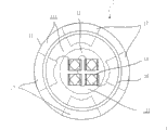
Fig. 1 is the top view according to the semiconductor luminous element packing structure of of the present invention one preferred specific embodiment.
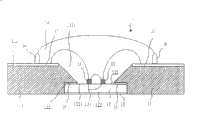
Fig. 2 is the cross section view according to the semiconductor luminous element packing structure of of the present invention one preferred specific embodiment.
Fig. 3 is the cross section view according to the semiconductor luminous element packing structure of the of the present invention second preferred specific embodiment.
Fig. 4 is the cross section view according to the semiconductor luminous element packing structure of the of the present invention the 3rd preferred specific embodiment.
The simple symbol explanation
1: encapsulating structure 11: substrate
12: lower bottom base 13: the semiconductor light emitting small pieces
14: encapsulating material 15: the heat conduction colloid
16: protuberance 17: outer electrode
111: top surface 112: basal surface
1121: the second depressed parts of 1111: the first depressed parts
121: first surface 122: second surface
131: the small pieces bottom
Embodiment
Main purpose of the present invention is to provide an encapsulating structure, and this encapsulating structure is applicable to various display device and lighting apparatus in order to encapsulate semiconductor light emitting component at least.Hereinafter will describe in detail according to an advantageous embodiment of the invention and execution mode.
See also Fig. 1.Fig. 1 is the top view according to the semiconductor luminous element packing structure 1 of of the present invention one preferred specific embodiment.This encapsulating structure 1 has a substrate 11, a lower bottom base 12 and at least one semiconductor light emitting small pieces 13, and this substrate 11 definition one top surface 111 is provided with a plurality of outer electrodes 17 on this top surface 111.This lower bottom base 12 definition one first surface 121, these at least one semiconductor light emitting small pieces 13 are fixed in this first surface 121 of this lower bottom base 12 by the internal electrode (bond pad) of its bottom (Bottom) 131.
See also Fig. 2.Fig. 2 is the cross section view according to the semiconductor luminous element packing structure 1 of of the present invention one preferred specific embodiment.This encapsulating structure 1 comprises a substrate 11, a lower bottom base 12, at least one semiconductor light emitting small pieces 13, and an encapsulating material 14, and wherein with similar elements part shown in Figure 1, preceding enumeration repeats no more.This top surface 111 of this substrate 11 forms one first depressed part 1111, also define a basal surface 112 on this substrate 11, this basal surface 112 of this substrate 11 forms one second depressed part 1121, this second depressed part 1121 is connected with first depressed part 1111, and this lower bottom base 12 is embedded in this second depressed part 1121, this lower bottom base 12 also defines a second surface 122, this first surface 121 of this lower bottom base 12 is exposed to the inside of this first depressed part 1111, and this top surface 111 forms a protuberance 16 along the edge of first depressed part 1111.These at least one semiconductor light emitting small pieces 13 have a bottom 131, and this first surface 121 that this lower bottom base 12 is fixed in this bottom 131 is exposed to the part of these first depressed part, 1111 inside.This encapsulating material 14 is used to fill the inside of this protuberance 16, in order to cover these at least one semiconductor light emitting small pieces 13.These at least one semiconductor light emitting small pieces 13 have internal electrode, and see through circuit and outer electrode 17 conductings (Electricallycoupled) that are positioned at this top surface 111.The internal electrode that at least one semiconductor light emitting small pieces 13 of this of present embodiment have is adapted to the kenel of connecting with the connected mode of outer electrode 17, but the connected mode of these electrodes also can adopt kenel in parallel to connect, and still can reach purpose of the present invention.
One heat conduction colloid 15 places between this bottom of this first surface 121 of this lower bottom base 12 and this first depressed part 1111, with in conjunction with this first surface 121 of this lower bottom base 12 and this bottom of this first depression 1111, that is in order to link this substrate 11 and this lower bottom base 12.
See also Fig. 3.Fig. 3 is the cross section view according to the semiconductor luminous element packing structure 1 of the of the present invention second preferred specific embodiment.Wherein with similar elements part shown in Figure 2, preceding enumeration repeats no more.This second surface 122 of this lower bottom base 12 constitutes a parallel surface with this basal surface 112 of this substrate 11, and further be coated with last layer heat-conducting glue body 15 in the below of this second surface 122 of this lower bottom base 12, to such an extent as to this basal surface 112 of this second surface 122 of this lower bottom base 12 and this substrate 11 constitutes a plane.
See also Fig. 4.Fig. 4 is the cross section view according to the semiconductor luminous element packing structure 1 of the of the present invention the 3rd preferred specific embodiment.Wherein with similar elements part shown in Figure 2, preceding enumeration repeats no more.This second surface 122 of this lower bottom base 12 constitutes a parallel surface with this basal surface 112 of this substrate 11, and further be coated with last layer heat-conducting glue body 15 in the below of this basal surface 112 of this substrate 11, to such an extent as to this basal surface 112 of this second surface 122 of this lower bottom base 12 and this substrate 11 constitutes a plane.
The invention provides the encapsulating structure of a tool high cooling efficiency, this encapsulating structure is in order to encapsulate semiconductor light emitting component at least, also can cooperate heat-transfer device further effectively to get rid of a large amount of heats that the high power semiconductor light-emitting component is produced, to solve conventional package structure and the radiating module too high problem of thermal resistance that the interface was had between the two.
By the detailed description of above preferred specific embodiment, hope can be known description feature of the present invention and spirit more, and is not to come category of the present invention is limited with above-mentioned disclosed preferred specific embodiment.On the contrary, its objective is that hope can contain in the category of claim of being arranged in of various changes and tool equality institute of the present invention desire application.
Claims (13)
1, a kind of semiconductor luminous element packing structure comprises:
One substrate, definition one top surface and a basal surface on this substrate form one first depressed part on this top surface of this substrate, form one second depressed part on this basal surface of this substrate, and this second depressed part is connected with this first depressed part, is provided with a plurality of outer electrodes on this top surface;
One lower bottom base engages with this second depressed part, this lower bottom base is a tabular, definition one first surface and a second surface on it, this lower bottom base is embedded in this second depressed part, to such an extent as to the part of this first surface of this lower bottom base is exposed to the inside of this first depressed part;
A plurality of semiconductor light emitting small pieces, wherein each semiconductor light emitting small pieces comprises a bottom and an internal electrode, these a plurality of semiconductor light emitting small pieces are electrically connected each other and are electrically connected with this substrate, and this first surface that these a plurality of semiconductor light emitting small pieces are fixed in this lower bottom base by this bottom is exposed to the part of this first depressed part inside; And
One encapsulating material, this encapsulating material are used to fill this first depressed part inside, to cover these a plurality of semiconductor light emitting small pieces.
2, semiconductor luminous element packing structure as claimed in claim 1, wherein the size of this first depressed part is less than the size of this second depressed part, to such an extent as to this first depressed part has a bottom, between this first surface that a heat conduction colloid places this lower bottom base and this bottom of this first depressed part with this first surface of combining this lower bottom base and this bottom of this first depressed part.
3, semiconductor luminous element packing structure as claimed in claim 1, wherein the edge along this first depressed part forms a protuberance on this top surface, this encapsulating material and be used to fill this protuberance inside.
4, semiconductor luminous element packing structure as claimed in claim 1, wherein this substrate is made of wherein a kind of institute of metal, pottery, flexible printed wiring board and rigid printed circuit board.
5, semiconductor luminous element packing structure as claimed in claim 1, wherein this lower bottom base is made up of semiconductor.
6, semiconductor luminous element packing structure as claimed in claim 1, wherein this basal surface of this second surface of this lower bottom base and this substrate constitutes a parallel surface.
7, semiconductor luminous element packing structure as claimed in claim 6, wherein this basal surface of this second surface of this lower bottom base and this substrate constitutes a plane.
8, semiconductor luminous element packing structure as claimed in claim 1, wherein these a plurality of semiconductor light emitting small pieces comprise a white light-emitting diodes.
9, semiconductor luminous element packing structure as claimed in claim 6, wherein these a plurality of semiconductor light emitting small pieces comprise a blue light diode.
10, semiconductor luminous element packing structure as claimed in claim 1, wherein these a plurality of semiconductor light emitting small pieces comprise at least one red diodes, at least one blue light diode and at least one green diode.
11, semiconductor luminous element packing structure as claimed in claim 1, wherein this lower bottom base is made by semiconductor, and this semiconductor is provided with circuit and is electrically connected with these a plurality of semiconductor light emitting small pieces.
12, semiconductor luminous element packing structure as claimed in claim 1 wherein scribbles the heat conduction colloid on this second surface of this lower bottom base, makes this second surface of this lower bottom base and this basal surface of this substrate constitute a plane.
13, semiconductor luminous element packing structure as claimed in claim 1, wherein this basal surface of this substrate scribbles the heat conduction colloid, makes this second surface of this lower bottom base and this basal surface of this substrate constitute a plane.
Priority Applications (8)
| Application Number | Priority Date | Filing Date | Title |
|---|---|---|---|
| CNB2005100747311A CN100435361C (en) | 2005-05-31 | 2005-05-31 | Semiconductor luminous element packing structure |
| US11/921,176 US7777237B2 (en) | 2005-05-31 | 2006-05-31 | Semiconductor light-emitting device and method of fabricating the same |
| JP2008513899A JP5043832B2 (en) | 2005-05-31 | 2006-05-31 | Semiconductor light emitting device and manufacturing method thereof |
| EP06742052.1A EP1898473A4 (en) | 2005-05-31 | 2006-05-31 | Package structure of semiconductor light-emitting device |
| PCT/CN2006/001165 WO2006128375A1 (en) | 2005-05-31 | 2006-05-31 | Package structure of semiconductor light-emitting device |
| KR1020077030972A KR20080030584A (en) | 2005-05-31 | 2006-05-31 | Package structure of semiconductor light-emitting device |
| AU2006254610A AU2006254610B2 (en) | 2005-05-31 | 2006-05-31 | Package structure of semiconductor light-emitting device |
| US12/834,082 US7985973B2 (en) | 2005-05-31 | 2010-07-12 | Semiconductor light-emitting device and method of fabricating the same |
Applications Claiming Priority (1)
| Application Number | Priority Date | Filing Date | Title |
|---|---|---|---|
| CNB2005100747311A CN100435361C (en) | 2005-05-31 | 2005-05-31 | Semiconductor luminous element packing structure |
Publications (2)
| Publication Number | Publication Date |
|---|---|
| CN1874014A CN1874014A (en) | 2006-12-06 |
| CN100435361C true CN100435361C (en) | 2008-11-19 |
Family
ID=37481232
Family Applications (1)
| Application Number | Title | Priority Date | Filing Date |
|---|---|---|---|
| CNB2005100747311A Expired - Fee Related CN100435361C (en) | 2005-05-31 | 2005-05-31 | Semiconductor luminous element packing structure |
Country Status (7)
| Country | Link |
|---|---|
| US (2) | US7777237B2 (en) |
| EP (1) | EP1898473A4 (en) |
| JP (1) | JP5043832B2 (en) |
| KR (1) | KR20080030584A (en) |
| CN (1) | CN100435361C (en) |
| AU (1) | AU2006254610B2 (en) |
| WO (1) | WO2006128375A1 (en) |
Families Citing this family (22)
| Publication number | Priority date | Publication date | Assignee | Title |
|---|---|---|---|---|
| US7786490B2 (en) * | 2005-11-28 | 2010-08-31 | Neobule Technologies, Inc. | Multi-chip module single package structure for semiconductor |
| US20100181590A1 (en) * | 2007-06-25 | 2010-07-22 | Jen-Shyan Chen | Light-emitting diode illuminating apparatus |
| WO2009000105A1 (en) * | 2007-06-25 | 2008-12-31 | Jenshyan Chen | A light-emitting diode lighting device |
| WO2009000104A1 (en) * | 2007-06-25 | 2008-12-31 | Jenshyan Chen | The package structure of led |
| JP5320560B2 (en) | 2008-05-20 | 2013-10-23 | 東芝ライテック株式会社 | Light source unit and lighting device |
| KR101039496B1 (en) * | 2008-06-17 | 2011-06-08 | 한국광기술원 | Light emitting diode package having dome type encapsulation layer and method for fabricating the same |
| KR101465161B1 (en) * | 2008-09-04 | 2014-11-25 | 삼성전자주식회사 | semiconductor package and method for manufacturing the same |
| KR101018119B1 (en) | 2008-09-04 | 2011-02-25 | 삼성엘이디 주식회사 | LED package |
| KR101018183B1 (en) * | 2008-10-15 | 2011-02-28 | 삼성엘이디 주식회사 | White Light emitting device package |
| KR101038808B1 (en) * | 2008-12-11 | 2011-06-03 | 삼성엘이디 주식회사 | Ac driven white light emitting device |
| KR100981651B1 (en) * | 2008-12-26 | 2010-09-10 | 김민공 | Lens protected chip led package |
| RU2488195C2 (en) * | 2009-03-10 | 2013-07-20 | Непес Лед Корпорейшн | Assembly of light-emitting diode (led) lead-frame unit, led group using this lead-frame and method for manufacturing of led group |
| KR101144146B1 (en) * | 2009-04-15 | 2012-05-09 | (주)웨이브닉스이에스피 | Photonic Device Package Module and Process of The Same |
| DE102009054474A1 (en) * | 2009-12-10 | 2011-06-16 | Osram Gesellschaft mit beschränkter Haftung | Light module and light chain |
| KR101144741B1 (en) * | 2010-03-30 | 2012-05-24 | 주식회사 엠디티 | Package for light emitting diode |
| KR101147614B1 (en) * | 2010-06-16 | 2012-05-23 | 솔레즈 주식회사 | Light Emitting Diode Chip Package |
| US20110316417A1 (en) * | 2010-06-25 | 2011-12-29 | Jen-Shyan Chen | Light-emitting diode illumination platform |
| US8967887B2 (en) * | 2011-05-20 | 2015-03-03 | Tyco Electronics Corporation | Environmentally-sealable package for optical assembly |
| TWI598665B (en) * | 2013-03-15 | 2017-09-11 | 隆達電子股份有限公司 | Luminous element, bar-type luminous element and applications thereof |
| TWI549322B (en) * | 2013-04-10 | 2016-09-11 | 映瑞光電科技(上海)有限公司 | Led component by integrating epitaxial structure and package substrate together and method of manufacturing the same |
| US10164159B2 (en) | 2016-12-20 | 2018-12-25 | Samsung Electronics Co., Ltd. | Light-emitting diode package and method of manufacturing the same |
| JP7231809B2 (en) * | 2018-06-05 | 2023-03-02 | 日亜化学工業株式会社 | light emitting device |
Citations (4)
| Publication number | Priority date | Publication date | Assignee | Title |
|---|---|---|---|---|
| CN1436374A (en) * | 2001-04-12 | 2003-08-13 | 松下电工株式会社 | Light source device using LED, and method of producing same |
| CN1466782A (en) * | 2001-08-28 | 2004-01-07 | ���µ繤��ʽ���� | Loghting device using LED |
| US20040124487A1 (en) * | 2002-12-06 | 2004-07-01 | Loh Ban P. | LED package die having a small footprint |
| CN1538538A (en) * | 2003-04-09 | 2004-10-20 | �����ǵ��ӹɷ�����˾ | LED lamp |
Family Cites Families (12)
| Publication number | Priority date | Publication date | Assignee | Title |
|---|---|---|---|---|
| JP3431038B2 (en) * | 1994-02-18 | 2003-07-28 | ローム株式会社 | LIGHT EMITTING DEVICE, ITS MANUFACTURING METHOD, AND LED HEAD MANUFACTURING METHOD |
| JPH10144963A (en) * | 1996-11-05 | 1998-05-29 | Sanyo Electric Co Ltd | Led light source and its manufacture |
| US6489637B1 (en) * | 1999-06-09 | 2002-12-03 | Sanyo Electric Co., Ltd. | Hybrid integrated circuit device |
| JP3406270B2 (en) * | 2000-02-17 | 2003-05-12 | 沖電気工業株式会社 | Semiconductor device and manufacturing method thereof |
| JP2003046135A (en) * | 2001-07-27 | 2003-02-14 | Matsushita Electric Ind Co Ltd | Semiconductor light emitting device |
| CN2612075Y (en) * | 2003-02-08 | 2004-04-14 | 光鼎电子股份有限公司 | Package structure for LED |
| JP2004260048A (en) * | 2003-02-27 | 2004-09-16 | Korai Kagi Kofun Yugenkoshi | Micro-type light emitting device |
| US6835960B2 (en) | 2003-03-03 | 2004-12-28 | Opto Tech Corporation | Light emitting diode package structure |
| DE102004034166B4 (en) * | 2003-07-17 | 2015-08-20 | Toyoda Gosei Co., Ltd. | Light-emitting device |
| TWM261835U (en) * | 2004-07-22 | 2005-04-11 | Everlight Electronics Co Ltd | High power LED assembly structure |
| JP2006060070A (en) * | 2004-08-20 | 2006-03-02 | Kyoritsu Elex Co Ltd | Light-emitting diode, package therefor, and method for manufacturing the package |
| JP2006128511A (en) * | 2004-10-29 | 2006-05-18 | Ngk Spark Plug Co Ltd | Ceramic substrate for light emitting element |
-
2005
- 2005-05-31 CN CNB2005100747311A patent/CN100435361C/en not_active Expired - Fee Related
-
2006
- 2006-05-31 WO PCT/CN2006/001165 patent/WO2006128375A1/en active Application Filing
- 2006-05-31 AU AU2006254610A patent/AU2006254610B2/en not_active Ceased
- 2006-05-31 KR KR1020077030972A patent/KR20080030584A/en not_active Application Discontinuation
- 2006-05-31 EP EP06742052.1A patent/EP1898473A4/en not_active Withdrawn
- 2006-05-31 US US11/921,176 patent/US7777237B2/en not_active Expired - Fee Related
- 2006-05-31 JP JP2008513899A patent/JP5043832B2/en not_active Expired - Fee Related
-
2010
- 2010-07-12 US US12/834,082 patent/US7985973B2/en not_active Expired - Fee Related
Patent Citations (4)
| Publication number | Priority date | Publication date | Assignee | Title |
|---|---|---|---|---|
| CN1436374A (en) * | 2001-04-12 | 2003-08-13 | 松下电工株式会社 | Light source device using LED, and method of producing same |
| CN1466782A (en) * | 2001-08-28 | 2004-01-07 | ���µ繤��ʽ���� | Loghting device using LED |
| US20040124487A1 (en) * | 2002-12-06 | 2004-07-01 | Loh Ban P. | LED package die having a small footprint |
| CN1538538A (en) * | 2003-04-09 | 2004-10-20 | �����ǵ��ӹɷ�����˾ | LED lamp |
Also Published As
| Publication number | Publication date |
|---|---|
| JP2008543064A (en) | 2008-11-27 |
| US7985973B2 (en) | 2011-07-26 |
| CN1874014A (en) | 2006-12-06 |
| EP1898473A4 (en) | 2013-11-20 |
| US20100270565A1 (en) | 2010-10-28 |
| AU2006254610B2 (en) | 2011-09-08 |
| EP1898473A1 (en) | 2008-03-12 |
| US7777237B2 (en) | 2010-08-17 |
| AU2006254610A1 (en) | 2006-12-07 |
| US20090101932A1 (en) | 2009-04-23 |
| JP5043832B2 (en) | 2012-10-10 |
| KR20080030584A (en) | 2008-04-04 |
| WO2006128375A1 (en) | 2006-12-07 |
Similar Documents
| Publication | Publication Date | Title |
|---|---|---|
| CN100435361C (en) | Semiconductor luminous element packing structure | |
| CN101603677B (en) | LED lamp fitting | |
| CN201868429U (en) | Embedded-type encapsulating structure of luminous diode | |
| CN102064247A (en) | Packaging method and packaging structure for embedded light emitting diode | |
| CN203150541U (en) | LED light source based on COB packaging | |
| CN202839748U (en) | White light source module based on flip LED chips | |
| CN103470968A (en) | Light emitting diode lamp core with large light emitting angle and illumination device with lamp core | |
| CN203309586U (en) | LED (Light Emitting Diode) light source module based on printed circuit board | |
| CN201428943Y (en) | Led lamp | |
| CN208011317U (en) | Side entering type LED light source for LED light | |
| CN100414728C (en) | White light LED package radiating structure | |
| CN103307483A (en) | LED light source module based on printed circuit board | |
| WO2009082864A1 (en) | A led light source with the shape of a bar | |
| CN105953103A (en) | LED non-planar heat-dissipating PCB bulb and processing technology thereof | |
| CN202532237U (en) | Dustproof LED (Light Emitting Diode) module easily radiating heat | |
| CN202384336U (en) | Light-emitting diode (LED) light source module | |
| CN201103878Y (en) | LED light source and lamp using the same | |
| CN202259437U (en) | Multi-reflection cup integrated type LED (light emitting diode) packaging structure | |
| CN2798315Y (en) | High power LED packing structure | |
| CN200983368Y (en) | High heat radiation package base plate of high brightness LED | |
| CN203707166U (en) | All-metal integrated LED lamp bead packaging structure | |
| CN201078685Y (en) | Light emitting diode light source and light fitting using the same | |
| CN202259288U (en) | LED substrate structure | |
| CN210040256U (en) | High heat dissipation LED base plate | |
| CN202948978U (en) | White-light light-emitting diode (LED) apparatus with cubic boron nitride film for promoting cooling of chips |
Legal Events
| Date | Code | Title | Description |
|---|---|---|---|
| C06 | Publication | ||
| PB01 | Publication | ||
| C10 | Entry into substantive examination | ||
| SE01 | Entry into force of request for substantive examination | ||
| C14 | Grant of patent or utility model | ||
| GR01 | Patent grant | ||
| C41 | Transfer of patent application or patent right or utility model | ||
| TR01 | Transfer of patent right |
Effective date of registration: 20160516 Address after: 201306 Shanghai Xinyuan Lingang Industrial District Road No. 555 financial center room 211 Patentee after: EnRay Tek Optoelectronics (Shanghai) Co., Ltd. Address before: Brunei Darussalam Bandar Seri Begawan Patentee before: New Light Source Technology Co., Ltd. |
|
| CF01 | Termination of patent right due to non-payment of annual fee | ||
| CF01 | Termination of patent right due to non-payment of annual fee |
Granted publication date: 20081119 Termination date: 20200531 |