EP2592664B1 - A vertical-topology semiconductor light-emitting device - Google Patents
A vertical-topology semiconductor light-emitting device Download PDFInfo
- Publication number
- EP2592664B1 EP2592664B1 EP13154098.1A EP13154098A EP2592664B1 EP 2592664 B1 EP2592664 B1 EP 2592664B1 EP 13154098 A EP13154098 A EP 13154098A EP 2592664 B1 EP2592664 B1 EP 2592664B1
- Authority
- EP
- European Patent Office
- Prior art keywords
- layer
- gan
- emitting device
- light emitting
- vertical topology
- Prior art date
- Legal status (The legal status is an assumption and is not a legal conclusion. Google has not performed a legal analysis and makes no representation as to the accuracy of the status listed.)
- Expired - Lifetime
Links
- 239000004065 semiconductor Substances 0.000 title claims description 60
- 239000010410 layer Substances 0.000 claims description 144
- 229910052751 metal Inorganic materials 0.000 claims description 56
- 239000002184 metal Substances 0.000 claims description 56
- 229910052737 gold Inorganic materials 0.000 claims description 16
- 229910052782 aluminium Inorganic materials 0.000 claims description 11
- 229910052802 copper Inorganic materials 0.000 claims description 8
- 239000010936 titanium Substances 0.000 claims description 7
- 239000011229 interlayer Substances 0.000 claims description 4
- 229910052763 palladium Inorganic materials 0.000 claims description 4
- RTAQQCXQSZGOHL-UHFFFAOYSA-N Titanium Chemical compound [Ti] RTAQQCXQSZGOHL-UHFFFAOYSA-N 0.000 claims description 3
- XAGFODPZIPBFFR-UHFFFAOYSA-N aluminium Chemical compound [Al] XAGFODPZIPBFFR-UHFFFAOYSA-N 0.000 claims description 3
- 229910052804 chromium Inorganic materials 0.000 claims description 3
- 229910052697 platinum Inorganic materials 0.000 claims description 3
- 229910052719 titanium Inorganic materials 0.000 claims description 3
- 229910002601 GaN Inorganic materials 0.000 description 95
- 239000000758 substrate Substances 0.000 description 85
- JMASRVWKEDWRBT-UHFFFAOYSA-N Gallium nitride Chemical compound [Ga]#N JMASRVWKEDWRBT-UHFFFAOYSA-N 0.000 description 81
- 229910052594 sapphire Inorganic materials 0.000 description 58
- 239000010980 sapphire Substances 0.000 description 58
- 238000000034 method Methods 0.000 description 42
- 239000010408 film Substances 0.000 description 35
- 235000012431 wafers Nutrition 0.000 description 31
- 238000004519 manufacturing process Methods 0.000 description 18
- 239000000463 material Substances 0.000 description 12
- 238000005530 etching Methods 0.000 description 11
- 238000001020 plasma etching Methods 0.000 description 10
- 238000005498 polishing Methods 0.000 description 8
- 230000009286 beneficial effect Effects 0.000 description 7
- 230000003287 optical effect Effects 0.000 description 7
- 230000015572 biosynthetic process Effects 0.000 description 6
- 229920006332 epoxy adhesive Polymers 0.000 description 6
- 230000012010 growth Effects 0.000 description 6
- 238000009616 inductively coupled plasma Methods 0.000 description 6
- 238000001312 dry etching Methods 0.000 description 5
- 238000001039 wet etching Methods 0.000 description 5
- 238000010438 heat treatment Methods 0.000 description 4
- 239000000203 mixture Substances 0.000 description 4
- 238000000926 separation method Methods 0.000 description 4
- XUIMIQQOPSSXEZ-UHFFFAOYSA-N Silicon Chemical compound [Si] XUIMIQQOPSSXEZ-UHFFFAOYSA-N 0.000 description 3
- 230000008901 benefit Effects 0.000 description 3
- MVPPADPHJFYWMZ-UHFFFAOYSA-N chlorobenzene Chemical compound ClC1=CC=CC=C1 MVPPADPHJFYWMZ-UHFFFAOYSA-N 0.000 description 3
- 239000011248 coating agent Substances 0.000 description 3
- 238000000576 coating method Methods 0.000 description 3
- 238000007772 electroless plating Methods 0.000 description 3
- 238000009713 electroplating Methods 0.000 description 3
- 239000007789 gas Substances 0.000 description 3
- 150000002500 ions Chemical class 0.000 description 3
- 229910052759 nickel Inorganic materials 0.000 description 3
- 230000001681 protective effect Effects 0.000 description 3
- 229910052710 silicon Inorganic materials 0.000 description 3
- 239000010703 silicon Substances 0.000 description 3
- 239000010409 thin film Substances 0.000 description 3
- CSCPPACGZOOCGX-UHFFFAOYSA-N Acetone Chemical compound CC(C)=O CSCPPACGZOOCGX-UHFFFAOYSA-N 0.000 description 2
- QAOWNCQODCNURD-UHFFFAOYSA-N Sulfuric acid Chemical compound OS(O)(=O)=O QAOWNCQODCNURD-UHFFFAOYSA-N 0.000 description 2
- 238000010521 absorption reaction Methods 0.000 description 2
- QZPSXPBJTPJTSZ-UHFFFAOYSA-N aqua regia Chemical compound Cl.O[N+]([O-])=O QZPSXPBJTPJTSZ-UHFFFAOYSA-N 0.000 description 2
- 238000004140 cleaning Methods 0.000 description 2
- 238000005520 cutting process Methods 0.000 description 2
- 238000000151 deposition Methods 0.000 description 2
- 238000011982 device technology Methods 0.000 description 2
- AMGQUBHHOARCQH-UHFFFAOYSA-N indium;oxotin Chemical compound [In].[Sn]=O AMGQUBHHOARCQH-UHFFFAOYSA-N 0.000 description 2
- 238000001451 molecular beam epitaxy Methods 0.000 description 2
- 230000007935 neutral effect Effects 0.000 description 2
- 238000005240 physical vapour deposition Methods 0.000 description 2
- 239000000243 solution Substances 0.000 description 2
- 239000000126 substance Substances 0.000 description 2
- 238000006467 substitution reaction Methods 0.000 description 2
- 229910015844 BCl3 Inorganic materials 0.000 description 1
- PNEYBMLMFCGWSK-UHFFFAOYSA-N aluminium oxide Inorganic materials [O-2].[O-2].[O-2].[Al+3].[Al+3] PNEYBMLMFCGWSK-UHFFFAOYSA-N 0.000 description 1
- 238000005234 chemical deposition Methods 0.000 description 1
- 238000005229 chemical vapour deposition Methods 0.000 description 1
- 229910052593 corundum Inorganic materials 0.000 description 1
- 239000013078 crystal Substances 0.000 description 1
- 230000008021 deposition Effects 0.000 description 1
- 239000010432 diamond Substances 0.000 description 1
- 229910003460 diamond Inorganic materials 0.000 description 1
- 238000007598 dipping method Methods 0.000 description 1
- 239000002019 doping agent Substances 0.000 description 1
- 230000005611 electricity Effects 0.000 description 1
- 239000007772 electrode material Substances 0.000 description 1
- 230000005672 electromagnetic field Effects 0.000 description 1
- 238000000227 grinding Methods 0.000 description 1
- 230000017525 heat dissipation Effects 0.000 description 1
- 229910052738 indium Inorganic materials 0.000 description 1
- APFVFJFRJDLVQX-UHFFFAOYSA-N indium atom Chemical compound [In] APFVFJFRJDLVQX-UHFFFAOYSA-N 0.000 description 1
- 230000001939 inductive effect Effects 0.000 description 1
- 238000002347 injection Methods 0.000 description 1
- 239000007924 injection Substances 0.000 description 1
- 239000012212 insulator Substances 0.000 description 1
- 238000001459 lithography Methods 0.000 description 1
- 230000008018 melting Effects 0.000 description 1
- 238000002844 melting Methods 0.000 description 1
- 229910044991 metal oxide Inorganic materials 0.000 description 1
- 150000004706 metal oxides Chemical class 0.000 description 1
- 230000005693 optoelectronics Effects 0.000 description 1
- TWNQGVIAIRXVLR-UHFFFAOYSA-N oxo(oxoalumanyloxy)alumane Chemical compound O=[Al]O[Al]=O TWNQGVIAIRXVLR-UHFFFAOYSA-N 0.000 description 1
- 239000002245 particle Substances 0.000 description 1
- 238000005289 physical deposition Methods 0.000 description 1
- 239000010453 quartz Substances 0.000 description 1
- 238000002310 reflectometry Methods 0.000 description 1
- 238000005096 rolling process Methods 0.000 description 1
- 238000007788 roughening Methods 0.000 description 1
- 238000005488 sandblasting Methods 0.000 description 1
- 238000005389 semiconductor device fabrication Methods 0.000 description 1
- VYPSYNLAJGMNEJ-UHFFFAOYSA-N silicon dioxide Inorganic materials O=[Si]=O VYPSYNLAJGMNEJ-UHFFFAOYSA-N 0.000 description 1
- 238000003892 spreading Methods 0.000 description 1
- 230000003068 static effect Effects 0.000 description 1
- 230000002459 sustained effect Effects 0.000 description 1
- FAQYAMRNWDIXMY-UHFFFAOYSA-N trichloroborane Chemical compound ClB(Cl)Cl FAQYAMRNWDIXMY-UHFFFAOYSA-N 0.000 description 1
- 238000000927 vapour-phase epitaxy Methods 0.000 description 1
- 229910001845 yogo sapphire Inorganic materials 0.000 description 1
Images


Classifications
-
- H—ELECTRICITY
- H01—ELECTRIC ELEMENTS
- H01L—SEMICONDUCTOR DEVICES NOT COVERED BY CLASS H10
- H01L33/00—Semiconductor devices having potential barriers specially adapted for light emission; Processes or apparatus specially adapted for the manufacture or treatment thereof or of parts thereof; Details thereof
- H01L33/02—Semiconductor devices having potential barriers specially adapted for light emission; Processes or apparatus specially adapted for the manufacture or treatment thereof or of parts thereof; Details thereof characterised by the semiconductor bodies
- H01L33/26—Materials of the light emitting region
- H01L33/30—Materials of the light emitting region containing only elements of Group III and Group V of the Periodic Table
- H01L33/32—Materials of the light emitting region containing only elements of Group III and Group V of the Periodic Table containing nitrogen
-
- H—ELECTRICITY
- H01—ELECTRIC ELEMENTS
- H01L—SEMICONDUCTOR DEVICES NOT COVERED BY CLASS H10
- H01L33/00—Semiconductor devices having potential barriers specially adapted for light emission; Processes or apparatus specially adapted for the manufacture or treatment thereof or of parts thereof; Details thereof
- H01L33/005—Processes
- H01L33/0093—Wafer bonding; Removal of the growth substrate
-
- H—ELECTRICITY
- H01—ELECTRIC ELEMENTS
- H01L—SEMICONDUCTOR DEVICES NOT COVERED BY CLASS H10
- H01L33/00—Semiconductor devices having potential barriers specially adapted for light emission; Processes or apparatus specially adapted for the manufacture or treatment thereof or of parts thereof; Details thereof
- H01L33/02—Semiconductor devices having potential barriers specially adapted for light emission; Processes or apparatus specially adapted for the manufacture or treatment thereof or of parts thereof; Details thereof characterised by the semiconductor bodies
- H01L33/04—Semiconductor devices having potential barriers specially adapted for light emission; Processes or apparatus specially adapted for the manufacture or treatment thereof or of parts thereof; Details thereof characterised by the semiconductor bodies with a quantum effect structure or superlattice, e.g. tunnel junction
-
- H—ELECTRICITY
- H01—ELECTRIC ELEMENTS
- H01L—SEMICONDUCTOR DEVICES NOT COVERED BY CLASS H10
- H01L33/00—Semiconductor devices having potential barriers specially adapted for light emission; Processes or apparatus specially adapted for the manufacture or treatment thereof or of parts thereof; Details thereof
- H01L33/02—Semiconductor devices having potential barriers specially adapted for light emission; Processes or apparatus specially adapted for the manufacture or treatment thereof or of parts thereof; Details thereof characterised by the semiconductor bodies
- H01L33/14—Semiconductor devices having potential barriers specially adapted for light emission; Processes or apparatus specially adapted for the manufacture or treatment thereof or of parts thereof; Details thereof characterised by the semiconductor bodies with a carrier transport control structure, e.g. highly-doped semiconductor layer or current-blocking structure
-
- H—ELECTRICITY
- H01—ELECTRIC ELEMENTS
- H01L—SEMICONDUCTOR DEVICES NOT COVERED BY CLASS H10
- H01L33/00—Semiconductor devices having potential barriers specially adapted for light emission; Processes or apparatus specially adapted for the manufacture or treatment thereof or of parts thereof; Details thereof
- H01L33/36—Semiconductor devices having potential barriers specially adapted for light emission; Processes or apparatus specially adapted for the manufacture or treatment thereof or of parts thereof; Details thereof characterised by the electrodes
- H01L33/40—Materials therefor
- H01L33/405—Reflective materials
-
- H—ELECTRICITY
- H01—ELECTRIC ELEMENTS
- H01L—SEMICONDUCTOR DEVICES NOT COVERED BY CLASS H10
- H01L33/00—Semiconductor devices having potential barriers specially adapted for light emission; Processes or apparatus specially adapted for the manufacture or treatment thereof or of parts thereof; Details thereof
- H01L33/44—Semiconductor devices having potential barriers specially adapted for light emission; Processes or apparatus specially adapted for the manufacture or treatment thereof or of parts thereof; Details thereof characterised by the coatings, e.g. passivation layer or anti-reflective coating
- H01L33/46—Reflective coating, e.g. dielectric Bragg reflector
-
- H—ELECTRICITY
- H01—ELECTRIC ELEMENTS
- H01L—SEMICONDUCTOR DEVICES NOT COVERED BY CLASS H10
- H01L33/00—Semiconductor devices having potential barriers specially adapted for light emission; Processes or apparatus specially adapted for the manufacture or treatment thereof or of parts thereof; Details thereof
- H01L33/48—Semiconductor devices having potential barriers specially adapted for light emission; Processes or apparatus specially adapted for the manufacture or treatment thereof or of parts thereof; Details thereof characterised by the semiconductor body packages
- H01L33/52—Encapsulations
- H01L33/54—Encapsulations having a particular shape
-
- H—ELECTRICITY
- H01—ELECTRIC ELEMENTS
- H01L—SEMICONDUCTOR DEVICES NOT COVERED BY CLASS H10
- H01L33/00—Semiconductor devices having potential barriers specially adapted for light emission; Processes or apparatus specially adapted for the manufacture or treatment thereof or of parts thereof; Details thereof
- H01L33/48—Semiconductor devices having potential barriers specially adapted for light emission; Processes or apparatus specially adapted for the manufacture or treatment thereof or of parts thereof; Details thereof characterised by the semiconductor body packages
- H01L33/58—Optical field-shaping elements
- H01L33/60—Reflective elements
-
- H—ELECTRICITY
- H01—ELECTRIC ELEMENTS
- H01L—SEMICONDUCTOR DEVICES NOT COVERED BY CLASS H10
- H01L33/00—Semiconductor devices having potential barriers specially adapted for light emission; Processes or apparatus specially adapted for the manufacture or treatment thereof or of parts thereof; Details thereof
- H01L33/48—Semiconductor devices having potential barriers specially adapted for light emission; Processes or apparatus specially adapted for the manufacture or treatment thereof or of parts thereof; Details thereof characterised by the semiconductor body packages
- H01L33/62—Arrangements for conducting electric current to or from the semiconductor body, e.g. lead-frames, wire-bonds or solder balls
-
- H—ELECTRICITY
- H01—ELECTRIC ELEMENTS
- H01L—SEMICONDUCTOR DEVICES NOT COVERED BY CLASS H10
- H01L33/00—Semiconductor devices having potential barriers specially adapted for light emission; Processes or apparatus specially adapted for the manufacture or treatment thereof or of parts thereof; Details thereof
- H01L33/48—Semiconductor devices having potential barriers specially adapted for light emission; Processes or apparatus specially adapted for the manufacture or treatment thereof or of parts thereof; Details thereof characterised by the semiconductor body packages
- H01L33/64—Heat extraction or cooling elements
- H01L33/647—Heat extraction or cooling elements the elements conducting electric current to or from the semiconductor body
-
- H—ELECTRICITY
- H01—ELECTRIC ELEMENTS
- H01L—SEMICONDUCTOR DEVICES NOT COVERED BY CLASS H10
- H01L33/00—Semiconductor devices having potential barriers specially adapted for light emission; Processes or apparatus specially adapted for the manufacture or treatment thereof or of parts thereof; Details thereof
- H01L33/005—Processes
- H01L33/0062—Processes for devices with an active region comprising only III-V compounds
- H01L33/0066—Processes for devices with an active region comprising only III-V compounds with a substrate not being a III-V compound
- H01L33/007—Processes for devices with an active region comprising only III-V compounds with a substrate not being a III-V compound comprising nitride compounds
-
- H—ELECTRICITY
- H01—ELECTRIC ELEMENTS
- H01L—SEMICONDUCTOR DEVICES NOT COVERED BY CLASS H10
- H01L33/00—Semiconductor devices having potential barriers specially adapted for light emission; Processes or apparatus specially adapted for the manufacture or treatment thereof or of parts thereof; Details thereof
- H01L33/005—Processes
- H01L33/0095—Post-treatment of devices, e.g. annealing, recrystallisation or short-circuit elimination
-
- H—ELECTRICITY
- H01—ELECTRIC ELEMENTS
- H01L—SEMICONDUCTOR DEVICES NOT COVERED BY CLASS H10
- H01L33/00—Semiconductor devices having potential barriers specially adapted for light emission; Processes or apparatus specially adapted for the manufacture or treatment thereof or of parts thereof; Details thereof
- H01L33/02—Semiconductor devices having potential barriers specially adapted for light emission; Processes or apparatus specially adapted for the manufacture or treatment thereof or of parts thereof; Details thereof characterised by the semiconductor bodies
- H01L33/12—Semiconductor devices having potential barriers specially adapted for light emission; Processes or apparatus specially adapted for the manufacture or treatment thereof or of parts thereof; Details thereof characterised by the semiconductor bodies with a stress relaxation structure, e.g. buffer layer
-
- H—ELECTRICITY
- H01—ELECTRIC ELEMENTS
- H01L—SEMICONDUCTOR DEVICES NOT COVERED BY CLASS H10
- H01L33/00—Semiconductor devices having potential barriers specially adapted for light emission; Processes or apparatus specially adapted for the manufacture or treatment thereof or of parts thereof; Details thereof
- H01L33/36—Semiconductor devices having potential barriers specially adapted for light emission; Processes or apparatus specially adapted for the manufacture or treatment thereof or of parts thereof; Details thereof characterised by the electrodes
- H01L33/38—Semiconductor devices having potential barriers specially adapted for light emission; Processes or apparatus specially adapted for the manufacture or treatment thereof or of parts thereof; Details thereof characterised by the electrodes with a particular shape
-
- H—ELECTRICITY
- H01—ELECTRIC ELEMENTS
- H01L—SEMICONDUCTOR DEVICES NOT COVERED BY CLASS H10
- H01L33/00—Semiconductor devices having potential barriers specially adapted for light emission; Processes or apparatus specially adapted for the manufacture or treatment thereof or of parts thereof; Details thereof
- H01L33/36—Semiconductor devices having potential barriers specially adapted for light emission; Processes or apparatus specially adapted for the manufacture or treatment thereof or of parts thereof; Details thereof characterised by the electrodes
- H01L33/40—Materials therefor
- H01L33/42—Transparent materials
-
- H—ELECTRICITY
- H01—ELECTRIC ELEMENTS
- H01L—SEMICONDUCTOR DEVICES NOT COVERED BY CLASS H10
- H01L33/00—Semiconductor devices having potential barriers specially adapted for light emission; Processes or apparatus specially adapted for the manufacture or treatment thereof or of parts thereof; Details thereof
- H01L33/48—Semiconductor devices having potential barriers specially adapted for light emission; Processes or apparatus specially adapted for the manufacture or treatment thereof or of parts thereof; Details thereof characterised by the semiconductor body packages
- H01L33/64—Heat extraction or cooling elements
- H01L33/641—Heat extraction or cooling elements characterized by the materials
Definitions
- the present invention relates to semiconductor device fabrication. More particularly, the present invention relates to a method of fabricating vertical devices using a metal support film.
- LEDs Light emitting diodes
- the color of the light (wavelength) that is emitted by an LED depends on the semiconductor material that is used to fabricate the LED. This is because the wavelength of the emitted light depends on the semiconductor material's band-gap energy, which represents the energy difference between valence band and conduction band electrons.
- GaN Gallium-Nitride
- InGaN/GaN semiconductor layers that emit green, blue, and white visible light.
- This wavelength control ability enables an LED semiconductor designer to tailor material characteristics to achieve beneficial device characteristics. For example, GaN enables an LED semiconductor designer to produce blue LEDs and blue laser diodes, which are beneficial in full color displays and in optical recordings, and white LEDs, which can replace incandescent lamps.
- GaN-based LEDs Because of the foregoing and other advantageous, the market for GaN-based LEDs is rapidly growing. Accordingly, GaN-based opto-electronic device technology has rapidly evolved since their commercial introduction in 1994. Because the efficiency of GaN light emitting diodes has surpassed that of incandescent lighting, and is now comparable with that of fluorescent lighting, the market for GaN based LEDs is expected to continue its rapid growth.
- GaN devices are too expensive for many applications.
- One reason for this is the high cost of manufacturing GaN-based devices, which in turn is related to the difficulties of growing GaN epitaxial layers and of subsequently dicing out completed GaN-based devices.
- GaN-based devices are typically fabricated on sapphire substrates. This is because sapphire wafers are commercially available in dimensions that are suitable for mass-producing GaN-based devices, because sapphire supports high-quality GaN epitaxial layer growths, and because of the extensive temperature handling capability of sapphire. Typically, GaN-based devices are fabricated on 2" diameter sapphire wafers that are either 330 or 430 microns thick. Such a diameter enables the fabrication of thousands of individual devices, while the thickness is sufficient to support device fabrication without excessive wafer warping. Furthermore, the sapphire crystal is chemically and thermally stable, has a high melting temperature that enables high temperature fabrication processes, has a high bonding energy (122.4 Kcal/mole), and a high dielectric constant. Chemically, sapphires are crystalline aluminum oxide, Al 2 O 3 .
- Fabricating semiconductor devices on sapphire is typically performed by growing an n-GaN epitaxial layer on a sapphire substrate using metal oxide chemical vapor deposition (MOCVD) or molecular beam epitaxy (MBE). Then, a plurality of individual devices, such as GaN LEDs, is fabricated on the epitaxial layer using normal semiconductor processing techniques. After the individual devices are fabricated they must be diced out of the sapphire substrate. However, since sapphires are extremely hard, are chemically resistant, and do not have natural cleave angles, sapphire substrates are difficult to dice. Indeed, dicing typically requires that the sapphire substrate be thinned to about 100 microns by mechanical grinding, lapping, and/or polishing.
- MOCVD metal oxide chemical vapor deposition
- MBE molecular beam epitaxy
- sapphire substrates or other insulating substrate have other drawbacks.
- sapphire is an insulator
- the device topologies that are available when using sapphire substrates (or other insulating substrates) are limited.
- lateral and vertical In practice there are only two device topologies: lateral and vertical.
- the metallic electrical contacts that are used to inject current are both located on upper surfaces.
- the vertical topology In the vertical topology the substrate is removed, one metallic contact is on the upper surface and the other contact is on the lower surface.
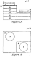
- Figures 1A and 1B illustrate a typical lateral GaN-based LED 20 that is fabricated on a sapphire substrate 22.
- an n-GaN buffer layer 24 is formed on the substrate 22.
- a relatively thick n-GaN layer 26 is formed on the buffer layer 24.
- An active layer 28 having multiple quantum wells of aluminum-indium-gallium-nitride (AlInGaN) or of InGaN/GaN is then formed on the n-type GaN layer 26.
- a p-GaN layer 30 is then formed on the active layer 26.
- a transparent conductive layer 32 is then formed on the p-GaN layer 30.
- the transparent conductive layer 32 may be made of any suitable material, such as Ru/Au, Ni/Au or indium-tin-oxide (ITO).
- a p-type electrode 34 is then formed on one side of the transparent conductive layer 32. Suitable p-type electrode materials include Ni/Au, Pd/Au, Pd/Ni and Pt.
- a pad 36 is then formed on the p-type electrode 34. Beneficially, the pad 36 is Au.
- the transparent conductive layer 32, the p-GaN layer 30, the active layer 28 and part of the n-GaN layer 26 are etched to form a step. Because of the difficulty of wet etching GaN, a dry etch is usually used to form the step. This etching requires additional lithography and stripping processes. Furthermore, plasma damage to the GaN step surface is often sustained during the dry-etch process.
- the LED 20 is completed by forming an n-electrode pad 38 (usually Au) and pad 40 on the step.
- Figure 1B illustrates a top down view of the LED 20.
- lateral GaN-based LEDs have a significant draw back in that having both metal contacts (36 and 40) on the same side of the LED significantly reduces the surface area available for light emission.
- the metal contacts 36 and 40 are physically close together.
- the pads 36 are often Au.
- Au spreading can bring the electrical contacts even closer together.
- Such closely spaced electrodes 34 are highly susceptible to ESD problems.
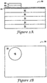
- Figures 2A and 2B illustrate a vertical GaN-based LED 50 that was formed on a sapphire substrate that was later removed.
- the LED 50 includes a GaN buffer layer 54 having an n-metal contact 56 on a bottom side and a relatively thick n-GaN layer 58 on the other.
- the n-metal contact 56 is beneficially formed from a high reflectively layer that is overlaid by a high conductivity metal (beneficially Au).
- An active layer 60 having multiple quantum wells is formed on the n-type GaN layer 58, and a p-GaN layer 62 is formed on the active layer 60.
- a transparent conductive layer 64 is then formed on the p-GaN layer 62, and a p-type electrode 66 is formed on the transparent conductive layer 64.
- a pad 68 is formed on the p-type electrode 66.
- the materials for the various layers are similar to those used in the lateral LED 20.
- the vertical GaN-based LED 50 as the advantage that etching a step is not required.
- the sapphire substrate (not shown) has to be removed. Such removal can be difficult, particularly if device yields are of concern.
- sapphire substrate removal using laser lift off is known. (see, United States Patent 6,071,795 to Cheung et al.
- vertical GaN-based LEDs have the advantage that only one metal contact (68) blocks light emission.
- lateral GaN-based LEDs must have larger surface areas, which causes lower device yields.
- the reflecting layer of the n-type contact 56 used in vertical GaN-based LEDs reflect light that is otherwise absorbed in lateral GaN-based LEDs.
- a lateral GaN-based LED must have a significantly larger surface area. Because of these issues, a 2" diameter sapphire wafer can produce about 35,000 vertical GaN-based LEDs, but only about 12,000 lateral GaN-based LEDs.
- the lateral topology is more vulnerable to static electricity, primarily because the two electrodes (36 and 40) are so close together. Additionally, as the lateral topology is fabricated on an insulating substrate, and as the vertical topology can be attached to a heat sink, the lateral topology has relatively poor thermal dissipation. Thus, in many respects the vertical topology is operationally superior to the lateral topology.
- GaN-based LEDs fabricated on insulating substrates have a lateral topology. This is primarily because of the difficulties of removing the insulating substrate and of handling the GaN wafer structure without a supporting substrate. Despite these problems, removal of an insulating (growth) substrate and subsequent wafer bonding of the resulting GaN-based wafer on a Si substrate using Pd/In metal layers has been demonstrated for very small area wafers, approx. 1 cm by 1 cm. (reported by the University of California at Berkley and the Xerox Corporation). But, substrate removal and subsequent wafer bonding of large area wafers remains very difficult due to inhomogeneous bonding between the GaN wafer and the 2 nd (substitutional) substrate. This is mainly due to wafer bowing during and after laser lift off.
- a method of removing semiconductor layers from a sapphire substrate, of isolating a wafer having the partially fabricated semiconductor devices such that wafer warping is reduced or prevented, followed by substitution of a metal supporting layer would be useful. More specifically, a method of partially fabricating GaN-based devices on a sapphire (or other insulating) substrate, followed by substitution of a conducting supporting layer, followed by dicing the substituting layer to yield vertical topology GaN-based LEDs would be beneficial.
- Document DE 200 09283 U1 discloses a GaN-based light-emitting device in which the substrate has been replaced by a metallic support.
- the principles of the present invention provide for a method of fabricating semiconductor devices on insulating substrates by first forming semiconductor layers on the insulating substrate, followed by removal of the insulating substrate to isolate a wafer having the formed semiconductor layers, followed by the addition of a metal support substrate (at the bottom of the semiconductor layers) that will support the wafer, all while supporting the wafer to prevent warping and/or other damage.
- the principles of the present invention further provide for a method of fabricating GaN-based vertical devices on insulating substrates using metal support films.
- semiconductor layers for the GaN-based devices are formed on an insulating (sapphire) substrate using normal semiconductor fabrication techniques.
- trenches are formed through the semiconductor layers and into the insulating substrate.
- the trenches are fabricated using inductive couple (inductively coupled) plasma reactive ion etching (ICPRIE).
- ICPRIE inductive couple plasma reactive ion etching
- a first support structure is attached to the semiconductor layers.
- the first support structure is comprised of silicon, but almost any hard flat surface is acceptable. That first support structure is beneficially attached to the semiconductive layers using an epoxy adhesive, possibly with a protective photo-resist layer over the semiconductive layer.
- the insulating substrate is removed, beneficially using a laser-lift off process.
- a second supporting structure is then substituted for the insulating substrate.
- the second supporting structure is comprised of a metal film of Cu, Au or Al, but almost any conductive film is acceptable.
- a conductive contact can be inserted between the semiconductive layer and the second supporting structure. In the case of LEDs, the conductive contact is beneficially reflective to bounce photons upward to prevent absorption in the bottom lead frame.
- the first supporting structure is then removed. Individual devices are then diced out, beneficially either by mechanical dicing or wet/dry etching through the second supporting structure.
- the following describes another way of forming metal support films on the semiconductor layers.
- This method does not form part of the present invention.
- Trench formation through the semiconductor layers and into the insulating substrate is identical to the procedure described above.
- a thick metal support film is deposited on top of the GaN-based devices using chemical and/or physical deposition techniques (such as electroplating or electro-less plating).
- the insulating substrate is removed, beneficially using a laser-lift off process.
- the thick metal support film is comprised of Cu, Au or Al, but almost any conductive film is acceptable. If required, a conductive contact can be inserted between the semiconductive layer and the second supporting structure.
- the conductive contact is beneficially reflective to bounce photons to prevent absorption in the bottom lead frame. Electrical contacts can then be formed on the exposed surface of the semiconductor layers. Individual devices can then diced out, beneficially either by mechanical dicing or wet/dry etching through the thick metal support film.
- the principles of the present invention specifically provide for a method of fabricating vertical topology GaN-based LEDs on sapphire substrates.
- semiconductor layers for the vertical topology GaN-based LEDs are formed on a sapphire substrate using normal semiconductor fabrication techniques.
- trenches are formed through the semiconductor layers and into the sapphire substrate. Those trenches define the boundaries of the individual vertical topology GaN-based LEDs.
- the trenches are fabricated using ICPRIE.
- a protective photo-resist layer is located over the semiconductor layers.
- a first support structure is then attached to the semiconductor layers.
- the first support structure is a silicon plate, but almost any hard flat material is acceptable.
- the first support structure is beneficially attached to the semiconductive layers (or photo-resist layer) using an epoxy adhesive. Then, the sapphire substrate is removed, beneficially using a laser lift off process. A conductive bottom contact is then located on the exposed semiconductor layer. That conductive bottom contact beneficially includes a reflective layer. One or more adhesion support layers, such as a Cr and/or and Au layer, is formed over the reflective layer. Then, a second supporting structure is substituted in place of the sapphire substrate. Beneficially, the second supporting structure is comprised of a conductive film of Cu, Au or Al, but almost any conductive film is acceptable. The first supporting structure is then removed. Finally, the individual device dies are diced out, beneficially either by mechanical dicing or by wet/dry etching through the second supporting structure. Mechanical rolling or shear cutting can be used to separate the dies.
- the sapphire substrate is removed, beneficially using a laser lift off process.
- Conductive bottom contacts are then located on the recently exposed semiconductor layer.
- the individual device dies are diced out, beneficially either by mechanical dicing or by wet/dry etching through the metal support structure.
- the principles of the present invention provide for methods of fabricating GaN-based vertical devices on insulating substrates using thick metal support films. While those principles are illustrated in a detailed description of a method of fabricating vertical topology GaN-based LEDs on a sapphire substrate, those principles are broader than that method. Therefore, the principles of the present invention are to be limited only by the appended claims.
- FIGs 3-25 illustrate methods of manufacturing vertical topology GaN-based light emitting diodes (LEDs) using sapphire substrates.
- Sapphire substrates are readily available in suitable sizes, are thermally, chemically, and mechanically stable, are relatively inexpensive, and support the growth of good quality GaN epitaxial layers.
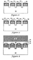
- a vertical topology GaN-based LED layer structure 120 that is similar or identical to the semiconductor layers of the vertical GaN-based LED 50 illustrated in Figures 2A and 2B is formed on a 330-430 micron-thick, 2" diameter sapphire substrate 122.
- the vertical topology GaN-based LED layer structure 120 can have an InGaN/GaN active layer (60) having the proper composition to emit blue light.
- the vertical topology GaN-based LED layer structure 120 is beneficially less than 5 microns thick.
- Various standard epitaxial growth techniques such as vapor phase epitaxy, MOCVD, and MBE, together with suitable dopants and other materials, can be used to produce the vertical topology GaN-based LED layer structure 120.
- trenches 124 are formed through the vertical topology GaN-based LED layer structure 120 and into the sapphire substrate 122.
- the trenches define the individual LED semiconductor structures that will be produced and separated.
- Each individual LED semiconductor structure is beneficially a square about 200 microns wide.
- the trenches are beneficially narrower than about 10 microns wide and extend deeper than about 5 microns into the sapphire substrate 122.
- the trenches 124 are beneficially formed in the structure of Figure 3 using reactive ion etching, preferably inductively coupled plasma reactive ion etching (ICP RIE).
- ICP RIE inductively coupled plasma reactive ion etching
- Forming trenches using ICP RIE has two main steps: forming scribe lines and etching. Scribe lines are formed on the structure of Figure 3 using a photo-resist pattern in which areas of the sapphire substrate 122 where the trenches 124 are to be formed are exposed. The exposed areas are the scribe lines and all other areas are covered by photo-resist.
- the photo-resist pattern is beneficially fabricated from a relatively hard photo-resist material that withstands intense plasma.
- the photo-resist could be AZ 9260, while the developer used to develop the photo-resist to form the scribe lines could be AZ MIF 500.
- the photo-resist is beneficially spin coated to a thickness of about 10 microns.
- the photo-resist thickness should be about the same as the thickness of the vertical topology GaN-based LED layer structure 120 plus the etch depth into the sapphire substrate 122. This helps ensure that the photo-resist mask remains intact during etching. Because it is difficult to form a thick photo-resist coating in one step, the photo-resist is beneficially applied in two coats, each about 5 microns thick. The first photo-resist coat is spin coated on and then soft baked at approximately 90 °F for about 15 minutes.
- the second photo-resist coat is applied in a similar manner, but is soft baked at approximately 110 °F for about 8 minutes.
- the photo-resist coating is then patterned to form the scribe lines. This is beneficially performed using lithographic techniques and development. Development takes a relatively long time because of the thickness of the photo-resist coating.
- the photo-resist pattern is hard baked at about 80 °F for about 30 minutes.
- the hard baked photo-resist is beneficially dipped in a MCB (Metal Chlorobenzene) treatment for about 3.5 minutes. Such dipping further hardens the photo-resist.
- MCB Metal Chlorobenzene
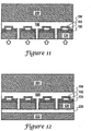
- the structure of Figure 3 is etched.
- the ICP RIE etch process is performed by placing the structure of Figure 3 on a bottom electrode 350 in a RIE chamber 352 having an insulating window 354 (beneficially a 1 cm-thick quartz window).
- the bottom electrode 350 is connected to a bias voltage supply 356 that biases the structure of Figure 3 to enable etching.
- the bias voltage supply 356 beneficially supplies 13.56 MHz RF power and a DC-bias voltage.
- the distance from the insulating window 354 to the bottom electrode 350 is beneficially about 6.5cm.
- a gas mixture of Cl 2 and BCl 3 , and possibly Ar, is injected into the RIE chamber 352 through a reactive gas port 360.
- a 2.5-turn or so spiral Cu coil 364 is located above the insulating window 354.
- Radio frequency (RF) power at 13.56 MHz is applied to the coil 364 from an RF source 366. It should be noted that magnetic fields are produced at right angles to the insulating window 354 by the RF power.
- the first procedure is to form a temporary substrate on top of the structure of Figure 4 .
- the other is to form a permanent metal layer on top of the structure of Figure 4 .
- the formation of a temporary substrate will be described first (with reference to Figures 6 through 15 ), followed by a description of the use of a permanent metal layer (with reference to Figures 16-20 ).
- thin transparent contacts 190 are formed on the individual LED semiconductor structures of the vertical topology GaN-based LED layer structure 120.
- Those transparent contacts 190 are beneficially comprised of Ru/Au, Ni/Au, or of indium tin oxide (ITO)/Au and are less than 10nm.
- metal contact pads 192 are placed on each transparent contact 190.
- the metal contact pads 192 are beneficially comprised of Pd, Pt, Au, or Al.
- Each metal contact pad 192 has a diameter of about 100 microns and a thickness of about 1 micron.
- a thin Cr/Au inter layer can be used to improve adhesion between transparent contacts 190 and the metal contact pad 192.
- a protective photo-resist film 196 is formed over the structure of Figure 7 . That photo-resist film is to protect the GaN-based LED layer structure 120 and to assist subsequent bonding.
- An epoxy adhesive 198 is then used to attach a first supporting structure that takes the form of a temporary supporting wafer 200.
- the temporary supporting wafer 200 is beneficially a silicon plate that is larger than the sapphire wafer. However, almost any hard, flat surface with a sufficient thickness to support a wafer containing the individual LED semiconductor devices during substrate swapping (described subsequently) is acceptable.
- the first substrate swapping processes is surface polishing and sand blasting (or surface roughening with a dry etching processes) the backside (the bottom side in Figure 8 ) of the sapphire substrate 122. This step helps to ensure uniform laser beam heating during a laser lift off step that is subsequently performed.
- a first vacuum chuck 210 attaches to the supporting wafer 200 and the second vacuum chuck 212 attaches to the sapphire substrate 122.
- a laser beam 214 is directed through the sapphire substrate 122.
- the laser beam 214 is beneficially from a 248 nm KrF laser having a 3 mm x 50 mm rectangular beam and beam energy between 200 ⁇ 600 mJ/cm 2 .
- the vacuum chucks 210 and 212 which are made of materials transparent to the 248 nm KrF laser beam, beneficially sapphire, bias the sapphire substrate 122 away from the supporting wafer 200.
- the combination of laser irradiation and bias causes the sapphire substrate 122 to separate as shown in Figure 10 .
- the bottom of the resulting structure (the side opposite the temporary supporting wafer 200) is first cleaned with HCl to remove Ga droplets (the laser beam 214 causes heating which separates the GaN into Ga+N).
- ICP RIE etching (see above) and polishing are performed. This etching and polishing exposes and produces an atomically flat surface of pure n-GaN. The flat surface is particularly beneficial in producing high reflectivity from a reflective structure that is deposited subsequently.
- the etched n-GaN surface is further cleaned and etched with aqua regia solution (mixture of H 2 SO 4 and HCl) to enhance the adhesion between n-GaN and Ti/Al metal layers.
- a conductive reflective structure comprised of a titanium layer 230 and an aluminum layer 232 is then formed on the bottom of the structure of Figure 11 . That reflective structure will reflect light from completed LEDs that is directed toward the bottom of the LEDs back out of the top of the LEDs.
- These bottom metal layers also serve as an n-type contact layer for the LED device.
- a second supporting structure in the form of a Cu, Au or Al thick film support 240 is formed on the Au adhesion layer 238.
- the thick film support 240 can be formed by physical vapor deposition by electroplating, by electro-less plating, or by other suitable means.
- This thick film support 240 is beneficially less than about 100 microns thick. While a Cu, Au or Al thick film support is beneficial, almost any electrically conductive, and beneficially thermally conductive, material is acceptable.
- the epoxy adhesive 198 and the temporary supporting wafer 200 are removed, reference Figure 15 .
- Such removal is beneficially achieved by heating the structure of Figure 14 to weaken the epoxy adhesive such that the temporary supporting wafer 200 can be removed.
- the resulting structure is immersed in acetone to remove any photo-resist and residual epoxy adhesive 198.
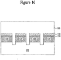
- a transparent metal layer 290 is formed on the vertical topology GaN-based LED layer structures 120.
- an adhesion layer 338 comprised of Cr and Au layers is located on the transparent metal layer 290.
- the thick metal support film 300 beneficially comprised of Cu, Au or Al, is formed on the adhesion layer 338.
- the thick metal support film 300 can be formed by physical vapor deposition, electro/ electro-less plating, or by other suitable means. This thick metal support film 300 is beneficially less than about 100 microns thick. While a Cu, Au or Al thick metal support film 300 is beneficial, almost any electrically conductive, and beneficially thermally conductive, material is acceptable.
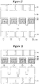
- FIG. 17 the structure shown in Figure 16 is then attached to two vacuum chucks.
- a first vacuum chuck 210 attaches to the thick metal support film 300 and the second vacuum chuck 212 attaches to the sapphire substrate 122.
- a laser beam 214 is directed through the sapphire substrate 122.
- the laser beam 214 is beneficially from a 248 nm KrF laser with 3 mm x 50 mm rectangular beam and beam energy in between 200 ⁇ 600 mJ/cm2.
- the vacuum chucks 210 and 212 which are made of materials transparent to the 248 nm KrF laser beam, beneficially sapphire, bias the sapphire substrate 122 away from the GaN-LED devices backed with thick metal support film 300.
- the combination of laser irradiation and bias causes the sapphire substrate 122 to separate as shown in Figure 18 .
- the bottom of the resulting structure (the side opposite the thick metal film 240) is first cleaned with HCl to remove Ga droplets (the laser beam 214 causes heating which separates the GaN into Ga+N).
- ICP RIE etching (see above) and polishing are performed. This etching and polishing exposes and produces an atomically flat surface of pure n-GaN.
- the etched n-GaN surface is further cleaned and etched with aqua regia solution (mixture of H 2 SO 4 and HCl) to enhance the adhesion between n-GaN and Ti/Al metal layers.
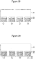
- electrical contacts are formed on the individual vertical topology GaN-based LED layer structures 120.
- Those electrical contacts beneficially include a Ti/Al interface layer 330 to the vertical topology GaN-based LED layer structures 120, and a Cr/Au contact pad 332 on the Ti/Al interface layer 330.
- dicing is beneficially accomplished by depositing a photo-resist pattern 250 on the thick film support 240. That photo-resist pattern 250 is then developed to expose areas of the thick film support 240 that align with the trenches 124. Openings 254 are then etched through the thick film support 240. The photo-resist pattern 250 is then removed.
- a mounting tape 260 can be placed on top of the structure of Figure 21 . Then, a roller can roll over the mounting tape to stress the remaining intact layers such that the individual devices are diced out.
- the mounting tape 260 can be located on the bottom of the structure of Figure 21 . Then, a diamond-cutting wheel 262 can dice out the individual devices.
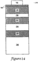
- each LED includes a thick film support 240, an adhesion support (Cr adhesion layer 236 and Au adhesion layer 238), a reflective structure (titanium layer 230 and aluminum layer 232), semiconductor layers 120 and top contacts (transparent contact 190 and metal contact pad 192).
- Those semiconductor layers include semiconductor layers as shown in Figure 2A .
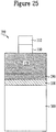
- a thick metal support film 300 is used, the result is the LED 399 shown in Figure 25 .
- That LED includes a thick metal support film 300, an adhesion layer 338, a reflective and p-type transparent contact 290, semiconductor layers 120, an n-type top interface layer 330, and a contact pad 332.
- Those semiconductor layers include semiconductor layers as shown in Figure 2A .
Landscapes
- Engineering & Computer Science (AREA)
- Microelectronics & Electronic Packaging (AREA)
- Manufacturing & Machinery (AREA)
- Computer Hardware Design (AREA)
- Power Engineering (AREA)
- Led Devices (AREA)
- Weting (AREA)
Description
- The present invention relates to semiconductor device fabrication. More particularly, the present invention relates to a method of fabricating vertical devices using a metal support film.
- Light emitting diodes ("LEDs") are well-known semiconductor devices that convert current into light. The color of the light (wavelength) that is emitted by an LED depends on the semiconductor material that is used to fabricate the LED. This is because the wavelength of the emitted light depends on the semiconductor material's band-gap energy, which represents the energy difference between valence band and conduction band electrons.
- Gallium-Nitride (GaN) has gained much attention from LED researchers. One reason for this is that GaN can be combined with indium to produce InGaN/GaN semiconductor layers that emit green, blue, and white visible light. This wavelength control ability enables an LED semiconductor designer to tailor material characteristics to achieve beneficial device characteristics. For example, GaN enables an LED semiconductor designer to produce blue LEDs and blue laser diodes, which are beneficial in full color displays and in optical recordings, and white LEDs, which can replace incandescent lamps.
- Because of the foregoing and other advantageous, the market for GaN-based LEDs is rapidly growing. Accordingly, GaN-based opto-electronic device technology has rapidly evolved since their commercial introduction in 1994. Because the efficiency of GaN light emitting diodes has surpassed that of incandescent lighting, and is now comparable with that of fluorescent lighting, the market for GaN based LEDs is expected to continue its rapid growth.
- Despite the rapid development of GaN device technology, GaN devices are too expensive for many applications. One reason for this is the high cost of manufacturing GaN-based devices, which in turn is related to the difficulties of growing GaN epitaxial layers and of subsequently dicing out completed GaN-based devices.
- GaN-based devices are typically fabricated on sapphire substrates. This is because sapphire wafers are commercially available in dimensions that are suitable for mass-producing GaN-based devices, because sapphire supports high-quality GaN epitaxial layer growths, and because of the extensive temperature handling capability of sapphire. Typically, GaN-based devices are fabricated on 2" diameter sapphire wafers that are either 330 or 430 microns thick. Such a diameter enables the fabrication of thousands of individual devices, while the thickness is sufficient to support device fabrication without excessive wafer warping. Furthermore, the sapphire crystal is chemically and thermally stable, has a high melting temperature that enables high temperature fabrication processes, has a high bonding energy (122.4 Kcal/mole), and a high dielectric constant. Chemically, sapphires are crystalline aluminum oxide, Al2O3.
- Fabricating semiconductor devices on sapphire is typically performed by growing an n-GaN epitaxial layer on a sapphire substrate using metal oxide chemical vapor deposition (MOCVD) or molecular beam epitaxy (MBE). Then, a plurality of individual devices, such as GaN LEDs, is fabricated on the epitaxial layer using normal semiconductor processing techniques. After the individual devices are fabricated they must be diced out of the sapphire substrate. However, since sapphires are extremely hard, are chemically resistant, and do not have natural cleave angles, sapphire substrates are difficult to dice. Indeed, dicing typically requires that the sapphire substrate be thinned to about 100 microns by mechanical grinding, lapping, and/or polishing. It should be noted that such mechanical steps are time consuming and expensive, and that such steps reduce device yields. Even after thinning sapphires remain difficult to dice. Thus, after thinning and polishing, the sapphire substrate is usually attached to a supporting tape. Then, a diamond saw or stylus forms scribe lines between the individual devices. Such scribing typically requires at least half an hour to process one substrate, adding even more to the manufacturing costs. Additionally, since the scribe lines have to be relatively wide to enable subsequent dicing, the device yields are reduced, adding even more to manufacturing costs. After scribing, the sapphire substrates are rolled using a rubber roller to produce stress cracks that propagate from the scribe lines and that subsequently dice out the individual semiconductor devices. This mechanical handling reduces yields even more.
- In addition to the foregoing problem of dicing individual devices from sapphire substrates, or in general other insulating substrate, sapphire substrates or other insulating substrate have other drawbacks. Of note, because sapphire is an insulator, the device topologies that are available when using sapphire substrates (or other insulating substrates) are limited. In practice there are only two device topologies: lateral and vertical. In the lateral topology the metallic electrical contacts that are used to inject current are both located on upper surfaces. In the vertical topology the substrate is removed, one metallic contact is on the upper surface and the other contact is on the lower surface.
-
Figures 1A and 1B illustrate a typical lateral GaN-basedLED 20 that is fabricated on asapphire substrate 22. Referring now specifically toFigure 1A , an n-GaN buffer layer 24 is formed on thesubstrate 22. A relatively thick n-GaN layer 26 is formed on thebuffer layer 24. Anactive layer 28 having multiple quantum wells of aluminum-indium-gallium-nitride (AlInGaN) or of InGaN/GaN is then formed on the n-type GaN layer 26. A p-GaN layer 30 is then formed on theactive layer 26. A transparentconductive layer 32 is then formed on the p-GaN layer 30. The transparentconductive layer 32 may be made of any suitable material, such as Ru/Au, Ni/Au or indium-tin-oxide (ITO). A p-type electrode 34 is then formed on one side of the transparentconductive layer 32. Suitable p-type electrode materials include Ni/Au, Pd/Au, Pd/Ni and Pt. Apad 36 is then formed on the p-type electrode 34. Beneficially, thepad 36 is Au. The transparentconductive layer 32, the p-GaN layer 30, theactive layer 28 and part of the n-GaN layer 26 are etched to form a step. Because of the difficulty of wet etching GaN, a dry etch is usually used to form the step. This etching requires additional lithography and stripping processes. Furthermore, plasma damage to the GaN step surface is often sustained during the dry-etch process. TheLED 20 is completed by forming an n-electrode pad 38 (usually Au) andpad 40 on the step. -
Figure 1B illustrates a top down view of theLED 20. As can be seen, lateral GaN-based LEDs have a significant draw back in that having both metal contacts (36 and 40) on the same side of the LED significantly reduces the surface area available for light emission. As shown inFigure 1B themetal contacts pads 36 are often Au. When external wire bonds are attached to thepads -
Figures 2A and 2B illustrate a vertical GaN-basedLED 50 that was formed on a sapphire substrate that was later removed. Referring now specifically toFigure 2A , theLED 50 includes aGaN buffer layer 54 having an n-metal contact 56 on a bottom side and a relatively thick n-GaN layer 58 on the other. The n-metal contact 56 is beneficially formed from a high reflectively layer that is overlaid by a high conductivity metal (beneficially Au). Anactive layer 60 having multiple quantum wells is formed on the n-type GaN layer 58, and a p-GaN layer 62 is formed on theactive layer 60. A transparentconductive layer 64 is then formed on the p-GaN layer 62, and a p-type electrode 66 is formed on the transparentconductive layer 64. Apad 68 is formed on the p-type electrode 66. The materials for the various layers are similar to those used in thelateral LED 20. The vertical GaN-basedLED 50 as the advantage that etching a step is not required. However, to locate the n-metal contact 56 below theGaN buffer layer 54 the sapphire substrate (not shown) has to be removed. Such removal can be difficult, particularly if device yields are of concern. However, as discussed subsequently, sapphire substrate removal using laser lift off is known. (see, United States Patent6,071,795 to Cheung et al. , entitled, "Separation of Thin Films From Transparent Substrates By Selective Optical Processing," issued on June 6, 2000, and Kelly et al. "Optical process for liftoff of group III-nitride films", Physica Status Solidi (a) vol. 159, 1997, pp. R3-R4). - Referring now to
Figure 2B , vertical GaN-based LEDs have the advantage that only one metal contact (68) blocks light emission. Thus, to provide the same amount of light emission area lateral GaN-based LEDs must have larger surface areas, which causes lower device yields. Furthermore, the reflecting layer of the n-type contact 56 used in vertical GaN-based LEDs reflect light that is otherwise absorbed in lateral GaN-based LEDs. Thus, to emit the same amount of light as a vertical GaN-based LED, a lateral GaN-based LED must have a significantly larger surface area. Because of these issues, a 2" diameter sapphire wafer can produce about 35,000 vertical GaN-based LEDs, but only about 12,000 lateral GaN-based LEDs. Furthermore, the lateral topology is more vulnerable to static electricity, primarily because the two electrodes (36 and 40) are so close together. Additionally, as the lateral topology is fabricated on an insulating substrate, and as the vertical topology can be attached to a heat sink, the lateral topology has relatively poor thermal dissipation. Thus, in many respects the vertical topology is operationally superior to the lateral topology. - However, most GaN-based LEDs fabricated on insulating substrates have a lateral topology. This is primarily because of the difficulties of removing the insulating substrate and of handling the GaN wafer structure without a supporting substrate. Despite these problems, removal of an insulating (growth) substrate and subsequent wafer bonding of the resulting GaN-based wafer on a Si substrate using Pd/In metal layers has been demonstrated for very small area wafers, approx. 1 cm by 1 cm. (reported by the University of California at Berkley and the Xerox Corporation). But, substrate removal and subsequent wafer bonding of large area wafers remains very difficult due to inhomogeneous bonding between the GaN wafer and the 2nd (substitutional) substrate. This is mainly due to wafer bowing during and after laser lift off.
- Thus, it is apparent that a better method of substituting a 2nd (substitutional) substrate for the original (growth) insulating substrate would be beneficial. In particular, a method that provides for mechanical stability of the wafer, that supports good electrical contact, and that assists heat dissipation would be highly useful, particularly for devices subject to high electrical current injection, such as laser diodes or high power LEDs. This would enable forming semiconductor layers on an insulating substrate, followed by removal of the insulating substrate to isolate a wafer having the formed semiconductor layers, followed by subsequent attachment of the wafer to a metal substitutional substrate. Of particular benefit would be a new method suitable for removing sapphire substrates from partially fabricated semiconductor devices, particularly if those devices are GaN-based. For example, a method of removing semiconductor layers from a sapphire substrate, of isolating a wafer having the partially fabricated semiconductor devices such that wafer warping is reduced or prevented, followed by substitution of a metal supporting layer would be useful. More specifically, a method of partially fabricating GaN-based devices on a sapphire (or other insulating) substrate, followed by substitution of a conducting supporting layer, followed by dicing the substituting layer to yield vertical topology GaN-based LEDs would be beneficial.
-
Document DE 200 09283 U1 discloses a GaN-based light-emitting device in which the substrate has been replaced by a metallic support. - The following summary of the invention is provided to facilitate an understanding of some of the innovative features unique to the present invention, and is not intended to be a full description. A full appreciation of the various aspects of the invention can be gained by taking the entire specification, claims, drawings, and abstract as a whole
- The principles of the present invention provide for a method of fabricating semiconductor devices on insulating substrates by first forming semiconductor layers on the insulating substrate, followed by removal of the insulating substrate to isolate a wafer having the formed semiconductor layers, followed by the addition of a metal support substrate (at the bottom of the semiconductor layers) that will support the wafer, all while supporting the wafer to prevent warping and/or other damage.
- The principles of the present invention further provide for a method of fabricating GaN-based vertical devices on insulating substrates using metal support films. According to that method, semiconductor layers for the GaN-based devices are formed on an insulating (sapphire) substrate using normal semiconductor fabrication techniques. Then, trenches are formed through the semiconductor layers and into the insulating substrate. Beneficially, the trenches are fabricated using inductive couple (inductively coupled) plasma reactive ion etching (ICPRIE). Then, a first support structure is attached to the semiconductor layers. Beneficially, the first support structure is comprised of silicon, but almost any hard flat surface is acceptable. That first support structure is beneficially attached to the semiconductive layers using an epoxy adhesive, possibly with a protective photo-resist layer over the semiconductive layer. Then, the insulating substrate is removed, beneficially using a laser-lift off process. A second supporting structure is then substituted for the insulating substrate. Beneficially, the second supporting structure is comprised of a metal film of Cu, Au or Al, but almost any conductive film is acceptable. If required, a conductive contact can be inserted between the semiconductive layer and the second supporting structure. In the case of LEDs, the conductive contact is beneficially reflective to bounce photons upward to prevent absorption in the bottom lead frame. The first supporting structure is then removed. Individual devices are then diced out, beneficially either by mechanical dicing or wet/dry etching through the second supporting structure.
- The following describes another way of forming metal support films on the semiconductor layers. This method does not form part of the present invention. Trench formation through the semiconductor layers and into the insulating substrate is identical to the procedure described above. Then, instead of attaching the semiconductor layers onto the support structure (Si or a hard flat surface), a thick metal support film is deposited on top of the GaN-based devices using chemical and/or physical deposition techniques (such as electroplating or electro-less plating). Then, the insulating substrate is removed, beneficially using a laser-lift off process. Beneficially, the thick metal support film is comprised of Cu, Au or Al, but almost any conductive film is acceptable. If required, a conductive contact can be inserted between the semiconductive layer and the second supporting structure. In the case of LEDs, the conductive contact is beneficially reflective to bounce photons to prevent absorption in the bottom lead frame. Electrical contacts can then be formed on the exposed surface of the semiconductor layers. Individual devices can then diced out, beneficially either by mechanical dicing or wet/dry etching through the thick metal support film.
- The principles of the present invention specifically provide for a method of fabricating vertical topology GaN-based LEDs on sapphire substrates. According to that method, semiconductor layers for the vertical topology GaN-based LEDs are formed on a sapphire substrate using normal semiconductor fabrication techniques. Then, trenches are formed through the semiconductor layers and into the sapphire substrate. Those trenches define the boundaries of the individual vertical topology GaN-based LEDs. Beneficially, the trenches are fabricated using ICPRIE. Then, a protective photo-resist layer is located over the semiconductor layers. A first support structure is then attached to the semiconductor layers. Beneficially, the first support structure is a silicon plate, but almost any hard flat material is acceptable. The first support structure is beneficially attached to the semiconductive layers (or photo-resist layer) using an epoxy adhesive. Then, the sapphire substrate is removed, beneficially using a laser lift off process. A conductive bottom contact is then located on the exposed semiconductor layer. That conductive bottom contact beneficially includes a reflective layer. One or more adhesion support layers, such as a Cr and/or and Au layer, is formed over the reflective layer. Then, a second supporting structure is substituted in place of the sapphire substrate. Beneficially, the second supporting structure is comprised of a conductive film of Cu, Au or Al, but almost any conductive film is acceptable. The first supporting structure is then removed. Finally, the individual device dies are diced out, beneficially either by mechanical dicing or by wet/dry etching through the second supporting structure. Mechanical rolling or shear cutting can be used to separate the dies.
- There is also provided another method of fabricating vertical topology GaN-based LEDs on sapphire substrates. According to that method, which does not form part of the invention, semiconductor layers for the vertical topology GaN-based LEDs are formed on a sapphire substrate using normal semiconductor fabrication techniques. Then, trenches are formed through the semiconductor layers and into the sapphire substrate. Those trenches define the boundaries of the individual vertical topology GaN-based LEDs. Beneficially, the trenches are fabricated using ICPRIE. Then, a contact layer comprised, for example, of layers of Cr and Au is located over the semiconductor layers. Then a metal support structure is then formed over the contact layer/semiconductor layers. Then, the sapphire substrate is removed, beneficially using a laser lift off process. Conductive bottom contacts are then located on the recently exposed semiconductor layer. Finally, the individual device dies are diced out, beneficially either by mechanical dicing or by wet/dry etching through the metal support structure.
- The novel features of the present invention will become apparent to those of skill in the art upon examination of the following detailed description of the invention or can be learned by practice of the present invention. It should be understood, however, that the detailed description of the invention and the specific examples presented, while indicating certain embodiments of the present invention, are provided for illustration purposes only.
- The accompanying figures, in which like reference numerals refer to identical or functionally-similar elements throughout the separate views and which are incorporated in and form part of the specification, further illustrate the present invention and, together with the detailed description of the invention, serve to explain the principles of the present invention.
- In the drawings:
-
Figure 1A illustrates a sectional view of a typical lateral topology GaN-based LED; -
Figure 1B shows a top down view of the GaN-based LED illustrated inFigure 1A ; -
Figure 2A illustrates a sectional view of a typical vertical topology GaN-based LED; -
Figure 2B shows a top down view of the GaN-based LED illustrated inFigure 2A ; and -
Figures 3-15 and21-24 illustrate steps of forming light emitting diodes that are in accord with the principles of the present invention. -
Figures 16-20 and25 illustrate steps of forming light emitting diodes that do not form part of the present invention. - The principles of the present invention provide for methods of fabricating GaN-based vertical devices on insulating substrates using thick metal support films. While those principles are illustrated in a detailed description of a method of fabricating vertical topology GaN-based LEDs on a sapphire substrate, those principles are broader than that method. Therefore, the principles of the present invention are to be limited only by the appended claims.
-
Figures 3-25 illustrate methods of manufacturing vertical topology GaN-based light emitting diodes (LEDs) using sapphire substrates. Sapphire substrates are readily available in suitable sizes, are thermally, chemically, and mechanically stable, are relatively inexpensive, and support the growth of good quality GaN epitaxial layers. - Referring now to
Figure 3 , a vertical topology GaN-basedLED layer structure 120 that is similar or identical to the semiconductor layers of the vertical GaN-basedLED 50 illustrated inFigures 2A and 2B is formed on a 330-430 micron-thick, 2"diameter sapphire substrate 122. For example, the vertical topology GaN-basedLED layer structure 120 can have an InGaN/GaN active layer (60) having the proper composition to emit blue light. The vertical topology GaN-basedLED layer structure 120 is beneficially less than 5 microns thick. Various standard epitaxial growth techniques, such as vapor phase epitaxy, MOCVD, and MBE, together with suitable dopants and other materials, can be used to produce the vertical topology GaN-basedLED layer structure 120. - Referring now to
Figure 4 ,trenches 124 are formed through the vertical topology GaN-basedLED layer structure 120 and into thesapphire substrate 122. The trenches define the individual LED semiconductor structures that will be produced and separated. Each individual LED semiconductor structure is beneficially a square about 200 microns wide. The trenches are beneficially narrower than about 10 microns wide and extend deeper than about 5 microns into thesapphire substrate 122. - Because of the hardness of sapphire and GaN, the
trenches 124 are beneficially formed in the structure ofFigure 3 using reactive ion etching, preferably inductively coupled plasma reactive ion etching (ICP RIE). Forming trenches using ICP RIE has two main steps: forming scribe lines and etching. Scribe lines are formed on the structure ofFigure 3 using a photo-resist pattern in which areas of thesapphire substrate 122 where thetrenches 124 are to be formed are exposed. The exposed areas are the scribe lines and all other areas are covered by photo-resist. The photo-resist pattern is beneficially fabricated from a relatively hard photo-resist material that withstands intense plasma. For example, the photo-resist could be AZ 9260, while the developer used to develop the photo-resist to form the scribe lines could be AZ MIF 500. - In the illustrated example, the photo-resist is beneficially spin coated to a thickness of about 10 microns. However, in general, the photo-resist thickness should be about the same as the thickness of the vertical topology GaN-based
LED layer structure 120 plus the etch depth into thesapphire substrate 122. This helps ensure that the photo-resist mask remains intact during etching. Because it is difficult to form a thick photo-resist coating in one step, the photo-resist is beneficially applied in two coats, each about 5 microns thick. The first photo-resist coat is spin coated on and then soft baked at approximately 90 °F for about 15 minutes. Then, the second photo-resist coat is applied in a similar manner, but is soft baked at approximately 110 °F for about 8 minutes. The photo-resist coating is then patterned to form the scribe lines. This is beneficially performed using lithographic techniques and development. Development takes a relatively long time because of the thickness of the photo-resist coating. After development, the photo-resist pattern is hard baked at about 80 °F for about 30 minutes. Then, the hard baked photo-resist is beneficially dipped in a MCB (Metal Chlorobenzene) treatment for about 3.5 minutes. Such dipping further hardens the photo-resist. - After the scribe lines are defined, the structure of
Figure 3 is etched. Referring now toFigure 5 , the ICP RIE etch process is performed by placing the structure ofFigure 3 on abottom electrode 350 in aRIE chamber 352 having an insulating window 354 (beneficially a 1 cm-thick quartz window). Thebottom electrode 350 is connected to abias voltage supply 356 that biases the structure ofFigure 3 to enable etching. Thebias voltage supply 356 beneficially supplies 13.56 MHz RF power and a DC-bias voltage. The distance from the insulatingwindow 354 to thebottom electrode 350 is beneficially about 6.5cm. A gas mixture of Cl2 and BCl3, and possibly Ar, is injected into theRIE chamber 352 through areactive gas port 360. Furthermore, electrons are injected into the chamber via aport 362. A 2.5-turn or sospiral Cu coil 364 is located above the insulatingwindow 354. Radio frequency (RF) power at 13.56 MHz is applied to thecoil 364 from anRF source 366. It should be noted that magnetic fields are produced at right angles to the insulatingwindow 354 by the RF power. - Still referring to
Figure 5 , electrons present in the electromagnetic field produced by thecoil 364 collide with neutral particles of the injected gases, resulting in the formation of ions and neutrals, which produce plasma. Ions in the plasma are accelerated toward the structure ofFigure 3 by the bias voltage applied by thebias voltage supply 356 to thebottom electrode 350. The accelerated ions pass through the scribe lines, forming the etch channels 124 (seeFigure 4 ). - With the structure of
Figure 4 , fabrication proceeds using one of two general procedures. The first procedure is to form a temporary substrate on top of the structure ofFigure 4 . The other is to form a permanent metal layer on top of the structure ofFigure 4 . The formation of a temporary substrate will be described first (with reference toFigures 6 through 15 ), followed by a description of the use of a permanent metal layer (with reference toFigures 16-20 ). - Referring now to
Figure 6 , after thetrenches 124 are formed, thintransparent contacts 190 are formed on the individual LED semiconductor structures of the vertical topology GaN-basedLED layer structure 120. Thosetransparent contacts 190 are beneficially comprised of Ru/Au, Ni/Au, or of indium tin oxide (ITO)/Au and are less than 10nm. As shown inFigure 7 , after thetransparent contacts 190 are formed,metal contact pads 192 are placed on eachtransparent contact 190. Themetal contact pads 192 are beneficially comprised of Pd, Pt, Au, or Al. Eachmetal contact pad 192 has a diameter of about 100 microns and a thickness of about 1 micron. A thin Cr/Au inter layer can be used to improve adhesion betweentransparent contacts 190 and themetal contact pad 192. - Referring now to
Figure 8 , a protective photo-resistfilm 196 is formed over the structure ofFigure 7 . That photo-resist film is to protect the GaN-basedLED layer structure 120 and to assist subsequent bonding. Anepoxy adhesive 198 is then used to attach a first supporting structure that takes the form of a temporary supportingwafer 200. The temporary supportingwafer 200 is beneficially a silicon plate that is larger than the sapphire wafer. However, almost any hard, flat surface with a sufficient thickness to support a wafer containing the individual LED semiconductor devices during substrate swapping (described subsequently) is acceptable. Still referring toFigure 8 , the first substrate swapping processes is surface polishing and sand blasting (or surface roughening with a dry etching processes) the backside (the bottom side inFigure 8 ) of thesapphire substrate 122. This step helps to ensure uniform laser beam heating during a laser lift off step that is subsequently performed. - Turning now to
Figure 9 , the structure shown inFigure 8 is then attached to two vacuum chucks. Afirst vacuum chuck 210 attaches to the supportingwafer 200 and thesecond vacuum chuck 212 attaches to thesapphire substrate 122. Then, still with reference toFigure 9 , alaser beam 214 is directed through thesapphire substrate 122. Thelaser beam 214 is beneficially from a 248 nm KrF laser having a 3 mm x 50 mm rectangular beam and beam energy between 200 ∼ 600 mJ/cm2. The vacuum chucks 210 and 212, which are made of materials transparent to the 248 nm KrF laser beam, beneficially sapphire, bias thesapphire substrate 122 away from the supportingwafer 200. The combination of laser irradiation and bias causes thesapphire substrate 122 to separate as shown inFigure 10 . - Similar laser lift off processes are described in United States Patent
6,071,795 to Cheung et al. , entitled, "Separation of Thin Films From Transparent Substrates By Selective Optical Processing," issued on June 6, 2000, and in Kelly et al. "Optical process for liftoff of group III-nitride films," Physica Status Solidi (a) vol. 159, 1997, pp. R3-R4. Beneficially, the temporary supportingwafer 200 fully supports the individual LED semiconductor structures in the vertical topology GaN-basedLED layer structure 120 in a manner the resists warping. - Turning now to
Figure 11 , after thesapphire substrate 122 is removed, the bottom of the resulting structure (the side opposite the temporary supporting wafer 200) is first cleaned with HCl to remove Ga droplets (thelaser beam 214 causes heating which separates the GaN into Ga+N). After cleaning, ICP RIE etching (see above) and polishing are performed. This etching and polishing exposes and produces an atomically flat surface of pure n-GaN. The flat surface is particularly beneficial in producing high reflectivity from a reflective structure that is deposited subsequently. Prior to reflective layer deposition, the etched n-GaN surface is further cleaned and etched with aqua regia solution (mixture of H2SO4 and HCl) to enhance the adhesion between n-GaN and Ti/Al metal layers. - Turning now to
Figure 12 , a conductive reflective structure comprised of atitanium layer 230 and analuminum layer 232 is then formed on the bottom of the structure ofFigure 11 . That reflective structure will reflect light from completed LEDs that is directed toward the bottom of the LEDs back out of the top of the LEDs. These bottom metal layers also serve as an n-type contact layer for the LED device. - Turning now to
Figure 13 , to assist formation of a subsequently produced second supporting structure, aCr adhesion layer 236, which is less than about 30 nm thick, is formed on theAl layer 232 and anAu adhesion layer 238, which is less than about 100 nm thick, is formed on theCr adhesion layer 236. - Turning now to
Figure 14 , after theAu adhesion layer 238 is in place a second supporting structure in the form of a Cu, Au or Althick film support 240 is formed on theAu adhesion layer 238. Thethick film support 240 can be formed by physical vapor deposition by electroplating, by electro-less plating, or by other suitable means. Thisthick film support 240 is beneficially less than about 100 microns thick. While a Cu, Au or Al thick film support is beneficial, almost any electrically conductive, and beneficially thermally conductive, material is acceptable. - After the
thick support 240 is in place, theepoxy adhesive 198 and the temporary supportingwafer 200 are removed, referenceFigure 15 . Such removal is beneficially achieved by heating the structure ofFigure 14 to weaken the epoxy adhesive such that the temporary supportingwafer 200 can be removed. After the temporary supportingwafer 200 is removed the resulting structure is immersed in acetone to remove any photo-resist and residualepoxy adhesive 198. - The process steps illustrated in
Figures 6 through 15 provide for a general fabrication process that uses atemporary support structure 200. Referring now toFigure 16 , an alternative method, which does not form part of the present invention, uses a thickmetal support film 300 that is formed on top of the structure ofFigure 4 . - First, a
transparent metal layer 290 is formed on the vertical topology GaN-basedLED layer structures 120. Then, anadhesion layer 338 comprised of Cr and Au layers is located on thetransparent metal layer 290. Then, the thickmetal support film 300, beneficially comprised of Cu, Au or Al, is formed on theadhesion layer 338. The thickmetal support film 300 can be formed by physical vapor deposition, electro/ electro-less plating, or by other suitable means. This thickmetal support film 300 is beneficially less than about 100 microns thick. While a Cu, Au or Al thickmetal support film 300 is beneficial, almost any electrically conductive, and beneficially thermally conductive, material is acceptable. - Turning now to
Figure 17 , the structure shown inFigure 16 is then attached to two vacuum chucks. Afirst vacuum chuck 210 attaches to the thickmetal support film 300 and thesecond vacuum chuck 212 attaches to thesapphire substrate 122. Then, still with reference toFigure 17 , alaser beam 214 is directed through thesapphire substrate 122. Thelaser beam 214 is beneficially from a 248 nm KrF laser with 3 mm x 50 mm rectangular beam and beam energy in between 200 ∼ 600 mJ/cm2. The vacuum chucks 210 and 212, which are made of materials transparent to the 248 nm KrF laser beam, beneficially sapphire, bias thesapphire substrate 122 away from the GaN-LED devices backed with thickmetal support film 300. The combination of laser irradiation and bias causes thesapphire substrate 122 to separate as shown inFigure 18 . - Similar laser lift off processes are described in United States Patent
6,071,795 to Cheung et al. , entitled, "Separation of Thin Films From Transparent Substrates By Selective Optical Processing," issued on June 6, 2000, and in Kelly et al. "Optical process for liftoff of group III-nitride films," Physica Status Solidi (a) vol. 159, 1997, pp. R3-R4. Beneficially, the supportingwafer 200 fully supports the individual LED semiconductor structures in the vertical topology GaN-basedLED layer structure 120. - Turning now to
Figure 19 , after thesapphire substrate 122 is removed, the bottom of the resulting structure (the side opposite the thick metal film 240) is first cleaned with HCl to remove Ga droplets (thelaser beam 214 causes heating which separates the GaN into Ga+N). After cleaning, ICP RIE etching (see above) and polishing are performed. This etching and polishing exposes and produces an atomically flat surface of pure n-GaN. Prior to n-type contact formation, the etched n-GaN surface is further cleaned and etched with aqua regia solution (mixture of H2SO4 and HCl) to enhance the adhesion between n-GaN and Ti/Al metal layers. - Referring now to
Figure 20 , after etching and polishing exposes and produces an atomically flat surface (seeFigure 19 ), electrical contacts are formed on the individual vertical topology GaN-basedLED layer structures 120. Those electrical contacts beneficially include a Ti/Al interface layer 330 to the vertical topology GaN-basedLED layer structures 120, and a Cr/Au contact pad 332 on the Ti/Al interface layer 330. - After removal of the temporary supporting
wafer 200 to leave the structure shown inFigure 15 , or after formation of the Cr/Au contact layer 332 to leave the structure shown inFigure 20 , the individual LED devices are ready to be diced out. Dicing can be accomplished in many ways, for example, by chemical/electrochemical etching or by mechanical action. As the basic dicing operations are the same, dicing will be described with specific reference to the structure shown inFigure 15 , with the understanding that dicing the structure ofFigure 20 is similar. Referring now toFigure 21 , dicing is beneficially accomplished by depositing a photo-resistpattern 250 on thethick film support 240. That photo-resistpattern 250 is then developed to expose areas of thethick film support 240 that align with thetrenches 124.Openings 254 are then etched through thethick film support 240. The photo-resistpattern 250 is then removed. - Actual separation of the individual devices can be accomplished in several ways. For example, as shown in
Figure 22 , a mountingtape 260 can be placed on top of the structure ofFigure 21 . Then, a roller can roll over the mounting tape to stress the remaining intact layers such that the individual devices are diced out. Alternatively, as shown inFigure 23 , the mountingtape 260 can be located on the bottom of the structure ofFigure 21 . Then, a diamond-cutting wheel 262 can dice out the individual devices. - The result is a plurality of vertical
topology GaN LEDs 199 on conductive substrates. As shown inFigure 24 , each LED includes athick film support 240, an adhesion support (Cr adhesion layer 236 and Au adhesion layer 238), a reflective structure (titanium layer 230 and aluminum layer 232), semiconductor layers 120 and top contacts (transparent contact 190 and metal contact pad 192). Those semiconductor layers include semiconductor layers as shown inFigure 2A . - Alternatively, in a process which is not part of the invention, a thick
metal support film 300 is used, the result is theLED 399 shown inFigure 25 . That LED includes a thickmetal support film 300, anadhesion layer 338, a reflective and p-typetransparent contact 290, semiconductor layers 120, an n-typetop interface layer 330, and acontact pad 332. Those semiconductor layers include semiconductor layers as shown inFigure 2A . - The embodiments and examples set forth herein are presented to best explain the present invention and its practical application and to thereby enable those skilled in the art to make and utilize the invention. Those skilled in the art, however, will recognize that the foregoing description and examples have been presented for the purpose of illustration and example only. It is intended that the scope of the present invention be defined by the claims appended hereto, giving full cognizance to equivalents in all respects.
Claims (16)
- A vertical topology light emitting device, comprising:a conductive adhesion structure (236, 238) comprising a first adhesion layer (238) having a first surface and a second adhesion layer (236) having a second surface;a conductive support structure (240) on the first surface;a reflective structure (230, 232) on the second surface, the reflective structure serving as a first electrical contact;a semiconductor structure (120) on the reflective structure, the semiconductor structure comprises a first-type GaN-based layer, an active layer on the first-type GaN-based layer, and a second-type GaN-based layer on the active layer, wherein the reflective structure reflects light from the active layer back out of the top of the semiconductor structure;a second electrical contact (190) on the semiconductor structure;a metal contact pad (192) on the second electrical contact; andan inter-layer between the second electrical contact and the metal contact pad,wherein the first-type GaN-based layer has an etched and polished flat surface, andwherein the reflective structure is disposed between the second surface and the etched and polished flat surface.
- The vertical topology light emitting device of claim 1, wherein the conductive support structure comprises at least one of Cu, Al, or Au.
- The vertical topology light emitting device of claim 1, wherein the inter-layer is configured to improve adhesion between the second electrical contact (190) and the metal contact pad (192).
- The vertical topology light emitting device of claim 1, wherein the inter-layer comprises at least one of Cr or Au.
- The vertical topology light emitting device of claim 1, wherein the metal contact pad (192) comprises at least one of Pd, Pt, Au, or Al.
- The vertical topology light emitting device of claim 1, wherein the first adhesion layer (238) comprises Au.
- The vertical topology light emitting device of claim 1, wherein the first adhesion layer (238) is thicker than the second adhesion layer (236).
- The vertical topology light emitting device of claim 1, wherein the reflective structure (230, 232) comprises aluminum or titanium.
- The vertical topology light emitting device of claim 1, wherein the reflective structure (230, 232) and the second electrical contact (190) are located at opposite sides of the semiconductor structure (120), respectively.
- The vertical topology light emitting device of claim 1, wherein the reflective structure comprises a metal contact (230) on the first-type GaN-based layer and a reflective metal layer (232) directly on the metal contact.
- The vertical topology light emitting device of claim 10, wherein the reflective metal layer (232) is thicker than the metal contact (230).
- The vertical topology light emitting device of claim 1, wherein the reflective structure reflects light from the semiconductor structure on a surface of the reflective metal layer(232), wherein the surface of the reflective metal layer is dominant reflective surface.
- The vertical topology light emitting device of claim 1, wherein the width of the conductive adhesion structure (238, 236) is substantially the same as the width of the conductive support structure (240).
- The vertical topology light emitting device of claim 1, wherein the width of the reflective structure (230, 232) is substantially the same as the width of the top of the semiconductor structure (120).
- The vertical topology light emitting device of claim 1, wherein the semiconductor structure (120) comprises an etched n-GaN.
- The vertical topology light emitting device of claim 1, wherein the metal contact pad (192) has a diameter of 100 microns.
Applications Claiming Priority (3)
| Application Number | Priority Date | Filing Date | Title |
|---|---|---|---|
| US10/118,317 US8294172B2 (en) | 2002-04-09 | 2002-04-09 | Method of fabricating vertical devices using a metal support film |
| EP03728297.7A EP1502284B1 (en) | 2002-04-09 | 2003-03-31 | A method of fabricating vertical devices using a metal support film |
| PCT/US2003/009504 WO2003088320A2 (en) | 2002-04-09 | 2003-03-31 | A method of fabricating vertical devices using a metal support film |
Related Parent Applications (2)
| Application Number | Title | Priority Date | Filing Date |
|---|---|---|---|
| EP03728297.7 Division | 2003-03-31 | ||
| EP03728297.7A Division EP1502284B1 (en) | 2002-04-09 | 2003-03-31 | A method of fabricating vertical devices using a metal support film |
Publications (2)
| Publication Number | Publication Date |
|---|---|
| EP2592664A1 EP2592664A1 (en) | 2013-05-15 |
| EP2592664B1 true EP2592664B1 (en) | 2018-09-26 |
Family
ID=28674401
Family Applications (4)
| Application Number | Title | Priority Date | Filing Date |
|---|---|---|---|
| EP13154098.1A Expired - Lifetime EP2592664B1 (en) | 2002-04-09 | 2003-03-31 | A vertical-topology semiconductor light-emitting device |
| EP03728297.7A Expired - Lifetime EP1502284B1 (en) | 2002-04-09 | 2003-03-31 | A method of fabricating vertical devices using a metal support film |
| EP19158965.4A Withdrawn EP3518296A1 (en) | 2002-04-09 | 2003-03-31 | Vertical light-emitting devices comprising a metal support film |
| EP13174570.5A Expired - Lifetime EP2648236B1 (en) | 2002-04-09 | 2003-03-31 | Vertical light-emitting devices comprising a metal support film |
Family Applications After (3)
| Application Number | Title | Priority Date | Filing Date |
|---|---|---|---|
| EP03728297.7A Expired - Lifetime EP1502284B1 (en) | 2002-04-09 | 2003-03-31 | A method of fabricating vertical devices using a metal support film |
| EP19158965.4A Withdrawn EP3518296A1 (en) | 2002-04-09 | 2003-03-31 | Vertical light-emitting devices comprising a metal support film |
| EP13174570.5A Expired - Lifetime EP2648236B1 (en) | 2002-04-09 | 2003-03-31 | Vertical light-emitting devices comprising a metal support film |
Country Status (6)
| Country | Link |
|---|---|
| US (15) | US8294172B2 (en) |
| EP (4) | EP2592664B1 (en) |
| JP (3) | JP2005522875A (en) |
| KR (1) | KR100880631B1 (en) |
| AU (1) | AU2003233447A1 (en) |
| WO (1) | WO2003088320A2 (en) |
Families Citing this family (151)
| Publication number | Priority date | Publication date | Assignee | Title |
|---|---|---|---|---|
| AUPQ008299A0 (en) * | 1999-04-30 | 1999-05-27 | G.J. Consultants Pty Ltd | Isoflavone metabolites |
| TWI294699B (en) * | 2006-01-27 | 2008-03-11 | Epistar Corp | Light emitting device and method of forming the same |
| US7067849B2 (en) | 2001-07-17 | 2006-06-27 | Lg Electronics Inc. | Diode having high brightness and method thereof |
| US6949395B2 (en) | 2001-10-22 | 2005-09-27 | Oriol, Inc. | Method of making diode having reflective layer |
| US7148520B2 (en) | 2001-10-26 | 2006-12-12 | Lg Electronics Inc. | Diode having vertical structure and method of manufacturing the same |
| TWI226139B (en) | 2002-01-31 | 2005-01-01 | Osram Opto Semiconductors Gmbh | Method to manufacture a semiconductor-component |
| US8294172B2 (en) | 2002-04-09 | 2012-10-23 | Lg Electronics Inc. | Method of fabricating vertical devices using a metal support film |
| US20040140474A1 (en) * | 2002-06-25 | 2004-07-22 | Matsushita Electric Industrial Co., Ltd. | Semiconductor light-emitting device, method for fabricating the same and method for bonding the same |
| US6841802B2 (en) | 2002-06-26 | 2005-01-11 | Oriol, Inc. | Thin film light emitting diode |
| US8524573B2 (en) | 2003-01-31 | 2013-09-03 | Osram Opto Semiconductors Gmbh | Method for separating a semiconductor layer from a substrate by irradiating with laser pulses |
| KR20060059891A (en) * | 2003-06-04 | 2006-06-02 | 유명철 | Method of fabricating vertical structure compound semiconductor devices |
| US8999736B2 (en) * | 2003-07-04 | 2015-04-07 | Epistar Corporation | Optoelectronic system |
| CN101335320B (en) * | 2003-09-19 | 2012-06-06 | 霆激科技股份有限公司 | Method for manufacturing light emitting device |
| WO2005029572A1 (en) * | 2003-09-19 | 2005-03-31 | Tinggi Technologies Private Limited | Fabrication of conductive metal layer on semiconductor devices |
| US20050156183A1 (en) * | 2003-10-06 | 2005-07-21 | Tzong-Liang Tsai | Light-emitting device having reflecting layer formed under electrode |
| US6969626B2 (en) * | 2004-02-05 | 2005-11-29 | Advanced Epitaxy Technology | Method for forming LED by a substrate removal process |
| US6884646B1 (en) * | 2004-03-10 | 2005-04-26 | Uni Light Technology Inc. | Method for forming an LED device with a metallic substrate |
| US7763477B2 (en) * | 2004-03-15 | 2010-07-27 | Tinggi Technologies Pte Limited | Fabrication of semiconductor devices |
| CN1998094B (en) * | 2004-04-07 | 2012-12-26 | 霆激技术有限公司 | Fabrication of reflective layer on semiconductor light emitting diodes |
| CN101366121B (en) * | 2004-04-28 | 2011-05-04 | 沃提科尔公司 | Vertical structure semiconductor devices |
| US7825006B2 (en) * | 2004-05-06 | 2010-11-02 | Cree, Inc. | Lift-off process for GaN films formed on SiC substrates and devices fabricated using the method |
| KR100595884B1 (en) * | 2004-05-18 | 2006-07-03 | 엘지전자 주식회사 | Method for manufacturing semiconductor device of Nitride chemical |
| TWI433343B (en) * | 2004-06-22 | 2014-04-01 | Verticle Inc | Vertical structure semiconductor devices with improved light output |
| US7557380B2 (en) * | 2004-07-27 | 2009-07-07 | Cree, Inc. | Light emitting devices having a reflective bond pad and methods of fabricating light emitting devices having reflective bond pads |
| KR100895452B1 (en) * | 2004-07-29 | 2009-05-07 | 쇼와 덴코 가부시키가이샤 | Positive electrode for semiconductor light-emitting device |
| US8115212B2 (en) | 2004-07-29 | 2012-02-14 | Showa Denko K.K. | Positive electrode for semiconductor light-emitting device |
| US20060054919A1 (en) * | 2004-08-27 | 2006-03-16 | Kyocera Corporation | Light-emitting element, method for manufacturing the same and lighting equipment using the same |
| JP4817629B2 (en) * | 2004-09-15 | 2011-11-16 | 京セラ株式会社 | LIGHT EMITTING ELEMENT AND LIGHTING DEVICE USING THE LIGHT EMITTING ELEMENT |
| JP4999696B2 (en) | 2004-10-22 | 2012-08-15 | ソウル オプト デバイス カンパニー リミテッド | GaN-based compound semiconductor light emitting device and manufacturing method thereof |
| JP2006128296A (en) * | 2004-10-27 | 2006-05-18 | Kyocera Corp | Light-emitting element and illuminator using the same |
| KR100667508B1 (en) * | 2004-11-08 | 2007-01-10 | 엘지전자 주식회사 | Light emitting device and method for fabricating the same |
| TWI389334B (en) * | 2004-11-15 | 2013-03-11 | Verticle Inc | Method for fabricating and separating semicondcutor devices |
| JP2006190973A (en) * | 2004-12-06 | 2006-07-20 | Sharp Corp | Manufacturing method of light emitting element made of nitride-based compound semiconductor |
| US20060124941A1 (en) * | 2004-12-13 | 2006-06-15 | Lee Jae S | Thin gallium nitride light emitting diode device |
| US20060151801A1 (en) * | 2005-01-11 | 2006-07-13 | Doan Trung T | Light emitting diode with thermo-electric cooler |
| JP4848638B2 (en) * | 2005-01-13 | 2011-12-28 | ソニー株式会社 | Method for forming semiconductor device and method for mounting semiconductor device |
| KR101165257B1 (en) * | 2005-01-26 | 2012-07-19 | 서울옵토디바이스주식회사 | Luminescence device and method of manufacturing the same |
| KR100597165B1 (en) * | 2005-03-28 | 2006-07-04 | 삼성전기주식회사 | Manufacturing method of vertically structured gan type light emitting diode device |
| GB2437848B (en) * | 2005-05-09 | 2008-04-09 | Chunghwa Picture Tubes Ltd | Substrate-free chip light emitting diode and manufacturing method thereof |
| KR100638825B1 (en) * | 2005-05-23 | 2006-10-27 | 삼성전기주식회사 | Vertical structure semiconductor light emitting device and method for manufacturing the same |
| JP2006339384A (en) * | 2005-06-01 | 2006-12-14 | Kyocera Corp | Light emitting element, method of manufacturing same, and illuminating apparatus using same |
| US7625778B2 (en) | 2005-06-08 | 2009-12-01 | Chunghwa Picture Tubes, Ltd. | Method of manufacturing a substrate-free flip chip light emitting diode |
| KR100658303B1 (en) * | 2005-07-04 | 2006-12-14 | 엘지전자 주식회사 | Vertical type light emitting diode having metal holder |
| KR100606551B1 (en) * | 2005-07-05 | 2006-08-01 | 엘지전자 주식회사 | Method for fabricating light emitting devices |
| TWI253770B (en) * | 2005-07-11 | 2006-04-21 | Univ Nat Central | Light emitting diode and manufacturing method thereof |
| KR100691111B1 (en) * | 2005-08-09 | 2007-03-09 | 엘지전자 주식회사 | Light emitting diode of vertical electrode type and fabricating method thereof |
| KR100632004B1 (en) * | 2005-08-12 | 2006-10-09 | 삼성전기주식회사 | Producing methods of nitride single crystal substrate and nitride semiconductor light emitting device |
| CN1921156A (en) * | 2005-08-26 | 2007-02-28 | 鸿富锦精密工业(深圳)有限公司 | Luminous dipolar object light source module and and method for preparing same |
| US7786489B2 (en) | 2005-09-13 | 2010-08-31 | Showa Denko K.K. | Nitride semiconductor light emitting device and production method thereof |
| WO2007032546A1 (en) * | 2005-09-16 | 2007-03-22 | Showa Denko K.K. | Production method for nitride semiconductor light emitting device |
| SG130975A1 (en) * | 2005-09-29 | 2007-04-26 | Tinggi Tech Private Ltd | Fabrication of semiconductor devices for light emission |
| DE102005048153B4 (en) * | 2005-10-06 | 2010-08-05 | Infineon Technologies Ag | Method for producing a semiconductor device with semiconductor chip and adhesive film |
| KR20070038793A (en) * | 2005-10-07 | 2007-04-11 | 에피밸리 주식회사 | Method of manufacturing semiconductor device |
| KR100657735B1 (en) * | 2005-10-11 | 2006-12-14 | 엘지전자 주식회사 | Method for fabricating light emitting diode of vertical type electrode |
| US7687322B1 (en) * | 2005-10-11 | 2010-03-30 | SemiLEDs Optoelectronics Co., Ltd. | Method for removing semiconductor street material |
| SG131803A1 (en) | 2005-10-19 | 2007-05-28 | Tinggi Tech Private Ltd | Fabrication of transistors |
| KR100752348B1 (en) | 2005-10-20 | 2007-08-27 | (주) 비앤피 사이언스 | Method of producing light emitting diode having vertical structure |
| WO2007049939A1 (en) * | 2005-10-29 | 2007-05-03 | Samsung Electronics Co., Ltd. | Semiconductor device and method of fabricating the same |
| JP2007165862A (en) * | 2005-11-15 | 2007-06-28 | Toshiba Corp | Method of manufacturing semiconductor device |
| US7829909B2 (en) * | 2005-11-15 | 2010-11-09 | Verticle, Inc. | Light emitting diodes and fabrication methods thereof |
| SG133432A1 (en) * | 2005-12-20 | 2007-07-30 | Tinggi Tech Private Ltd | Localized annealing during semiconductor device fabrication |
| KR100710394B1 (en) * | 2006-03-14 | 2007-04-24 | 엘지전자 주식회사 | Method of manufacturing led having vertical structure |
| JP5091233B2 (en) | 2006-06-23 | 2012-12-05 | エルジー エレクトロニクス インコーポレイティド | Vertical light emitting device and manufacturing method thereof |
| KR100851403B1 (en) * | 2006-07-31 | 2008-08-08 | 삼성전자주식회사 | Light emitting device and method for manufacturing light emitting device |
| SG140473A1 (en) | 2006-08-16 | 2008-03-28 | Tinggi Tech Private Ltd | Improvements in external light efficiency of light emitting diodes |
| US20080054291A1 (en) * | 2006-08-31 | 2008-03-06 | Samsung Electronics Co., Ltd. | Vertical semiconductor light-emitting device and method of manufacturing the same |
| SG140512A1 (en) * | 2006-09-04 | 2008-03-28 | Tinggi Tech Private Ltd | Electrical current distribution in light emitting devices |
| KR101189163B1 (en) * | 2006-09-12 | 2012-10-10 | 엘지이노텍 주식회사 | method for manufacturing light-emitting diode |
| KR100786802B1 (en) * | 2006-09-26 | 2007-12-18 | 한국광기술원 | Vertical type semiconductor light emitting diode and the method for manufacturing the same |
| TW200815885A (en) * | 2006-09-29 | 2008-04-01 | Chunghwa Picture Tubes Ltd | Active device array substrate and cutting method thereof |
| KR20080030404A (en) * | 2006-09-30 | 2008-04-04 | 서울옵토디바이스주식회사 | Method of fabricating light emitting diode chip |
| EP2092577A2 (en) * | 2006-12-05 | 2009-08-26 | Nano Terra Inc. | Edge-emitting light-emitting diode arrays and methods of making and using the same |
| KR100886110B1 (en) * | 2006-12-08 | 2009-02-27 | 고려대학교 산학협력단 | Supporting substrates for semiconductor light emitting device and method of manufacturing vertical structured semiconductor light emitting device using the supporting substrates |
| KR101364167B1 (en) * | 2007-02-15 | 2014-02-18 | 서울바이오시스 주식회사 | Vertical light emitting diode and method of fabricating the same |
| CN101569024B (en) * | 2007-02-21 | 2011-01-12 | 松下电器产业株式会社 | Semiconductor light emitting element and method for manufacturing semiconductor light emitting device |
| KR100856230B1 (en) * | 2007-03-21 | 2008-09-03 | 삼성전기주식회사 | Light emitting device, method of manufacturing the same and monolithic light emitting diode array |
| KR100858359B1 (en) * | 2007-03-22 | 2008-09-11 | (주)웨이브스퀘어 | Manufacturing method of vertically structured gan led device |
| JP2008244161A (en) * | 2007-03-27 | 2008-10-09 | Toyoda Gosei Co Ltd | Method for forming electrode of group iii nitride-based compound semiconductor light-emitting element |
| US8088670B2 (en) * | 2007-04-18 | 2012-01-03 | Shin-Etsu Chemical Co., Ltd. | Method for manufacturing bonded substrate with sandblast treatment |
| TWI411124B (en) * | 2007-07-10 | 2013-10-01 | Delta Electronics Inc | Light emitting diode apparatus and manufacturing method thereof |
| US7621752B2 (en) * | 2007-07-17 | 2009-11-24 | Visteon Global Technologies, Inc. | LED interconnection integrated connector holder package |
| US8187900B2 (en) * | 2007-08-10 | 2012-05-29 | Hong Kong Applied Science and Technology Research Institute Company Limited | Optimization of polishing stop design |
| KR100900807B1 (en) * | 2007-08-24 | 2009-06-04 | 재단법인서울대학교산학협력재단 | Substrate for semiconductor device, method of fabricating the same and method of fabricating semiconductor device using the substrate |
| US8536584B2 (en) * | 2007-11-14 | 2013-09-17 | Cree, Inc. | High voltage wire bond free LEDS |
| US9634191B2 (en) | 2007-11-14 | 2017-04-25 | Cree, Inc. | Wire bond free wafer level LED |
| JP5288852B2 (en) * | 2008-03-21 | 2013-09-11 | スタンレー電気株式会社 | Manufacturing method of semiconductor device |
| CN102106001B (en) * | 2008-04-02 | 2014-02-12 | 宋俊午 | Light-emitting element and production method therefor |
| TWI447783B (en) * | 2008-04-28 | 2014-08-01 | Advanced Optoelectronic Tech | Method of fabricating photoelectric device of iii-nitride based semiconductor and structure thereof |
| CN101599418B (en) * | 2008-06-02 | 2011-11-30 | 联胜光电股份有限公司 | Laser-stripping method |
| CN102106006B (en) * | 2008-06-02 | 2014-12-10 | Lg伊诺特有限公司 | Supporting substrate for fabrication of semiconductor light emitting device and semiconductor light emitting device using the same |
| US7754511B2 (en) * | 2008-07-08 | 2010-07-13 | High Power Opto. Inc. | Laser lift-off method |
| KR100999699B1 (en) * | 2008-09-01 | 2010-12-08 | 엘지이노텍 주식회사 | Light emitting device package |
| KR101108244B1 (en) | 2008-12-31 | 2012-01-31 | 광주과학기술원 | Method for Fabricating of Light Emitting Diode |
| KR101119009B1 (en) * | 2009-03-09 | 2012-03-14 | 한국과학기술연구원 | Method of forming light emitting device with separation by ion implantation |
| US20100244195A1 (en) * | 2009-03-27 | 2010-09-30 | Hong Kong Applied Science And Technology Research Institute Co. Ltd. | Host substrate for nitride based light emitting devices |
| WO2010111821A1 (en) * | 2009-03-30 | 2010-10-07 | Hong Kong Applied Science And Technology Research Institute Co., Ltd | Host substrate for intride based light emitting devices |
| CN102405417B (en) * | 2009-04-20 | 2015-05-20 | 皇家飞利浦电子股份有限公司 | High magnetic field compatible interventional needle and integrated needle tracking system |
| KR100986544B1 (en) * | 2009-06-10 | 2010-10-07 | 엘지이노텍 주식회사 | Semiconductor light emitting device and fabrication method thereof |
| JP5534763B2 (en) * | 2009-09-25 | 2014-07-02 | 株式会社東芝 | Semiconductor light emitting device manufacturing method and semiconductor light emitting device |
| CN102054767B (en) * | 2009-11-03 | 2013-02-13 | 联胜光电股份有限公司 | Method of laser lift-off for light-emitting diode |
| JP5421071B2 (en) * | 2009-11-05 | 2014-02-19 | スタンレー電気株式会社 | Manufacturing method of optical semiconductor device |
| WO2011069242A1 (en) * | 2009-12-09 | 2011-06-16 | Cooledge Lighting Inc. | Semiconductor dice transfer-enabling apparatus and method for manufacturing transfer-enabling apparatus |
| US8334152B2 (en) * | 2009-12-18 | 2012-12-18 | Cooledge Lighting, Inc. | Method of manufacturing transferable elements incorporating radiation enabled lift off for allowing transfer from host substrate |
| TWI467798B (en) * | 2009-12-28 | 2015-01-01 | Hon Hai Prec Ind Co Ltd | Method for making light emitting diode chip |
| CN102822997A (en) * | 2010-03-24 | 2012-12-12 | 住友电木株式会社 | Method of manufacture for light-emitting element and light-emitting element manufactured thereby |
| KR101028206B1 (en) * | 2010-04-08 | 2011-04-11 | 엘지이노텍 주식회사 | Light emitting device, method for fabricating the same and light emitting device package |
| CN102237348B (en) * | 2010-04-20 | 2015-08-05 | 鸿富锦精密工业(深圳)有限公司 | LED microarray packaging structure and manufacture method thereof |
| KR101330250B1 (en) | 2010-05-14 | 2013-11-15 | 서울바이오시스 주식회사 | Luminescence device |
| TW201216503A (en) * | 2010-10-12 | 2012-04-16 | Tekcore Co Ltd | Method for fabricating a vertical light-emitting diode with high brightness |
| CN102456778B (en) * | 2010-10-26 | 2014-11-05 | 展晶科技(深圳)有限公司 | Manufacturing method for light-emitting diode chips |
| US8154034B1 (en) | 2010-11-23 | 2012-04-10 | Invenlux Limited | Method for fabricating vertical light emitting devices and substrate assembly for the same |
| EP2711991A4 (en) * | 2011-05-19 | 2015-05-20 | Lattice Power Jiangxi Corp | Method for manufacturing gallium nitride-based film chip |
| TWI512807B (en) * | 2011-06-09 | 2015-12-11 | Epistar Corp | Methods of separating semiconductor device structures and the structures thereof |
| US8450188B1 (en) * | 2011-08-02 | 2013-05-28 | Micro Processing Technology, Inc. | Method of removing back metal from an etched semiconductor scribe street |
| DE112012004373T5 (en) * | 2011-10-18 | 2014-07-10 | Fuji Electric Co., Ltd | METHOD FOR SEPARATING A SUPPORTING SUBSTRATE FROM A SOLID PHASE-ASSEMBLED WAFER AND METHOD FOR PRODUCING A SEMICONDUCTOR DEVICE |
| JP2013110137A (en) * | 2011-11-17 | 2013-06-06 | Disco Abrasive Syst Ltd | Optical device layer transfer device and laser processing machine |
| JP5860272B2 (en) * | 2011-11-24 | 2016-02-16 | 株式会社ディスコ | Processing method of optical device wafer |
| JP5961989B2 (en) * | 2011-12-02 | 2016-08-03 | 日亜化学工業株式会社 | Semiconductor laser device and manufacturing method thereof |
| KR101221642B1 (en) | 2012-02-28 | 2013-02-05 | 서울옵토디바이스주식회사 | Luminescence device and method of manufacturing the same |
| JP5996254B2 (en) * | 2012-04-26 | 2016-09-21 | 株式会社ディスコ | Lift-off method |
| JP6017834B2 (en) * | 2012-05-16 | 2016-11-02 | Dowaエレクトロニクス株式会社 | Semiconductor element manufacturing method, semiconductor element assembly, and semiconductor element |
| US10186458B2 (en) * | 2012-07-05 | 2019-01-22 | Infineon Technologies Ag | Component and method of manufacturing a component using an ultrathin carrier |
| KR101878748B1 (en) | 2012-12-20 | 2018-08-17 | 삼성전자주식회사 | Method of transferring graphene and method of manufacturing device using the same |
| US9530930B2 (en) | 2013-01-29 | 2016-12-27 | Nanyang Technological University | Method of fabricating semiconductor devices |
| US9653647B2 (en) | 2013-06-14 | 2017-05-16 | Micron Technology, Inc. | Ultrathin solid state dies and methods of manufacturing the same |
| US10079327B2 (en) * | 2013-07-22 | 2018-09-18 | Lumileds Llc | Method of separating light emitting devices formed on a substrate wafer |
| US9159871B2 (en) * | 2014-01-13 | 2015-10-13 | Epistar Corporation | Light-emitting device having a reflective structure and a metal mesa and the manufacturing method thereof |
| KR102075994B1 (en) | 2014-03-25 | 2020-02-12 | 삼성전자주식회사 | Substrate separation device and substrate separation system |
| US20160276555A1 (en) * | 2015-03-18 | 2016-09-22 | Toyoda Gosei Co., Ltd. | Light emitting device manufacturing method and light emitting device |
| US10468361B2 (en) * | 2015-08-27 | 2019-11-05 | Mikro Mesa Technology Co., Ltd. | Method of manufacturing light emitting diodes having a supporting layer attached to temporary adhesive |
| TWI572058B (en) | 2015-09-04 | 2017-02-21 | 錼創科技股份有限公司 | Method for manufacturing light emitting device |
| TWI772253B (en) | 2015-11-13 | 2022-08-01 | 晶元光電股份有限公司 | Light-emitting device |
| JP6631782B2 (en) * | 2015-11-16 | 2020-01-15 | 住友電工デバイス・イノベーション株式会社 | Method for manufacturing semiconductor device |
| US9595616B1 (en) * | 2015-12-02 | 2017-03-14 | Sandia Corporation | Vertical III-nitride thin-film power diode |
| US20170186919A1 (en) * | 2015-12-29 | 2017-06-29 | Light Share, LLC | Optoelectronic Semiconductor Devices with Enhanced Light Output |
| WO2017136832A1 (en) * | 2016-02-05 | 2017-08-10 | The Regents Of The University Of California | Iii-nitride light emitting diodes with tunnel junctions wafer bonded to a conductive oxide and having optically pumped layers |
| DE102016124646A1 (en) | 2016-12-16 | 2018-06-21 | Osram Opto Semiconductors Gmbh | Method for producing a semiconductor component |
| US10446442B2 (en) * | 2016-12-21 | 2019-10-15 | Globalfoundries Inc. | Integrated circuit chip with molding compound handler substrate and method |
| US10115711B2 (en) | 2017-01-25 | 2018-10-30 | International Business Machines Corporation | Vertical light emitting diode with magnetic back contact |
| DE102017104752B4 (en) | 2017-03-07 | 2022-10-13 | OSRAM Opto Semiconductors Gesellschaft mit beschränkter Haftung | Process for transferring semiconductor bodies and semiconductor chip |
| US10325889B1 (en) | 2018-01-12 | 2019-06-18 | Mikro Mesa Technology Co., Ltd. | Display device including LED devices with selective activation function |
| DE102018104778A1 (en) * | 2018-03-02 | 2019-09-05 | Osram Opto Semiconductors Gmbh | Component assembly of optical components, method for producing a composite component and component with an optical component |
| DE102018104785A1 (en) | 2018-03-02 | 2019-09-05 | Osram Opto Semiconductors Gmbh | Method for producing a plurality of transferable components and component assembly of components |
| US11387145B2 (en) | 2018-09-19 | 2022-07-12 | Semiconductor Components Industries, Llc | Jet ablation die singulation systems and related methods |
| US10607889B1 (en) * | 2018-09-19 | 2020-03-31 | Semiconductor Components Industries, Llc | Jet ablation die singulation systems and related methods |
| US20210066547A1 (en) | 2019-08-28 | 2021-03-04 | Tslc Corporation | Semiconductor Components And Semiconductor Structures And Methods Of Fabrication |
| WO2021226945A1 (en) * | 2020-05-14 | 2021-11-18 | 重庆康佳光电技术研究院有限公司 | Transfer method and display device |
| US11972980B2 (en) | 2020-11-25 | 2024-04-30 | Semiconductor Components Industries, Llc | Singulation systems and related methods |
| KR102566048B1 (en) * | 2022-09-19 | 2023-08-14 | 웨이브로드 주식회사 | Epitaxy die for semiconductor light emitting devices, semiconductor light emitting devices including the same and manufacturing method thereof |
| KR102545087B1 (en) * | 2022-09-19 | 2023-06-20 | 웨이브로드 주식회사 | Epitaxy die for semiconductor light emitting devices, semiconductor light emitting devices including the same and manufacturing method thereof |
| WO2024091380A1 (en) * | 2022-10-28 | 2024-05-02 | Applied Materials, Inc. | Apparatus, systems, and methods of using a retaining device for light-emitting diode laser lift-off |
Family Cites Families (140)
| Publication number | Priority date | Publication date | Assignee | Title |
|---|---|---|---|---|
| US504004A (en) * | 1893-08-29 | Maurice trisdorfer | ||
| US686982A (en) * | 1900-03-17 | 1901-11-19 | Arthur W P Malins | Line-clasp. |
| NL6706735A (en) | 1967-05-13 | 1968-11-14 | ||
| DE2009283A1 (en) | 1970-02-27 | 1971-09-02 | Wieneke, Franz, Prof Dr Ing , 3406 Bovenden | System for drying damp stalks and leaves |
| US3907620A (en) * | 1973-06-27 | 1975-09-23 | Hewlett Packard Co | A process of forming metallization structures on semiconductor devices |
| FR2328286A1 (en) | 1975-10-14 | 1977-05-13 | Thomson Csf | PROCESS FOR MANUFACTURING SEMICONDUCTOR DEVICES WITH VERY LOW THERMAL RESISTANCE, AND DEVICES OBTAINED BY THIS PROCEDURE |
| US4406052A (en) | 1981-11-12 | 1983-09-27 | Gte Laboratories Incorporated | Non-epitaxial static induction transistor processing |
| JPS63178359U (en) | 1987-05-12 | 1988-11-18 | ||
| JP2953468B2 (en) | 1989-06-21 | 1999-09-27 | 三菱化学株式会社 | Compound semiconductor device and surface treatment method thereof |
| US5034068A (en) | 1990-02-23 | 1991-07-23 | Spectrolab, Inc. | Photovoltaic cell having structurally supporting open conductive back electrode structure, and method of fabricating the cell |
| JP3321185B2 (en) | 1990-09-28 | 2002-09-03 | 株式会社東芝 | High voltage semiconductor device |
| US5631664A (en) * | 1992-09-18 | 1997-05-20 | Olympus Optical Co., Ltd. | Display system utilizing electron emission by polarization reversal of ferroelectric material |
| JPH07202265A (en) | 1993-12-27 | 1995-08-04 | Toyoda Gosei Co Ltd | Manufacture of group iii nitride semiconductor |
| US5656832A (en) | 1994-03-09 | 1997-08-12 | Kabushiki Kaisha Toshiba | Semiconductor heterojunction device with ALN buffer layer of 3nm-10nm average film thickness |
| US6500669B1 (en) | 1994-05-04 | 2002-12-31 | Massachusetts Institute Of Technology | Programmable genotoxic agents and uses therefor |
| BE1008384A3 (en) | 1994-05-24 | 1996-04-02 | Koninkl Philips Electronics Nv | METHOD FOR MANUFACTURING SEMICONDUCTOR DEVICES WITH SEMICONDUCTOR ELEMENTS MADE IN A LAYER SEMICONDUCTOR MATERIAL APPLIED ON A BEARING PLATE. |
| US5523589A (en) | 1994-09-20 | 1996-06-04 | Cree Research, Inc. | Vertical geometry light emitting diode with group III nitride active layer and extended lifetime |
| US5592501A (en) | 1994-09-20 | 1997-01-07 | Cree Research, Inc. | Low-strain laser structures with group III nitride active layers |
| US5804834A (en) | 1994-10-28 | 1998-09-08 | Mitsubishi Chemical Corporation | Semiconductor device having contact resistance reducing layer |
| US5707745A (en) | 1994-12-13 | 1998-01-13 | The Trustees Of Princeton University | Multicolor organic light emitting devices |
| US5661074A (en) | 1995-02-03 | 1997-08-26 | Advanced Technology Materials, Inc. | High brightness electroluminescent device emitting in the green to ultraviolet spectrum and method of making the same |
| US5739554A (en) | 1995-05-08 | 1998-04-14 | Cree Research, Inc. | Double heterojunction light emitting diode with gallium nitride active layer |
| JP3259811B2 (en) | 1995-06-15 | 2002-02-25 | 日亜化学工業株式会社 | Method for manufacturing nitride semiconductor device and nitride semiconductor device |
| DE19536438A1 (en) | 1995-09-29 | 1997-04-03 | Siemens Ag | Semiconductor device and manufacturing process |
| DE69636088T2 (en) | 1995-11-06 | 2006-11-23 | Nichia Corp., Anan | A nitride compound semiconductor device |
| US5760423A (en) | 1996-11-08 | 1998-06-02 | Kabushiki Kaisha Toshiba | Semiconductor light emitting device, electrode of the same device and method of manufacturing the same device |
| DE69634816T2 (en) | 1995-12-14 | 2006-05-11 | Koninklijke Philips Electronics N.V. | METHOD FOR PRODUCING A SEMICONDUCTOR COMPONENT FOR SURFACE MOUNTING, SUITABLE FOR COMPARATIVE HIGH VOLTAGES AND SUCH A SEMICONDUCTOR COMPONENT |
| JP3292044B2 (en) | 1996-05-31 | 2002-06-17 | 豊田合成株式会社 | P-conductivity group III nitride semiconductor electrode pad, device having the same, and device manufacturing method |
| DE19638667C2 (en) | 1996-09-20 | 2001-05-17 | Osram Opto Semiconductors Gmbh | Mixed-color light-emitting semiconductor component with luminescence conversion element |
| US5684309A (en) | 1996-07-11 | 1997-11-04 | North Carolina State University | Stacked quantum well aluminum indium gallium nitride light emitting diodes |
| JP4018177B2 (en) | 1996-09-06 | 2007-12-05 | 株式会社東芝 | Gallium nitride compound semiconductor light emitting device |
| US5729029A (en) | 1996-09-06 | 1998-03-17 | Hewlett-Packard Company | Maximizing electrical doping while reducing material cracking in III-V nitride semiconductor devices |
| US6542526B1 (en) | 1996-10-30 | 2003-04-01 | Hitachi, Ltd. | Optical information processor and semiconductor light emitting device suitable for the same |
| US6291840B1 (en) | 1996-11-29 | 2001-09-18 | Toyoda Gosei Co., Ltd. | GaN related compound semiconductor light-emitting device |
| JPH10177974A (en) | 1996-12-18 | 1998-06-30 | Nippon Steel Corp | Manufacturing method of device chip on hetero epistaxial wafer |
| CA2529996C (en) | 1997-01-09 | 2014-08-26 | Nichia Corporation | Nitride semiconductor device |
| JP4146527B2 (en) | 1997-01-24 | 2008-09-10 | ローム株式会社 | Semiconductor light emitting device and manufacturing method thereof |
| JPH10294531A (en) * | 1997-02-21 | 1998-11-04 | Toshiba Corp | Nitride compound semiconductor light emitting element |
| JPH10303460A (en) | 1997-02-27 | 1998-11-13 | Toshiba Corp | Semiconductor element and its manufacture |
| JPH10247747A (en) | 1997-03-05 | 1998-09-14 | Toshiba Corp | Semiconductor light emitting device and manufacture thereof |
| US6107647A (en) | 1997-05-15 | 2000-08-22 | Rohm Co. Ltd. | Semiconductor AlGaInP light emitting device |
| US6784463B2 (en) | 1997-06-03 | 2004-08-31 | Lumileds Lighting U.S., Llc | III-Phospide and III-Arsenide flip chip light-emitting devices |
| US6121552A (en) | 1997-06-13 | 2000-09-19 | The Regents Of The University Of Caliofornia | Microfabricated high aspect ratio device with an electrical isolation trench |
| JP3914615B2 (en) | 1997-08-19 | 2007-05-16 | 住友電気工業株式会社 | Semiconductor light emitting device and manufacturing method thereof |
| US6825501B2 (en) | 1997-08-29 | 2004-11-30 | Cree, Inc. | Robust Group III light emitting diode for high reliability in standard packaging applications |
| JP3116085B2 (en) | 1997-09-16 | 2000-12-11 | 東京農工大学長 | Semiconductor element formation method |
| TW393785B (en) | 1997-09-19 | 2000-06-11 | Siemens Ag | Method to produce many semiconductor-bodies |
| US5972781A (en) | 1997-09-30 | 1999-10-26 | Siemens Aktiengesellschaft | Method for producing semiconductor chips |
| JP3517867B2 (en) | 1997-10-10 | 2004-04-12 | 豊田合成株式会社 | GaN-based semiconductor devices |
| US6335217B1 (en) | 1997-10-10 | 2002-01-01 | Toyoda Gosei Co., Ltd. | GaN type semiconductor device fabrication |
| JPH11126923A (en) | 1997-10-21 | 1999-05-11 | Toyoda Gosei Co Ltd | Method for manufacturing gallium nitride compound semiconductor element |
| JP2965015B2 (en) | 1997-10-29 | 1999-10-18 | 日本電気株式会社 | Heat-resistant electrode for semiconductor device and method of manufacturing the same |
| US6861356B2 (en) | 1997-11-05 | 2005-03-01 | Tokyo Electron Limited | Method of forming a barrier film and method of forming wiring structure and electrodes of semiconductor device having a barrier film |
| US6479839B2 (en) | 1997-11-18 | 2002-11-12 | Technologies & Devices International, Inc. | III-V compounds semiconductor device with an AlxByInzGa1-x-y-zN non continuous quantum dot layer |
| DE19855476A1 (en) | 1997-12-02 | 1999-06-17 | Murata Manufacturing Co | Gallium nitride based semiconductor layer is formed by electron cyclotron resonance molecular beam epitaxy |
| JP3643225B2 (en) | 1997-12-03 | 2005-04-27 | ローム株式会社 | Optical semiconductor chip |
| US6071795A (en) | 1998-01-23 | 2000-06-06 | The Regents Of The University Of California | Separation of thin films from transparent substrates by selective optical processing |
| KR100683234B1 (en) | 1998-03-12 | 2007-02-15 | 니치아 카가쿠 고교 가부시키가이샤 | Nitride semiconductor device |
| JP4183299B2 (en) | 1998-03-25 | 2008-11-19 | 株式会社東芝 | Gallium nitride compound semiconductor light emitting device |
| US6078064A (en) | 1998-05-04 | 2000-06-20 | Epistar Co. | Indium gallium nitride light emitting diode |
| US6218207B1 (en) | 1998-05-29 | 2001-04-17 | Mitsushita Electronics Corporation | Method for growing nitride semiconductor crystals, nitride semiconductor device, and method for fabricating the same |
| JP2000011859A (en) * | 1998-06-22 | 2000-01-14 | Yamaha Corp | Manufacture of field emission type element |
| JP3287458B2 (en) | 1998-06-24 | 2002-06-04 | 日本電気株式会社 | Ultra-high speed, low voltage drive avalanche multiplication type semiconductor photo detector |
| DE19829197C2 (en) | 1998-06-30 | 2002-06-20 | Siemens Ag | Component emitting and / or receiving radiation |
| US6207973B1 (en) | 1998-08-19 | 2001-03-27 | Ricoh Company, Ltd. | Light emitting devices with layered III-V semiconductor structures |
| US6008507A (en) * | 1998-09-01 | 1999-12-28 | Kingmax Technology Inc. | Photoelectric semiconductor device having a GaAsP substrate |
| US6735230B1 (en) | 1998-09-10 | 2004-05-11 | Rohm, Co., Ltd | Semiconductor luminous elements and semiconductor laser |
| JP3525061B2 (en) | 1998-09-25 | 2004-05-10 | 株式会社東芝 | Method for manufacturing semiconductor light emitting device |
| JP3739951B2 (en) | 1998-11-25 | 2006-01-25 | 東芝電子エンジニアリング株式会社 | Semiconductor light emitting device and manufacturing method thereof |
| US6744800B1 (en) | 1998-12-30 | 2004-06-01 | Xerox Corporation | Method and structure for nitride based laser diode arrays on an insulating substrate |
| JP2000196197A (en) | 1998-12-30 | 2000-07-14 | Xerox Corp | Structure of nitride laser diode where growth substrate is eliminated and method for manufacturing nitride diode array structure |
| US6320206B1 (en) * | 1999-02-05 | 2001-11-20 | Lumileds Lighting, U.S., Llc | Light emitting devices having wafer bonded aluminum gallium indium nitride structures and mirror stacks |
| US20010042866A1 (en) * | 1999-02-05 | 2001-11-22 | Carrie Carter Coman | Inxalygazn optical emitters fabricated via substrate removal |
| US6426512B1 (en) * | 1999-03-05 | 2002-07-30 | Toyoda Gosei Co., Ltd. | Group III nitride compound semiconductor device |
| US6876003B1 (en) | 1999-04-15 | 2005-04-05 | Sumitomo Electric Industries, Ltd. | Semiconductor light-emitting device, method of manufacturing transparent conductor film and method of manufacturing compound semiconductor light-emitting device |
| JP3881472B2 (en) | 1999-04-15 | 2007-02-14 | ローム株式会社 | Manufacturing method of semiconductor light emitting device |
| JP2000323797A (en) | 1999-05-10 | 2000-11-24 | Pioneer Electronic Corp | Nitride semiconductor laser and its manufacture |
| US6258699B1 (en) * | 1999-05-10 | 2001-07-10 | Visual Photonics Epitaxy Co., Ltd. | Light emitting diode with a permanent subtrate of transparent glass or quartz and the method for manufacturing the same |
| GB9912583D0 (en) | 1999-05-28 | 1999-07-28 | Arima Optoelectronics Corp | A light emitting diode having a two well system with asymmetric tunneling |
| US6803603B1 (en) | 1999-06-23 | 2004-10-12 | Kabushiki Kaisha Toshiba | Semiconductor light-emitting element |
| JP2001007399A (en) | 1999-06-23 | 2001-01-12 | Toshiba Corp | Semiconductor light emitting element |
| JP3705016B2 (en) | 1999-06-28 | 2005-10-12 | 豊田合成株式会社 | Translucent electrode film and group III nitride compound semiconductor device |
| DE19945007A1 (en) | 1999-09-20 | 2001-03-22 | Opto Tech Corp | Light emitting diode used in computer peripherals and instrument displays comprises an epitaxial layer, a composite layer, a conducting substrate, a counter electrode and a front electrode |
| JP3893874B2 (en) | 1999-12-21 | 2007-03-14 | 日亜化学工業株式会社 | Manufacturing method of nitride semiconductor light emitting device |
| US6486499B1 (en) * | 1999-12-22 | 2002-11-26 | Lumileds Lighting U.S., Llc | III-nitride light-emitting device with increased light generating capability |
| US6992334B1 (en) | 1999-12-22 | 2006-01-31 | Lumileds Lighting U.S., Llc | Multi-layer highly reflective ohmic contacts for semiconductor devices |
| JP4432180B2 (en) | 1999-12-24 | 2010-03-17 | 豊田合成株式会社 | Group III nitride compound semiconductor manufacturing method, group III nitride compound semiconductor device, and group III nitride compound semiconductor |
| JP3614070B2 (en) | 2000-01-17 | 2005-01-26 | 日亜化学工業株式会社 | Nitride semiconductor light emitting diode |
| PL202938B1 (en) | 2000-02-16 | 2009-08-31 | Nichia Corp | Nitride semiconductor laser device |
| JP4501225B2 (en) | 2000-02-21 | 2010-07-14 | 日亜化学工業株式会社 | Light emitting device and method for manufacturing light emitting device |
| JP4026294B2 (en) | 2000-03-07 | 2007-12-26 | 豊田合成株式会社 | Method for producing group III nitride compound semiconductor device |
| JP2001267242A (en) | 2000-03-14 | 2001-09-28 | Toyoda Gosei Co Ltd | Group iii nitride-based compound semiconductor and method of manufacturing the same |
| JP4060511B2 (en) | 2000-03-28 | 2008-03-12 | パイオニア株式会社 | Method for separating nitride semiconductor device |
| US7064879B1 (en) * | 2000-04-07 | 2006-06-20 | Microsoft Corporation | Magnetically actuated microelectrochemical systems actuator |
| DE20009283U1 (en) * | 2000-04-26 | 2000-12-28 | Osram Opto Semiconductors Gmbh | Radiation-emitting semiconductor component based on GaN |
| DE10026255A1 (en) | 2000-04-26 | 2001-11-08 | Osram Opto Semiconductors Gmbh | Radiation-emitting semiconductor element has a semiconductor body formed by a stack of different semiconductor layers based on gallium nitride |
| DE10051465A1 (en) | 2000-10-17 | 2002-05-02 | Osram Opto Semiconductors Gmbh | Method for producing a GaN-based semiconductor component |
| US6326294B1 (en) | 2000-04-27 | 2001-12-04 | Kwangju Institute Of Science And Technology | Method of fabricating an ohmic metal electrode for use in nitride compound semiconductor devices |
| JP4050444B2 (en) * | 2000-05-30 | 2008-02-20 | 信越半導体株式会社 | Light emitting device and manufacturing method thereof |
| JP4024994B2 (en) | 2000-06-30 | 2007-12-19 | 株式会社東芝 | Semiconductor light emitting device |
| TW456058B (en) * | 2000-08-10 | 2001-09-21 | United Epitaxy Co Ltd | Light emitting diode and the manufacturing method thereof |
| US6562648B1 (en) | 2000-08-23 | 2003-05-13 | Xerox Corporation | Structure and method for separation and transfer of semiconductor thin films onto dissimilar substrate materials |
| US6858882B2 (en) | 2000-09-08 | 2005-02-22 | Sharp Kabushiki Kaisha | Nitride semiconductor light-emitting device and optical device including the same |
| JP2002111134A (en) | 2000-09-29 | 2002-04-12 | Toshiba Corp | Semiconductor laser device |
| JP4091261B2 (en) | 2000-10-31 | 2008-05-28 | 株式会社東芝 | Semiconductor light emitting device and manufacturing method thereof |
| US6518079B2 (en) | 2000-12-20 | 2003-02-11 | Lumileds Lighting, U.S., Llc | Separation method for gallium nitride devices on lattice-mismatched substrates |
| TW488088B (en) | 2001-01-19 | 2002-05-21 | South Epitaxy Corp | Light emitting diode structure |
| JP2002222989A (en) | 2001-01-26 | 2002-08-09 | Toshiba Corp | Semiconductor light-emitting device |
| US6791119B2 (en) * | 2001-02-01 | 2004-09-14 | Cree, Inc. | Light emitting diodes including modifications for light extraction |
| US6555405B2 (en) * | 2001-03-22 | 2003-04-29 | Uni Light Technology, Inc. | Method for forming a semiconductor device having a metal substrate |
| WO2002078096A1 (en) | 2001-03-23 | 2002-10-03 | Oriol, Inc. | TREATING N-TYPE GaN WITH A C12-BASED INDUCTIVELY COUPLED PLASMA BEFORE FORMATION OF OHMIC CONTACTS |
| US6746889B1 (en) | 2001-03-27 | 2004-06-08 | Emcore Corporation | Optoelectronic device with improved light extraction |
| US6765232B2 (en) | 2001-03-27 | 2004-07-20 | Ricoh Company, Ltd. | Semiconductor light-emitting device, surface-emission laser diode, and production apparatus thereof, production method, optical module and optical telecommunication system |
| JP4101468B2 (en) | 2001-04-09 | 2008-06-18 | 豊田合成株式会社 | Method for manufacturing light emitting device |
| TW480752B (en) | 2001-04-09 | 2002-03-21 | United Epitaxy Co Ltd | Structure and manufacturing method for light emitting diode |
| KR100387242B1 (en) | 2001-05-26 | 2003-06-12 | 삼성전기주식회사 | Method for fabricating semiconductor light emitting device |
| US7067849B2 (en) | 2001-07-17 | 2006-06-27 | Lg Electronics Inc. | Diode having high brightness and method thereof |
| US6510195B1 (en) | 2001-07-18 | 2003-01-21 | Koninklijke Philips Electronics, N.V. | Solid state x-radiation detector modules and mosaics thereof, and an imaging method and apparatus employing the same |
| JP2003100074A (en) * | 2001-09-21 | 2003-04-04 | Seiko Epson Corp | Operation control in accordance with temperature change for integrated circuit |
| US6949395B2 (en) | 2001-10-22 | 2005-09-27 | Oriol, Inc. | Method of making diode having reflective layer |
| US7148520B2 (en) | 2001-10-26 | 2006-12-12 | Lg Electronics Inc. | Diode having vertical structure and method of manufacturing the same |
| US6455340B1 (en) | 2001-12-21 | 2002-09-24 | Xerox Corporation | Method of fabricating GaN semiconductor structures using laser-assisted epitaxial liftoff |
| US6869820B2 (en) * | 2002-01-30 | 2005-03-22 | United Epitaxy Co., Ltd. | High efficiency light emitting diode and method of making the same |
| US8294172B2 (en) * | 2002-04-09 | 2012-10-23 | Lg Electronics Inc. | Method of fabricating vertical devices using a metal support film |
| US20030189215A1 (en) | 2002-04-09 | 2003-10-09 | Jong-Lam Lee | Method of fabricating vertical structure leds |
| TW544958B (en) | 2002-07-15 | 2003-08-01 | Epistar Corp | Light emitting diode with an adhesive layer and its manufacturing method |
| US6744196B1 (en) | 2002-12-11 | 2004-06-01 | Oriol, Inc. | Thin film LED |
| JP2006521984A (en) * | 2003-03-18 | 2006-09-28 | クリスタル フォトニクス,インコーポレイテッド | Method for fabricating a group III nitride device and the device so fabricated |
| US7074631B2 (en) | 2003-04-15 | 2006-07-11 | Luminus Devices, Inc. | Light emitting device methods |
| US20040259279A1 (en) | 2003-04-15 | 2004-12-23 | Erchak Alexei A. | Light emitting device methods |
| KR100483049B1 (en) | 2003-06-03 | 2005-04-15 | 삼성전기주식회사 | A METHOD OF PRODUCING VERTICAL GaN LIGHT EMITTING DIODES |
| US20080182420A1 (en) | 2006-11-15 | 2008-07-31 | The Regents Of The University Of California | Ion beam treatment for the structural integrity of air-gap iii-nitride devices produced by the photoelectrochemical (pec) etching |
| US20060175681A1 (en) | 2005-02-08 | 2006-08-10 | Jing Li | Method to grow III-nitride materials using no buffer layer |
| JP2007005591A (en) | 2005-06-24 | 2007-01-11 | Toshiba Corp | Semiconductor light emitting device |
| US7329915B2 (en) * | 2005-11-21 | 2008-02-12 | Hewlett-Packard Development Company, L.P. | Rectifying contact to an n-type oxide material or a substantially insulating oxide material |
| JP4895587B2 (en) | 2005-11-29 | 2012-03-14 | ローム株式会社 | Nitride semiconductor light emitting device |
| TW200840064A (en) | 2007-03-30 | 2008-10-01 | Delta Electronics Inc | Solar cell |
| US7846751B2 (en) | 2007-11-19 | 2010-12-07 | Wang Nang Wang | LED chip thermal management and fabrication methods |
| US20120019134A1 (en) * | 2010-07-20 | 2012-01-26 | Miles Rains | High gain coatings and methods |
| WO2013183769A1 (en) * | 2012-06-08 | 2013-12-12 | 日本電気株式会社 | Lithium-ion secondary battery |
-
2002
- 2002-04-09 US US10/118,317 patent/US8294172B2/en not_active Expired - Lifetime
-
2003
- 2003-03-31 EP EP13154098.1A patent/EP2592664B1/en not_active Expired - Lifetime
- 2003-03-31 EP EP03728297.7A patent/EP1502284B1/en not_active Expired - Lifetime
- 2003-03-31 AU AU2003233447A patent/AU2003233447A1/en not_active Abandoned
- 2003-03-31 EP EP19158965.4A patent/EP3518296A1/en not_active Withdrawn
- 2003-03-31 WO PCT/US2003/009504 patent/WO2003088320A2/en active Application Filing
- 2003-03-31 KR KR1020047016180A patent/KR100880631B1/en active IP Right Grant
- 2003-03-31 JP JP2003585155A patent/JP2005522875A/en active Pending
- 2003-03-31 EP EP13174570.5A patent/EP2648236B1/en not_active Expired - Lifetime
-
2005
- 2005-12-20 US US11/311,230 patent/US7294521B2/en not_active Expired - Lifetime
- 2005-12-20 US US11/311,229 patent/US8022386B2/en not_active Expired - Fee Related
-
2006
- 2006-08-02 US US11/497,268 patent/US8368115B2/en not_active Expired - Lifetime
-
2007
- 2007-08-02 US US11/882,575 patent/US7772020B2/en not_active Expired - Lifetime
-
2008
- 2008-10-08 US US12/285,557 patent/US8106417B2/en not_active Expired - Fee Related
-
2010
- 2010-12-28 JP JP2010291513A patent/JP5723146B2/en not_active Expired - Lifetime
-
2012
- 2012-11-15 US US13/678,333 patent/US8564016B2/en not_active Expired - Lifetime
-
2013
- 2013-07-03 US US13/934,852 patent/US8669587B2/en not_active Expired - Lifetime
-
2014
- 2014-02-12 US US14/179,488 patent/US9000477B2/en not_active Expired - Fee Related
- 2014-04-10 JP JP2014081148A patent/JP5859053B2/en not_active Expired - Fee Related
- 2014-12-30 US US14/586,418 patent/US9209360B2/en not_active Expired - Fee Related
-
2015
- 2015-11-03 US US14/931,544 patent/US9478709B2/en not_active Expired - Lifetime
-
2016
- 2016-09-28 US US15/278,642 patent/US9847455B2/en not_active Expired - Lifetime
-
2017
- 2017-11-15 US US15/813,396 patent/US10147847B2/en not_active Expired - Fee Related
-
2018
- 2018-10-16 US US16/162,030 patent/US10453998B2/en not_active Expired - Fee Related
-
2019
- 2019-09-11 US US16/567,795 patent/US10644200B2/en not_active Expired - Lifetime
Non-Patent Citations (1)
| Title |
|---|
| None * |
Also Published As
Similar Documents
| Publication | Publication Date | Title |
|---|---|---|
| US10644200B2 (en) | Vertical topology light emitting device | |
| EP1848026B1 (en) | LED having vertical structure |
Legal Events
| Date | Code | Title | Description |
|---|---|---|---|
| PUAI | Public reference made under article 153(3) epc to a published international application that has entered the european phase |
Free format text: ORIGINAL CODE: 0009012 |
|
| AC | Divisional application: reference to earlier application |
Ref document number: 1502284 Country of ref document: EP Kind code of ref document: P |
|
| AK | Designated contracting states |
Kind code of ref document: A1 Designated state(s): AT BE BG CH CY CZ DE DK EE ES FI FR GB GR HU IE IT LI LU MC NL PT RO SE SI SK TR |
|
| 17P | Request for examination filed |
Effective date: 20130809 |
|
| RBV | Designated contracting states (corrected) |
Designated state(s): AT BE BG CH CY CZ DE DK EE ES FI FR GB GR HU IE IT LI LU MC NL PT RO SE SI SK TR |
|
| RIN1 | Information on inventor provided before grant (corrected) |
Inventor name: YOO, MYUNG CHEOL |
|
| RAP1 | Party data changed (applicant data changed or rights of an application transferred) |
Owner name: LG INNOTEK CO., LTD. |
|
| 17Q | First examination report despatched |
Effective date: 20151124 |
|
| RAP1 | Party data changed (applicant data changed or rights of an application transferred) |
Owner name: LG INNOTEK CO., LTD. |
|
| RIC1 | Information provided on ipc code assigned before grant |
Ipc: H01L 33/00 20100101AFI20180223BHEP Ipc: H01L 33/40 20100101ALI20180223BHEP Ipc: H01L 33/64 20100101ALN20180223BHEP Ipc: H01L 33/46 20100101ALN20180223BHEP |
|
| GRAP | Despatch of communication of intention to grant a patent |
Free format text: ORIGINAL CODE: EPIDOSNIGR1 |
|
| STAA | Information on the status of an ep patent application or granted ep patent |
Free format text: STATUS: GRANT OF PATENT IS INTENDED |
|
| RIC1 | Information provided on ipc code assigned before grant |
Ipc: H01L 33/64 20100101ALN20180307BHEP Ipc: H01L 33/00 20100101AFI20180307BHEP Ipc: H01L 33/46 20100101ALI20180307BHEP Ipc: H01L 33/40 20100101ALI20180307BHEP |
|
| INTG | Intention to grant announced |
Effective date: 20180411 |
|
| GRAS | Grant fee paid |
Free format text: ORIGINAL CODE: EPIDOSNIGR3 |
|
| GRAA | (expected) grant |
Free format text: ORIGINAL CODE: 0009210 |
|
| STAA | Information on the status of an ep patent application or granted ep patent |
Free format text: STATUS: THE PATENT HAS BEEN GRANTED |
|
| AC | Divisional application: reference to earlier application |
Ref document number: 1502284 Country of ref document: EP Kind code of ref document: P |
|
| AK | Designated contracting states |
Kind code of ref document: B1 Designated state(s): AT BE BG CH CY CZ DE DK EE ES FI FR GB GR HU IE IT LI LU MC NL PT RO SE SI SK TR |
|
| REG | Reference to a national code |
Ref country code: GB Ref legal event code: FG4D |
|
| REG | Reference to a national code |
Ref country code: CH Ref legal event code: EP |
|
| REG | Reference to a national code |
Ref country code: AT Ref legal event code: REF Ref document number: 1047048 Country of ref document: AT Kind code of ref document: T Effective date: 20181015 |
|
| REG | Reference to a national code |
Ref country code: IE Ref legal event code: FG4D |
|
| REG | Reference to a national code |
Ref country code: DE Ref legal event code: R096 Ref document number: 60351520 Country of ref document: DE |
|
| REG | Reference to a national code |
Ref country code: NL Ref legal event code: FP |
|
| PG25 | Lapsed in a contracting state [announced via postgrant information from national office to epo] |
Ref country code: FI Free format text: LAPSE BECAUSE OF FAILURE TO SUBMIT A TRANSLATION OF THE DESCRIPTION OR TO PAY THE FEE WITHIN THE PRESCRIBED TIME-LIMIT Effective date: 20180926 Ref country code: GR Free format text: LAPSE BECAUSE OF FAILURE TO SUBMIT A TRANSLATION OF THE DESCRIPTION OR TO PAY THE FEE WITHIN THE PRESCRIBED TIME-LIMIT Effective date: 20181227 Ref country code: BG Free format text: LAPSE BECAUSE OF FAILURE TO SUBMIT A TRANSLATION OF THE DESCRIPTION OR TO PAY THE FEE WITHIN THE PRESCRIBED TIME-LIMIT Effective date: 20181226 Ref country code: SE Free format text: LAPSE BECAUSE OF FAILURE TO SUBMIT A TRANSLATION OF THE DESCRIPTION OR TO PAY THE FEE WITHIN THE PRESCRIBED TIME-LIMIT Effective date: 20180926 |
|
| REG | Reference to a national code |
Ref country code: AT Ref legal event code: MK05 Ref document number: 1047048 Country of ref document: AT Kind code of ref document: T Effective date: 20180926 |
|
| PG25 | Lapsed in a contracting state [announced via postgrant information from national office to epo] |
Ref country code: AT Free format text: LAPSE BECAUSE OF FAILURE TO SUBMIT A TRANSLATION OF THE DESCRIPTION OR TO PAY THE FEE WITHIN THE PRESCRIBED TIME-LIMIT Effective date: 20180926 Ref country code: ES Free format text: LAPSE BECAUSE OF FAILURE TO SUBMIT A TRANSLATION OF THE DESCRIPTION OR TO PAY THE FEE WITHIN THE PRESCRIBED TIME-LIMIT Effective date: 20180926 Ref country code: CZ Free format text: LAPSE BECAUSE OF FAILURE TO SUBMIT A TRANSLATION OF THE DESCRIPTION OR TO PAY THE FEE WITHIN THE PRESCRIBED TIME-LIMIT Effective date: 20180926 Ref country code: RO Free format text: LAPSE BECAUSE OF FAILURE TO SUBMIT A TRANSLATION OF THE DESCRIPTION OR TO PAY THE FEE WITHIN THE PRESCRIBED TIME-LIMIT Effective date: 20180926 Ref country code: EE Free format text: LAPSE BECAUSE OF FAILURE TO SUBMIT A TRANSLATION OF THE DESCRIPTION OR TO PAY THE FEE WITHIN THE PRESCRIBED TIME-LIMIT Effective date: 20180926 |
|
| PG25 | Lapsed in a contracting state [announced via postgrant information from national office to epo] |
Ref country code: PT Free format text: LAPSE BECAUSE OF FAILURE TO SUBMIT A TRANSLATION OF THE DESCRIPTION OR TO PAY THE FEE WITHIN THE PRESCRIBED TIME-LIMIT Effective date: 20190126 Ref country code: SK Free format text: LAPSE BECAUSE OF FAILURE TO SUBMIT A TRANSLATION OF THE DESCRIPTION OR TO PAY THE FEE WITHIN THE PRESCRIBED TIME-LIMIT Effective date: 20180926 |
|
| REG | Reference to a national code |
Ref country code: DE Ref legal event code: R097 Ref document number: 60351520 Country of ref document: DE |
|
| PG25 | Lapsed in a contracting state [announced via postgrant information from national office to epo] |
Ref country code: DK Free format text: LAPSE BECAUSE OF FAILURE TO SUBMIT A TRANSLATION OF THE DESCRIPTION OR TO PAY THE FEE WITHIN THE PRESCRIBED TIME-LIMIT Effective date: 20180926 |
|
| PLBE | No opposition filed within time limit |
Free format text: ORIGINAL CODE: 0009261 |
|
| STAA | Information on the status of an ep patent application or granted ep patent |
Free format text: STATUS: NO OPPOSITION FILED WITHIN TIME LIMIT |
|
| 26N | No opposition filed |
Effective date: 20190627 |
|
| PG25 | Lapsed in a contracting state [announced via postgrant information from national office to epo] |
Ref country code: MC Free format text: LAPSE BECAUSE OF FAILURE TO SUBMIT A TRANSLATION OF THE DESCRIPTION OR TO PAY THE FEE WITHIN THE PRESCRIBED TIME-LIMIT Effective date: 20180926 Ref country code: SI Free format text: LAPSE BECAUSE OF FAILURE TO SUBMIT A TRANSLATION OF THE DESCRIPTION OR TO PAY THE FEE WITHIN THE PRESCRIBED TIME-LIMIT Effective date: 20180926 |
|
| REG | Reference to a national code |
Ref country code: CH Ref legal event code: PL |
|
| GBPC | Gb: european patent ceased through non-payment of renewal fee |
Effective date: 20190331 |
|
| PG25 | Lapsed in a contracting state [announced via postgrant information from national office to epo] |
Ref country code: LU Free format text: LAPSE BECAUSE OF NON-PAYMENT OF DUE FEES Effective date: 20190331 |
|
| REG | Reference to a national code |
Ref country code: BE Ref legal event code: MM Effective date: 20190331 |
|
| PG25 | Lapsed in a contracting state [announced via postgrant information from national office to epo] |
Ref country code: GB Free format text: LAPSE BECAUSE OF NON-PAYMENT OF DUE FEES Effective date: 20190331 Ref country code: CH Free format text: LAPSE BECAUSE OF NON-PAYMENT OF DUE FEES Effective date: 20190331 Ref country code: LI Free format text: LAPSE BECAUSE OF NON-PAYMENT OF DUE FEES Effective date: 20190331 Ref country code: IE Free format text: LAPSE BECAUSE OF NON-PAYMENT OF DUE FEES Effective date: 20190331 |
|
| PG25 | Lapsed in a contracting state [announced via postgrant information from national office to epo] |
Ref country code: BE Free format text: LAPSE BECAUSE OF NON-PAYMENT OF DUE FEES Effective date: 20190331 |
|
| PG25 | Lapsed in a contracting state [announced via postgrant information from national office to epo] |
Ref country code: TR Free format text: LAPSE BECAUSE OF FAILURE TO SUBMIT A TRANSLATION OF THE DESCRIPTION OR TO PAY THE FEE WITHIN THE PRESCRIBED TIME-LIMIT Effective date: 20180926 |
|
| PG25 | Lapsed in a contracting state [announced via postgrant information from national office to epo] |
Ref country code: CY Free format text: LAPSE BECAUSE OF FAILURE TO SUBMIT A TRANSLATION OF THE DESCRIPTION OR TO PAY THE FEE WITHIN THE PRESCRIBED TIME-LIMIT Effective date: 20180926 |
|
| PG25 | Lapsed in a contracting state [announced via postgrant information from national office to epo] |
Ref country code: HU Free format text: LAPSE BECAUSE OF FAILURE TO SUBMIT A TRANSLATION OF THE DESCRIPTION OR TO PAY THE FEE WITHIN THE PRESCRIBED TIME-LIMIT; INVALID AB INITIO Effective date: 20030331 |
|
| REG | Reference to a national code |
Ref country code: NL Ref legal event code: PD Owner name: SUZHOU LEKIN SEMICONDUCTOR CO., LTD.; CN Free format text: DETAILS ASSIGNMENT: CHANGE OF OWNER(S), ASSIGNMENT; FORMER OWNER NAME: LG INNOTEK CO., LTD. Effective date: 20210719 |
|
| REG | Reference to a national code |
Ref country code: DE Ref legal event code: R081 Ref document number: 60351520 Country of ref document: DE Owner name: SUZHOU LEKIN SEMICONDUCTOR CO. LTD., TAICANG, CN Free format text: FORMER OWNER: LG INNOTEK CO., LTD., SEOUL, KR |
|
| PGFP | Annual fee paid to national office [announced via postgrant information from national office to epo] |
Ref country code: DE Payment date: 20220203 Year of fee payment: 20 |
|
| PGFP | Annual fee paid to national office [announced via postgrant information from national office to epo] |
Ref country code: NL Payment date: 20220215 Year of fee payment: 20 Ref country code: IT Payment date: 20220210 Year of fee payment: 20 Ref country code: FR Payment date: 20220209 Year of fee payment: 20 |
|
| REG | Reference to a national code |
Ref country code: DE Ref legal event code: R071 Ref document number: 60351520 Country of ref document: DE |
|
| REG | Reference to a national code |
Ref country code: NL Ref legal event code: MK Effective date: 20230330 |