JP6631782B2 - Method for manufacturing semiconductor device - Google Patents
Method for manufacturing semiconductor device Download PDFInfo
- Publication number
- JP6631782B2 JP6631782B2 JP2015224110A JP2015224110A JP6631782B2 JP 6631782 B2 JP6631782 B2 JP 6631782B2 JP 2015224110 A JP2015224110 A JP 2015224110A JP 2015224110 A JP2015224110 A JP 2015224110A JP 6631782 B2 JP6631782 B2 JP 6631782B2
- Authority
- JP
- Japan
- Prior art keywords
- region
- wafer
- active region
- view illustrating
- sectional
- Prior art date
- Legal status (The legal status is an assumption and is not a legal conclusion. Google has not performed a legal analysis and makes no representation as to the accuracy of the status listed.)
- Active
Links
- 239000004065 semiconductor Substances 0.000 title claims description 64
- 238000000034 method Methods 0.000 title claims description 22
- 238000004519 manufacturing process Methods 0.000 title claims description 13
- 229910052751 metal Inorganic materials 0.000 claims description 44
- 239000002184 metal Substances 0.000 claims description 44
- 238000001020 plasma etching Methods 0.000 claims description 43
- 230000002093 peripheral effect Effects 0.000 claims description 5
- 238000004544 sputter deposition Methods 0.000 claims description 5
- 238000005520 cutting process Methods 0.000 claims description 4
- 238000001704 evaporation Methods 0.000 claims description 4
- 230000000415 inactivating effect Effects 0.000 claims 1
- 235000012431 wafers Nutrition 0.000 description 116
- 229910002601 GaN Inorganic materials 0.000 description 11
- 230000000052 comparative effect Effects 0.000 description 11
- JMASRVWKEDWRBT-UHFFFAOYSA-N Gallium nitride Chemical compound [Ga]#N JMASRVWKEDWRBT-UHFFFAOYSA-N 0.000 description 10
- 238000005530 etching Methods 0.000 description 10
- 239000000758 substrate Substances 0.000 description 10
- 150000004767 nitrides Chemical class 0.000 description 9
- 229910052581 Si3N4 Inorganic materials 0.000 description 8
- 239000007789 gas Substances 0.000 description 8
- HQVNEWCFYHHQES-UHFFFAOYSA-N silicon nitride Chemical compound N12[Si]34N5[Si]62N3[Si]51N64 HQVNEWCFYHHQES-UHFFFAOYSA-N 0.000 description 8
- 150000002500 ions Chemical class 0.000 description 5
- XKRFYHLGVUSROY-UHFFFAOYSA-N Argon Chemical compound [Ar] XKRFYHLGVUSROY-UHFFFAOYSA-N 0.000 description 4
- 239000003990 capacitor Substances 0.000 description 4
- 239000012141 concentrate Substances 0.000 description 4
- 238000010586 diagram Methods 0.000 description 4
- 238000005268 plasma chemical vapour deposition Methods 0.000 description 4
- HBMJWWWQQXIZIP-UHFFFAOYSA-N silicon carbide Chemical compound [Si+]#[C-] HBMJWWWQQXIZIP-UHFFFAOYSA-N 0.000 description 4
- 229910010271 silicon carbide Inorganic materials 0.000 description 4
- PXHVJJICTQNCMI-UHFFFAOYSA-N Nickel Chemical compound [Ni] PXHVJJICTQNCMI-UHFFFAOYSA-N 0.000 description 3
- KDLHZDBZIXYQEI-UHFFFAOYSA-N Palladium Chemical compound [Pd] KDLHZDBZIXYQEI-UHFFFAOYSA-N 0.000 description 3
- 229910052785 arsenic Inorganic materials 0.000 description 3
- RQNWIZPPADIBDY-UHFFFAOYSA-N arsenic atom Chemical compound [As] RQNWIZPPADIBDY-UHFFFAOYSA-N 0.000 description 3
- 238000000231 atomic layer deposition Methods 0.000 description 3
- 239000010931 gold Substances 0.000 description 3
- 230000001678 irradiating effect Effects 0.000 description 3
- 238000005259 measurement Methods 0.000 description 3
- 239000002994 raw material Substances 0.000 description 3
- IJGRMHOSHXDMSA-UHFFFAOYSA-N Atomic nitrogen Chemical compound N#N IJGRMHOSHXDMSA-UHFFFAOYSA-N 0.000 description 2
- XUIMIQQOPSSXEZ-UHFFFAOYSA-N Silicon Chemical compound [Si] XUIMIQQOPSSXEZ-UHFFFAOYSA-N 0.000 description 2
- RNQKDQAVIXDKAG-UHFFFAOYSA-N aluminum gallium Chemical compound [Al].[Ga] RNQKDQAVIXDKAG-UHFFFAOYSA-N 0.000 description 2
- 229910052786 argon Inorganic materials 0.000 description 2
- 238000004380 ashing Methods 0.000 description 2
- 238000005229 chemical vapour deposition Methods 0.000 description 2
- 150000001875 compounds Chemical class 0.000 description 2
- 238000000151 deposition Methods 0.000 description 2
- 230000008021 deposition Effects 0.000 description 2
- 238000001312 dry etching Methods 0.000 description 2
- 238000009616 inductively coupled plasma Methods 0.000 description 2
- 239000012212 insulator Substances 0.000 description 2
- 238000005468 ion implantation Methods 0.000 description 2
- 238000002161 passivation Methods 0.000 description 2
- 229910052594 sapphire Inorganic materials 0.000 description 2
- 239000010980 sapphire Substances 0.000 description 2
- 229910052710 silicon Inorganic materials 0.000 description 2
- 239000010703 silicon Substances 0.000 description 2
- 239000007787 solid Substances 0.000 description 2
- 229910052715 tantalum Inorganic materials 0.000 description 2
- GUVRBAGPIYLISA-UHFFFAOYSA-N tantalum atom Chemical compound [Ta] GUVRBAGPIYLISA-UHFFFAOYSA-N 0.000 description 2
- 239000010936 titanium Substances 0.000 description 2
- JBRZTFJDHDCESZ-UHFFFAOYSA-N AsGa Chemical compound [As]#[Ga] JBRZTFJDHDCESZ-UHFFFAOYSA-N 0.000 description 1
- YCKRFDGAMUMZLT-UHFFFAOYSA-N Fluorine atom Chemical compound [F] YCKRFDGAMUMZLT-UHFFFAOYSA-N 0.000 description 1
- 229910018503 SF6 Inorganic materials 0.000 description 1
- 229910004298 SiO 2 Inorganic materials 0.000 description 1
- VYPSYNLAJGMNEJ-UHFFFAOYSA-N Silicium dioxide Chemical compound O=[Si]=O VYPSYNLAJGMNEJ-UHFFFAOYSA-N 0.000 description 1
- RTAQQCXQSZGOHL-UHFFFAOYSA-N Titanium Chemical compound [Ti] RTAQQCXQSZGOHL-UHFFFAOYSA-N 0.000 description 1
- 230000001133 acceleration Effects 0.000 description 1
- 229910052782 aluminium Inorganic materials 0.000 description 1
- XAGFODPZIPBFFR-UHFFFAOYSA-N aluminium Chemical compound [Al] XAGFODPZIPBFFR-UHFFFAOYSA-N 0.000 description 1
- AJGDITRVXRPLBY-UHFFFAOYSA-N aluminum indium Chemical compound [Al].[In] AJGDITRVXRPLBY-UHFFFAOYSA-N 0.000 description 1
- NWAIGJYBQQYSPW-UHFFFAOYSA-N azanylidyneindigane Chemical compound [In]#N NWAIGJYBQQYSPW-UHFFFAOYSA-N 0.000 description 1
- 230000015572 biosynthetic process Effects 0.000 description 1
- 230000005684 electric field Effects 0.000 description 1
- 238000009713 electroplating Methods 0.000 description 1
- 230000005669 field effect Effects 0.000 description 1
- 229910052731 fluorine Inorganic materials 0.000 description 1
- 239000011737 fluorine Substances 0.000 description 1
- PCHJSUWPFVWCPO-UHFFFAOYSA-N gold Chemical compound [Au] PCHJSUWPFVWCPO-UHFFFAOYSA-N 0.000 description 1
- 229910052737 gold Inorganic materials 0.000 description 1
- 238000010438 heat treatment Methods 0.000 description 1
- 229910052738 indium Inorganic materials 0.000 description 1
- APFVFJFRJDLVQX-UHFFFAOYSA-N indium atom Chemical compound [In] APFVFJFRJDLVQX-UHFFFAOYSA-N 0.000 description 1
- 238000010030 laminating Methods 0.000 description 1
- 239000000463 material Substances 0.000 description 1
- 238000012986 modification Methods 0.000 description 1
- 230000004048 modification Effects 0.000 description 1
- 229910052759 nickel Inorganic materials 0.000 description 1
- 229910052757 nitrogen Inorganic materials 0.000 description 1
- 229910052763 palladium Inorganic materials 0.000 description 1
- 229910052814 silicon oxide Inorganic materials 0.000 description 1
- SFZCNBIFKDRMGX-UHFFFAOYSA-N sulfur hexafluoride Chemical compound FS(F)(F)(F)(F)F SFZCNBIFKDRMGX-UHFFFAOYSA-N 0.000 description 1
- 229960000909 sulfur hexafluoride Drugs 0.000 description 1
- TXEYQDLBPFQVAA-UHFFFAOYSA-N tetrafluoromethane Chemical compound FC(F)(F)F TXEYQDLBPFQVAA-UHFFFAOYSA-N 0.000 description 1
- 229910052719 titanium Inorganic materials 0.000 description 1
- WFKWXMTUELFFGS-UHFFFAOYSA-N tungsten Chemical compound [W] WFKWXMTUELFFGS-UHFFFAOYSA-N 0.000 description 1
- 229910052721 tungsten Inorganic materials 0.000 description 1
- 239000010937 tungsten Substances 0.000 description 1
- 238000001771 vacuum deposition Methods 0.000 description 1
- 238000007740 vapor deposition Methods 0.000 description 1
Images


Classifications
-
- H—ELECTRICITY
- H01—ELECTRIC ELEMENTS
- H01L—SEMICONDUCTOR DEVICES NOT COVERED BY CLASS H10
- H01L21/00—Processes or apparatus adapted for the manufacture or treatment of semiconductor or solid state devices or of parts thereof
- H01L21/02—Manufacture or treatment of semiconductor devices or of parts thereof
- H01L21/04—Manufacture or treatment of semiconductor devices or of parts thereof the devices having potential barriers, e.g. a PN junction, depletion layer or carrier concentration layer
- H01L21/18—Manufacture or treatment of semiconductor devices or of parts thereof the devices having potential barriers, e.g. a PN junction, depletion layer or carrier concentration layer the devices having semiconductor bodies comprising elements of Group IV of the Periodic Table or AIIIBV compounds with or without impurities, e.g. doping materials
- H01L21/26—Bombardment with radiation
- H01L21/263—Bombardment with radiation with high-energy radiation
- H01L21/265—Bombardment with radiation with high-energy radiation producing ion implantation
- H01L21/2654—Bombardment with radiation with high-energy radiation producing ion implantation in AIIIBV compounds
-
- H—ELECTRICITY
- H01—ELECTRIC ELEMENTS
- H01L—SEMICONDUCTOR DEVICES NOT COVERED BY CLASS H10
- H01L21/00—Processes or apparatus adapted for the manufacture or treatment of semiconductor or solid state devices or of parts thereof
- H01L21/02—Manufacture or treatment of semiconductor devices or of parts thereof
- H01L21/02104—Forming layers
- H01L21/02107—Forming insulating materials on a substrate
- H01L21/02109—Forming insulating materials on a substrate characterised by the type of layer, e.g. type of material, porous/non-porous, pre-cursors, mixtures or laminates
- H01L21/02112—Forming insulating materials on a substrate characterised by the type of layer, e.g. type of material, porous/non-porous, pre-cursors, mixtures or laminates characterised by the material of the layer
- H01L21/02123—Forming insulating materials on a substrate characterised by the type of layer, e.g. type of material, porous/non-porous, pre-cursors, mixtures or laminates characterised by the material of the layer the material containing silicon
- H01L21/0217—Forming insulating materials on a substrate characterised by the type of layer, e.g. type of material, porous/non-porous, pre-cursors, mixtures or laminates characterised by the material of the layer the material containing silicon the material being a silicon nitride not containing oxygen, e.g. SixNy or SixByNz
-
- H—ELECTRICITY
- H01—ELECTRIC ELEMENTS
- H01L—SEMICONDUCTOR DEVICES NOT COVERED BY CLASS H10
- H01L21/00—Processes or apparatus adapted for the manufacture or treatment of semiconductor or solid state devices or of parts thereof
- H01L21/02—Manufacture or treatment of semiconductor devices or of parts thereof
- H01L21/02104—Forming layers
- H01L21/02365—Forming inorganic semiconducting materials on a substrate
- H01L21/02518—Deposited layers
- H01L21/02521—Materials
- H01L21/02538—Group 13/15 materials
- H01L21/0254—Nitrides
-
- H—ELECTRICITY
- H01—ELECTRIC ELEMENTS
- H01L—SEMICONDUCTOR DEVICES NOT COVERED BY CLASS H10
- H01L21/00—Processes or apparatus adapted for the manufacture or treatment of semiconductor or solid state devices or of parts thereof
- H01L21/02—Manufacture or treatment of semiconductor devices or of parts thereof
- H01L21/04—Manufacture or treatment of semiconductor devices or of parts thereof the devices having potential barriers, e.g. a PN junction, depletion layer or carrier concentration layer
- H01L21/18—Manufacture or treatment of semiconductor devices or of parts thereof the devices having potential barriers, e.g. a PN junction, depletion layer or carrier concentration layer the devices having semiconductor bodies comprising elements of Group IV of the Periodic Table or AIIIBV compounds with or without impurities, e.g. doping materials
- H01L21/30—Treatment of semiconductor bodies using processes or apparatus not provided for in groups H01L21/20 - H01L21/26
- H01L21/31—Treatment of semiconductor bodies using processes or apparatus not provided for in groups H01L21/20 - H01L21/26 to form insulating layers thereon, e.g. for masking or by using photolithographic techniques; After treatment of these layers; Selection of materials for these layers
- H01L21/3105—After-treatment
- H01L21/311—Etching the insulating layers by chemical or physical means
- H01L21/31105—Etching inorganic layers
- H01L21/31111—Etching inorganic layers by chemical means
- H01L21/31116—Etching inorganic layers by chemical means by dry-etching
-
- H—ELECTRICITY
- H01—ELECTRIC ELEMENTS
- H01L—SEMICONDUCTOR DEVICES NOT COVERED BY CLASS H10
- H01L21/00—Processes or apparatus adapted for the manufacture or treatment of semiconductor or solid state devices or of parts thereof
- H01L21/02—Manufacture or treatment of semiconductor devices or of parts thereof
- H01L21/04—Manufacture or treatment of semiconductor devices or of parts thereof the devices having potential barriers, e.g. a PN junction, depletion layer or carrier concentration layer
- H01L21/18—Manufacture or treatment of semiconductor devices or of parts thereof the devices having potential barriers, e.g. a PN junction, depletion layer or carrier concentration layer the devices having semiconductor bodies comprising elements of Group IV of the Periodic Table or AIIIBV compounds with or without impurities, e.g. doping materials
- H01L21/30—Treatment of semiconductor bodies using processes or apparatus not provided for in groups H01L21/20 - H01L21/26
- H01L21/324—Thermal treatment for modifying the properties of semiconductor bodies, e.g. annealing, sintering
- H01L21/3245—Thermal treatment for modifying the properties of semiconductor bodies, e.g. annealing, sintering of AIIIBV compounds
-
- H—ELECTRICITY
- H01—ELECTRIC ELEMENTS
- H01L—SEMICONDUCTOR DEVICES NOT COVERED BY CLASS H10
- H01L21/00—Processes or apparatus adapted for the manufacture or treatment of semiconductor or solid state devices or of parts thereof
- H01L21/70—Manufacture or treatment of devices consisting of a plurality of solid state components formed in or on a common substrate or of parts thereof; Manufacture of integrated circuit devices or of parts thereof
- H01L21/77—Manufacture or treatment of devices consisting of a plurality of solid state components or integrated circuits formed in, or on, a common substrate
- H01L21/78—Manufacture or treatment of devices consisting of a plurality of solid state components or integrated circuits formed in, or on, a common substrate with subsequent division of the substrate into plural individual devices
-
- H—ELECTRICITY
- H01—ELECTRIC ELEMENTS
- H01L—SEMICONDUCTOR DEVICES NOT COVERED BY CLASS H10
- H01L23/00—Details of semiconductor or other solid state devices
- H01L23/544—Marks applied to semiconductor devices or parts, e.g. registration marks, alignment structures, wafer maps
-
- H—ELECTRICITY
- H01—ELECTRIC ELEMENTS
- H01L—SEMICONDUCTOR DEVICES NOT COVERED BY CLASS H10
- H01L29/00—Semiconductor devices specially adapted for rectifying, amplifying, oscillating or switching and having potential barriers; Capacitors or resistors having potential barriers, e.g. a PN-junction depletion layer or carrier concentration layer; Details of semiconductor bodies or of electrodes thereof ; Multistep manufacturing processes therefor
- H01L29/02—Semiconductor bodies ; Multistep manufacturing processes therefor
- H01L29/06—Semiconductor bodies ; Multistep manufacturing processes therefor characterised by their shape; characterised by the shapes, relative sizes, or dispositions of the semiconductor regions ; characterised by the concentration or distribution of impurities within semiconductor regions
- H01L29/0603—Semiconductor bodies ; Multistep manufacturing processes therefor characterised by their shape; characterised by the shapes, relative sizes, or dispositions of the semiconductor regions ; characterised by the concentration or distribution of impurities within semiconductor regions characterised by particular constructional design considerations, e.g. for preventing surface leakage, for controlling electric field concentration or for internal isolations regions
- H01L29/0642—Isolation within the component, i.e. internal isolation
- H01L29/0649—Dielectric regions, e.g. SiO2 regions, air gaps
- H01L29/0653—Dielectric regions, e.g. SiO2 regions, air gaps adjoining the input or output region of a field-effect device, e.g. the source or drain region
-
- H—ELECTRICITY
- H01—ELECTRIC ELEMENTS
- H01L—SEMICONDUCTOR DEVICES NOT COVERED BY CLASS H10
- H01L29/00—Semiconductor devices specially adapted for rectifying, amplifying, oscillating or switching and having potential barriers; Capacitors or resistors having potential barriers, e.g. a PN-junction depletion layer or carrier concentration layer; Details of semiconductor bodies or of electrodes thereof ; Multistep manufacturing processes therefor
- H01L29/02—Semiconductor bodies ; Multistep manufacturing processes therefor
- H01L29/12—Semiconductor bodies ; Multistep manufacturing processes therefor characterised by the materials of which they are formed
- H01L29/20—Semiconductor bodies ; Multistep manufacturing processes therefor characterised by the materials of which they are formed including, apart from doping materials or other impurities, only AIIIBV compounds
- H01L29/2003—Nitride compounds
-
- H—ELECTRICITY
- H01—ELECTRIC ELEMENTS
- H01L—SEMICONDUCTOR DEVICES NOT COVERED BY CLASS H10
- H01L29/00—Semiconductor devices specially adapted for rectifying, amplifying, oscillating or switching and having potential barriers; Capacitors or resistors having potential barriers, e.g. a PN-junction depletion layer or carrier concentration layer; Details of semiconductor bodies or of electrodes thereof ; Multistep manufacturing processes therefor
- H01L29/02—Semiconductor bodies ; Multistep manufacturing processes therefor
- H01L29/12—Semiconductor bodies ; Multistep manufacturing processes therefor characterised by the materials of which they are formed
- H01L29/20—Semiconductor bodies ; Multistep manufacturing processes therefor characterised by the materials of which they are formed including, apart from doping materials or other impurities, only AIIIBV compounds
- H01L29/201—Semiconductor bodies ; Multistep manufacturing processes therefor characterised by the materials of which they are formed including, apart from doping materials or other impurities, only AIIIBV compounds including two or more compounds, e.g. alloys
- H01L29/205—Semiconductor bodies ; Multistep manufacturing processes therefor characterised by the materials of which they are formed including, apart from doping materials or other impurities, only AIIIBV compounds including two or more compounds, e.g. alloys in different semiconductor regions, e.g. heterojunctions
-
- H—ELECTRICITY
- H01—ELECTRIC ELEMENTS
- H01L—SEMICONDUCTOR DEVICES NOT COVERED BY CLASS H10
- H01L29/00—Semiconductor devices specially adapted for rectifying, amplifying, oscillating or switching and having potential barriers; Capacitors or resistors having potential barriers, e.g. a PN-junction depletion layer or carrier concentration layer; Details of semiconductor bodies or of electrodes thereof ; Multistep manufacturing processes therefor
- H01L29/66—Types of semiconductor device ; Multistep manufacturing processes therefor
- H01L29/66007—Multistep manufacturing processes
- H01L29/66075—Multistep manufacturing processes of devices having semiconductor bodies comprising group 14 or group 13/15 materials
- H01L29/66227—Multistep manufacturing processes of devices having semiconductor bodies comprising group 14 or group 13/15 materials the devices being controllable only by the electric current supplied or the electric potential applied, to an electrode which does not carry the current to be rectified, amplified or switched, e.g. three-terminal devices
- H01L29/66409—Unipolar field-effect transistors
- H01L29/66446—Unipolar field-effect transistors with an active layer made of a group 13/15 material, e.g. group 13/15 velocity modulation transistor [VMT], group 13/15 negative resistance FET [NERFET]
- H01L29/66462—Unipolar field-effect transistors with an active layer made of a group 13/15 material, e.g. group 13/15 velocity modulation transistor [VMT], group 13/15 negative resistance FET [NERFET] with a heterojunction interface channel or gate, e.g. HFET, HIGFET, SISFET, HJFET, HEMT
-
- H—ELECTRICITY
- H01—ELECTRIC ELEMENTS
- H01L—SEMICONDUCTOR DEVICES NOT COVERED BY CLASS H10
- H01L29/00—Semiconductor devices specially adapted for rectifying, amplifying, oscillating or switching and having potential barriers; Capacitors or resistors having potential barriers, e.g. a PN-junction depletion layer or carrier concentration layer; Details of semiconductor bodies or of electrodes thereof ; Multistep manufacturing processes therefor
- H01L29/66—Types of semiconductor device ; Multistep manufacturing processes therefor
- H01L29/68—Types of semiconductor device ; Multistep manufacturing processes therefor controllable by only the electric current supplied, or only the electric potential applied, to an electrode which does not carry the current to be rectified, amplified or switched
- H01L29/76—Unipolar devices, e.g. field effect transistors
- H01L29/772—Field effect transistors
- H01L29/778—Field effect transistors with two-dimensional charge carrier gas channel, e.g. HEMT ; with two-dimensional charge-carrier layer formed at a heterojunction interface
- H01L29/7786—Field effect transistors with two-dimensional charge carrier gas channel, e.g. HEMT ; with two-dimensional charge-carrier layer formed at a heterojunction interface with direct single heterostructure, i.e. with wide bandgap layer formed on top of active layer, e.g. direct single heterostructure MIS-like HEMT
- H01L29/7787—Field effect transistors with two-dimensional charge carrier gas channel, e.g. HEMT ; with two-dimensional charge-carrier layer formed at a heterojunction interface with direct single heterostructure, i.e. with wide bandgap layer formed on top of active layer, e.g. direct single heterostructure MIS-like HEMT with wide bandgap charge-carrier supplying layer, e.g. direct single heterostructure MODFET
-
- H—ELECTRICITY
- H01—ELECTRIC ELEMENTS
- H01L—SEMICONDUCTOR DEVICES NOT COVERED BY CLASS H10
- H01L2223/00—Details relating to semiconductor or other solid state devices covered by the group H01L23/00
- H01L2223/544—Marks applied to semiconductor devices or parts
- H01L2223/54453—Marks applied to semiconductor devices or parts for use prior to dicing
- H01L2223/5446—Located in scribe lines
Landscapes
- Engineering & Computer Science (AREA)
- Microelectronics & Electronic Packaging (AREA)
- Power Engineering (AREA)
- Physics & Mathematics (AREA)
- Computer Hardware Design (AREA)
- General Physics & Mathematics (AREA)
- Condensed Matter Physics & Semiconductors (AREA)
- Manufacturing & Machinery (AREA)
- Ceramic Engineering (AREA)
- High Energy & Nuclear Physics (AREA)
- Chemical & Material Sciences (AREA)
- Toxicology (AREA)
- Health & Medical Sciences (AREA)
- Chemical Kinetics & Catalysis (AREA)
- General Chemical & Material Sciences (AREA)
- Inorganic Chemistry (AREA)
- Electrodes Of Semiconductors (AREA)
- Junction Field-Effect Transistors (AREA)
- Drying Of Semiconductors (AREA)
Description
本件は半導体装置の製造方法に関する。 The present invention relates to a method for manufacturing a semiconductor device.
半導体装置の製造工程においては、例えばプラズマエッチング、プラズマアッシング、イオン注入およびプラズマCVD(Chemical Vapor Deposition:化学気相成長法)など、プラズマを用いた工程が実施される。プラズマエッチングでは、例えば四フッ化炭素(CF4)または六フッ化硫黄(SF6)などのフッ素系ガスを電離させて、プラズマ化する。プラズマ中のイオンおよびラジカルにより、窒化シリコン(SiN)膜などの絶縁膜をエッチングする。プラズマエッチングなどのドライエッチングを行うことで、ウェーハの表面に電荷(チャージ)が蓄積する(チャージアップ)。特許文献1には、ドライエッチングにおいて、チャージアップでシリコン基板に入った電子と、正イオンとを結合させる技術が開示されている。
In a manufacturing process of a semiconductor device, a process using a plasma, such as plasma etching, plasma ashing, ion implantation, and plasma CVD (Chemical Vapor Deposition) is performed. In plasma etching, for example, a fluorine-based gas such as carbon tetrafluoride (CF 4 ) or sulfur hexafluoride (SF 6 ) is ionized to generate plasma. An insulating film such as a silicon nitride (SiN) film is etched by ions and radicals in the plasma. By performing dry etching such as plasma etching, charges are accumulated on the surface of the wafer (charge up).
プラズマエッチングを行うことで、ウェーハの表面に電荷(チャージ)が蓄積する(チャージアップ)。チャージアップにより、ウェーハの表面とウェーハ内部との間に電位差が生じ、電位差によって誘発されるプラズマからの電流がウェーハに流れる。電流によってウェーハ中の半導体層にダメージが発生する。この結果、半導体装置を駆動させた際のリーク電流が増大する。また、例えば絶縁膜のエッチングなどにおいてアーキングが発生し、半導体層が破損することもある。例えば窒化ガリウム(GaN)などの窒化物半導体によりウェーハが形成されている場合、窒化物半導体は高抵抗であるため、チャージはウェーハの表面に集中しやすい。特にウェーハの中心にチャージがたまりやすい。したがって、チャージアップに起因するダメージが発生しやすい。 By performing the plasma etching, charges are accumulated on the surface of the wafer (charge up). The charge-up creates a potential difference between the surface of the wafer and the interior of the wafer, causing current from the plasma induced by the potential difference to flow through the wafer. The current causes damage to the semiconductor layer in the wafer. As a result, a leakage current when driving the semiconductor device increases. Further, for example, arcing may occur in the etching of the insulating film, and the semiconductor layer may be damaged. For example, when the wafer is formed of a nitride semiconductor such as gallium nitride (GaN), the charge tends to concentrate on the surface of the wafer because the nitride semiconductor has a high resistance. In particular, charge tends to accumulate at the center of the wafer. Therefore, damage due to charge-up is likely to occur.
本願発明は、上記課題に鑑み、チャージアップに起因するダメージを抑制することができる電子回路を提供することを目的とする。 In view of the above problems, an object of the present invention is to provide an electronic circuit that can suppress damage caused by charge-up.
本発明の一形態は、端部を含む上面に活性領域を備えたウェーハに対して、その下面から前記上面の端部における前記活性領域にかけて連続して延在する金属層を形成する第1工程と、前記ウェーハ上の半導体チップとなる第1領域の一部と、スクライブラインとなる第2領域の少なくとも一部を含む領域に、不活性領域によって区画された活性領域を形成する第2工程と、前記第1及び第2工程の後、プラズマエッチングによって、前記ウェーハ上に設けられた絶縁膜に開口を形成する第3工程と、を有し、前記端部における前記活性領域は、前記第2領域における前記活性領域と電気的に接続されている半導体装置の製造方法である。 One embodiment of the present invention is a first step of forming a metal layer extending continuously from a lower surface of the wafer having an active region on an upper surface including an end to the active region at an end of the upper surface. A second step of forming an active region partitioned by an inactive region in a region including at least a part of a first region to be a semiconductor chip on the wafer and at least a part of a second region to be a scribe line; A third step of forming an opening in an insulating film provided on the wafer by plasma etching after the first and second steps, wherein the active region at the end portion is formed by the second step. A method for manufacturing a semiconductor device electrically connected to the active region in a region.
上記発明によれば、チャージアップに起因するダメージを抑制することができる半導体装置の製造方法を提供することが可能となる。 According to the above invention, it is possible to provide a method of manufacturing a semiconductor device capable of suppressing damage due to charge-up.
本発明の一形態は、(1)端部を含む上面に活性領域を備えたウェーハに対して、その下面から前記上面の端部における前記活性領域にかけて連続して延在する金属層を形成する第1工程と、前記ウェーハ上の半導体チップとなる第1領域の一部と、スクライブラインとなる第2領域の少なくとも一部を含む領域に、不活性領域によって区画された活性領域を形成する第2工程と、前記第1及び第2工程の後、プラズマエッチングによって、前記ウェーハ上に設けられた絶縁膜に開口を形成する第3工程と、を有し、前記端部における前記活性領域は、前記第2領域における前記活性領域と電気的に接続されている半導体装置の製造方法である。プラズマエッチングにより、ウェーハ表面がチャージアップする。プラズマエッチングにより絶縁膜が除去され、第1領域および第2領域の活性領域が露出する。このため、チャージは第1領域および第2領域の活性領域に分散する。また、金属層はウェーハの上面の端部に設けられ、活性領域と接触する。このため、チャージは、第2領域の活性領域を通じて金属層に流れ、ウェーハの下面に逃げる。これにより、ウェーハの上面からチャージが除去される。この結果、チャージアップに起因するダメージを抑制することができる。
(2)前記金属層は、前記ウェーハの下面に対して原料を照射する、蒸着法またはスパッタリング法を実施することにより、前記ウェーハの下面から前記上面の活性領域に連続して延在して形成されることが好ましい。
(3)前記ウェーハの下面における前記金属層は、前記第3工程におけるプラズマエッチングにおいて、接地電位に接続されることが好ましい。チャージが金属層に流れるため、チャージアップに起因するダメージは抑制される。
(4)前記開口は、ゲート電極を形成するためのゲート窓であることが好ましい。これにより、ゲート電極の設けられる領域のダメージを抑制し、リーク電流を低減することができる。
(5)前記第2領域における活性領域は、前記スクライブラインの幅方向の中央部に位置し、前記第2領域における不活性領域は前記スクライブラインの幅方向の端部に位置し、前記第2領域の活性領域よりも大きな幅で前記スクライブラインにおける前記ウェーハを切断する工程を有することが好ましい。ウェーハを切断することにより、第2領域の活性領域は除去され、半導体チップの端部は不活性領域となる。このため、半導体チップのショートが抑制される。
According to one embodiment of the present invention, (1) forming a metal layer continuously extending from a lower surface to an active region at an end of the upper surface on a wafer having an active region on an upper surface including an end. A first step of forming an active region partitioned by an inactive region in a region including at least a part of a first region to be a semiconductor chip on the wafer and at least a part of a second region to be a scribe line; After the first and second steps, a third step of forming an opening in an insulating film provided on the wafer by plasma etching, wherein the active region at the end portion includes: A method for manufacturing a semiconductor device electrically connected to the active region in the second region. The surface of the wafer is charged up by the plasma etching. The insulating film is removed by plasma etching, and the active regions of the first region and the second region are exposed. Therefore, the charge is distributed to the active regions of the first and second regions. Also, a metal layer is provided at the edge of the top surface of the wafer and contacts the active region. Thus, the charge flows through the active region of the second region to the metal layer and escapes to the lower surface of the wafer. This removes charge from the upper surface of the wafer. As a result, damage due to charge-up can be suppressed.
(2) The metal layer is formed so as to extend continuously from the lower surface of the wafer to the active region on the upper surface by performing an evaporation method or a sputtering method by irradiating a raw material to the lower surface of the wafer. Preferably.
(3) Preferably, the metal layer on the lower surface of the wafer is connected to a ground potential in the plasma etching in the third step. Since the charge flows to the metal layer, damage due to charge-up is suppressed.
(4) The opening is preferably a gate window for forming a gate electrode. Thus, damage to a region where the gate electrode is provided can be suppressed, and leakage current can be reduced.
(5) The active region in the second region is located at the center in the width direction of the scribe line, the inactive region in the second region is located at the end in the width direction of the scribe line, Preferably, the method further includes a step of cutting the wafer at the scribe line with a width larger than a width of the active region. By cutting the wafer, the active region in the second region is removed, and the end of the semiconductor chip becomes an inactive region. Therefore, a short circuit of the semiconductor chip is suppressed.
本発明の実施例について説明する。 An embodiment of the present invention will be described.
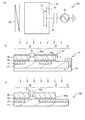
まず、本発明の実施例1の原理について説明する。図1(a)は誘導結合型プラズマ(Induced Coupled Plasma:ICP)エッチングを示す図である。図1(a)に示すように、プラズマエッチング装置20はチャンバー22、ステージ24、高周波電源25、キャパシタ26およびコイル28を備える。ステージ24は、チャンバー22内であって、コイル28と対向する位置に設けられている。ステージ24はキャパシタ26を介して高周波電源25に接続されている。ウェーハ10は、チャンバー22内のステージ24上に配置される。ウェーハ10は、例えば窒化物半導体層などの半導体層を含む。ウェーハ10は、図4(a)および図4(b)で後述する不活性化処理の実行後のものである。
First, the principle of the first embodiment of the present invention will be described. FIG. 1A is a diagram showing an inductively coupled plasma (ICP) etching. As shown in FIG. 1A, the
図1(b)は実施例1に係るウェーハ10を示す断面図である。図1(b)に示すように、ウェーハ10は、活性領域12および不活性領域14を含む。図1(b)に示すように、ウェーハ10のうち、半導体チップとなる領域(第1領域16)およびスクライブラインとなる領域(第2領域18)、および端部19において、ウェーハ10の下面から上面にかけて活性領域12が形成されている。第2領域18の活性領域と端部19の活性領域とは連続している。ウェーハ10のうち一部の領域の上面側に不活性領域14が形成されている。金属層30が、ウェーハ10の下面から上面の端部にかけて設けられている。金属層30は、活性領域12の上面、側面および下面に接触している。また、ウェーハ10の上面には、窒化シリコン(SiN)膜などの絶縁膜44が設けられ、絶縁膜44上にはレジスト46が設けられている。レジスト46は第1領域16上に開口部46aを有し、第2領域18上に開口部46bを有する。
FIG. 1B is a cross-sectional view illustrating the
図1(c)は比較例に係るウェーハ10Rを示す断面図である。ウェーハ10Rにおいては、第2領域18および端部19の上面側は不活性領域14である。また、金属層30はウェーハ10Rに設けられていない。
FIG. 1C is a cross-sectional view illustrating a
図1(a)に示したプラズマエッチング装置20を用いてプラズマエッチング処理を行う。チャンバー22内には例えばSF6ガスなどのエッチングガスが導入される。チャンバー22内の圧力は例えば0.1〜5Paである。コイル28に電流を流すことで発生する電界および磁界により、SF6ガスがプラズマ化する。高周波電源25のバイアスパワーは例えば10Wである。図1(b)および図1(c)に破線の矢印で示すように、イオンおよびラジカルをウェーハ10および10Rに衝突させることで、絶縁膜44のエッチングを行う。絶縁膜44を除去することにより、ウェーハ10および10Rの上面が露出する。
A plasma etching process is performed using the
図1(b)および図1(c)に示すように、プラズマエッチングが行われることで、絶縁膜44およびレジスト46の表面に正の電荷(チャージ)が蓄積する、いわゆるチャージアップが起こる。
As shown in FIGS. 1B and 1C, by performing the plasma etching, so-called charge-up, in which positive charges (charges) are accumulated on the surfaces of the insulating
図1(c)に示した比較例では、チャージアップにより、プラズマとウェーハ10Rとの間に電位差が生じ、電位差によって誘発されるプラズマからの電流がウェーハに流れる。図1(c)中に実線の矢印で示すように、チャージが第1領域16の活性領域12に集中するため、第1領域16の活性領域12に大きな電流A1が流れる。電流A1が流れることにより第1領域16の活性領域12にダメージが発生する。この結果、ウェーハ10Rに形成される電界効果トランジスタ(Field Effect Transistor:FET)などの半導体装置が劣化する。活性領域12のうちゲート電極直下のチャネル層などの半導体層(ゲート領域)にダメージが生じると、FETを駆動させた際のゲートリーク電流が増大する。また、プラズマエッチング工程などにおいてアーキングが発生し、ウェーハ10Rに形成されたキャパシタなどの受動素子またはFETなどが破損することもある。ウェーハ10Rに含まれる絶縁基板、およびGaNなどの窒化物半導体は高抵抗であるため、チャージはウェーハ10Rの表面に集中しやすく、特にウェーハの中心にたまりやすい。したがって、チャージアップに起因するダメージが発生しやすい。
In the comparative example shown in FIG. 1C, a potential difference is generated between the plasma and the
一方、図1(b)に示した実施例1では、プラズマエッチングにより、第1領域16および第2領域18の活性領域12が露出する。このため、実施例1において露出する活性領域12の面積が比較例よりも大きくなる。したがって、図1(b)中に実線の矢印で示すように、チャージが第1領域16および第2領域18両方の活性領域12に分散する。また、金属層30は活性領域12の下面、側面および上面に接触する。このため、チャージは、第2領域18および端部19の活性領域12を通じて金属層30に流れ込み、さらにウェーハ10の下面に流れる。
On the other hand, in Example 1 shown in FIG. 1B, the
これにより、ウェーハ10上面のチャージが除去される。この結果、ウェーハ10に流れる電流A1は、比較例より小さくなる。したがって、第1領域16の活性領域12のダメージが抑制される。活性領域12のゲート領域のダメージが抑制されることにより、FETを駆動させた際のリーク電流も低減する。また、アーキングも抑制される。後述の図5(a)に示すように、第2領域18の活性領域は第2領域18の延在方向に延在する。また図1(b)に示すように、活性領域12はウェーハ10の端部19において金属層30と接触している。このため、ウェーハ10の中央部のチャージが、第2領域18および端部19の活性領域12を通じて、金属層30に流れる。この結果、ウェーハ10の中央部におけるチャージの集中が抑制され、チャージアップによるダメージが抑制される。また、ウェーハ10全体がほぼ同一電位となるため、プラズマエッチングのエッチングレートがほぼ一定となる。この結果、安定したエッチングが可能となる。
Thereby, the charge on the upper surface of the
次に、ウェーハ10の層構造について説明する。図2(a)はウェーハ10を例示する平面図である。図2(b)はウェーハ10を例示する断面図である。図2(b)に示すように、ウェーハ10においては、下から基板32、チャネル層34、電子供給層36およびキャップ層38が積層されている。電子供給層36はチャネル層34の上面に接触している。基板32とチャネル層34との間にバッファ層が設けられていてもよい。
Next, the layer structure of the
基板32は例えばSiC(炭化シリコン)、Si(シリコン)またはサファイアなどにより形成されている。チャネル層34、電子供給層36、及びキャップ層38は、例えばエピタキシャル成長された窒化物半導体層である。チャネル層34は例えばi−GaN(ノンドープの窒化ガリウム)により形成されている。電子供給層36は、例えばAlGaN(窒化アルミニウムガリウム)により形成されている。キャップ層38は例えばGaNにより形成されている。
The
次に、実施例1に係る半導体装置の製造方法について、詳しく説明する。図3(a)はウェーハ10を例示する平面図である。図3(b)は図3(a)の線B−Bに沿った断面図である。図3(a)および図3(b)に示すように、蒸着法(真空蒸着法)またはスパッタリング法などにより、ウェーハ10の下面に向かって原料を照射することで、ウェーハ10に金属層30を形成する。蒸着法またはスパッタリング法などによれば、照射された原料は、図3(a)に示すように、ウェーハ10の下面のみならず、側面および上面の端部にまで連続して延在し、金属層30はウェーハ10を囲む。図3(b)に示すように、金属層30はウェーハ10の下面、側面、および上面の端部に接触する。金属層30は例えばウェーハ10に近い方からチタン/タングステン(Ti/W)を積層した膜であり、200nmの厚さを有する。
Next, a method for manufacturing the semiconductor device according to the first embodiment will be described in detail. FIG. 3A is a plan view illustrating the
図4(a)は第1領域16を例示する断面図である。図4(b)は第2領域18を例示する断面図である。図4(a)に示すように第1領域16における活性領域を活性領域12aと記載し、図4(b)に示すように第2領域18における活性領域を活性領域12bと記載することがある。図4(a)および図4(b)に示すように、ウェーハ10の上面にレジスト40を形成する。図4(a)に示すように、第1領域16の中央部はレジスト40に覆われ、周縁部はレジスト40から露出する。図4(b)に示すように、第2領域18の中央部はレジスト40に覆われ、周縁部はレジスト40から露出する。レジスト40を形成した後、例えば加速電圧30〜120keV、ドーズ量1〜5×10¹²/cm2で、アルゴン(Ar)イオンを注入することにより、ウェーハ10のレジスト40から露出した領域を不活性化する。図4(a)および図4(b)に示すように、キャップ層38、電子供給層36、およびチャネル層34の上側の一部が不活性領域14となる。第1領域16の中央部および第2領域18の中央部は不活性化されず、活性領域12aが残存する。スクライブラインの幅方向において第2領域18の中央部が活性領域12b、端部が不活性領域14となる。不活性化処理の後、レジスト40を除去する。
FIG. 4A is a cross-sectional view illustrating the
図5(a)はウェーハ10を例示する平面図である。図5(b)はウェーハ10の端部付近を拡大した平面図である。図5(c)は図5(b)の線C−Cに沿った断面図である。図6はウェーハ10のうち1つの半導体チップとなる部分を拡大した平面図である。図5(a)、図5(b)および図6に示すように、第1領域16の活性領域12aは不活性領域14に囲まれる。不活性領域14は第2領域18の活性領域12bに囲まれる。図5(a)から図5(c)に示すように、複数の活性領域12aの間は、活性領域12bおよび不活性領域14により分離される。また、図5(c)に示すように、ウェーハ10の端部19は金属層30に覆われているため、Arイオンから保護され、不活性化されない。したがって、ウェーハ10の端部に活性領域12(活性領域12cとする)が残存し、金属層30と接触する。また図5(b)に示すように活性領域12bは第2領域18の延在方向に延在しており、図5(c)に示すように端部19の活性領域12cと連続し、電気的に接続されている。
FIG. 5A is a plan view illustrating the
図7(a)は第1領域16を例示する断面図である。図7(b)は第2領域18を例示する断面図である。図7(a)に示すように、例えば蒸着・リフトオフ法により、第1領域16のキャップ層38の上面に、例えば2つのオーミック電極42を形成する。その後、例えば600℃で熱処理を行うことで、活性領域12aとオーミック電極42との間でオーミック接触を形成する。2つのオーミック電極42のうち一方はソース電極、他方はドレイン電極として機能する。オーミック電極42は、例えばキャップ層に近い方から順にタンタル/アルミニウム/タンタル(Ta/Al/Ta)などの金属を積層した、厚さ300〜500nmの電極である。図7(b)に示すように、オーミック電極42は第2領域18には形成されない。
FIG. 7A is a cross-sectional view illustrating the
図8(a)は第1領域16を例示する断面図である。図8(b)は第2領域18を例示する断面図である。図8(a)および図8(b)に示すように、例えばプラズマCVD(Chemical Vapor Deposition)法または原子層堆積(Atomic Layer Deposition:ALD)法などにより、ウェーハ10の上面に絶縁膜44を形成する。絶縁膜44は、例えば厚さ50〜100nmのSiNなどの絶縁体により形成されている。
FIG. 8A is a cross-sectional view illustrating the
図9(a)は第1領域16を例示する断面図である。図9(b)は第2領域18を例示する断面図である。図9(a)および図9(b)に示すように、絶縁膜44の上にレジスト46を形成する。図9(a)に示すように、レジスト46は第1領域16のキャップ層38の上に開口部46aを有する。図9(b)に示すように、レジスト46は第2領域18のキャップ層38の上に開口部46bを有する。開口部46aおよび46bからは絶縁膜44が露出する。
FIG. 9A is a cross-sectional view illustrating the
図10(a)は第1領域16を例示する断面図であり、図11の線D−Dに沿った断面図である。図10(b)は第2領域18を例示する断面図である。図11はウェーハ10のうち1つの半導体チップとなる部分を拡大した平面図である。図10(a)、図10(b)および図11に示すように、レジスト46の開口部46aおよび46bから露出する絶縁膜44を、プラズマエッチングにより除去する。図10(a)および図11に示すように、プラズマエッチングにより、絶縁膜44に開口部44aが形成される。開口部44aはゲート窓であり、活性領域12aの一部(ゲート領域)が開口部44aから露出する。図10(b)および図11に示すように、プラズマエッチングにより、絶縁膜44に開口部44bが形成され、活性領域12bが開口部44bから露出する。また図11に示すように、ソースパッドおよびドレインパッドの設けられる領域には開口部44cが形成される。なお、開口部44cは設けなくてもよい。プラズマエッチングには、例えば図1(a)に示したプラズマエッチング装置20を用いる。プラズマエッチングは例えばエッチングガスにSF6ガス、圧力0.1〜5Pa、バイアスパワー10Wの条件で実施する。金属層30はプラズマエッチング装置20の接地電位に接続する。プラズマエッチングの後、レジスト46を除去する。
FIG. 10A is a cross-sectional view illustrating the
プラズマエッチングにより、ウェーハ10の表面がチャージアップする。図1(b)において説明したように、チャージは第1領域16および第2領域18の活性領域12に分散する。第2領域18の活性領域12bはウェーハ10の端部まで延在し、端部19の活性領域12cと連続している。金属層30はウェーハ10の端部において活性領域12cと接触している。ウェーハ10の下面の金属層30はプラズマエッチング装置20の接地電位に接続されるため、チャージは第2領域18を通じて金属層30に流れ、ウェーハ10の裏面側に流れ込む。したがって、チャージはウェーハ10の上面から除去される。この結果、チャージアップに起因する第1領域16の活性領域12aのダメージが抑制される。第1領域16の活性領域12aのうちゲート電極の直下となるチャネル層34など半導体層のダメージが抑制されるため、リーク電流が低減する。
The surface of the
ウェーハ10の基板32が例えばSiCまたはサファイアなどにより形成された絶縁基板の場合、ウェーハ10の表面はチャージアップしやすい。また、ウェーハ10に含まれる半導体がGaNのような窒化物半導体の場合、ウェーハ10の表面はチャージアップしやすい。実施例1によれば、ウェーハ10が絶縁基板および窒化物半導体を含んでいる場合でも、チャージを除去することができる。この結果、チャージアップに起因するダメージを抑制することができる。
When the
図12(a)は第1領域16を例示する断面図である。図12(b)は第2領域18を例示する断面図である。図12(a)に示すように、例えば蒸着・リフトオフ法により、プラズマエッチングにより露出した第1領域16のキャップ層38の上面に、ゲート電極48を形成する。ゲート電極48は、キャップ層38に近い方から順にニッケル/パラジウム/金(Ni/Pd/Au)を積層して形成されており、厚さは例えば300〜600nmである。図12(b)に示すように、ゲート電極48は、第2領域18には形成されない。
FIG. 12A is a cross-sectional view illustrating the
図13(a)は第1領域16を例示する断面図である。図13(b)は第2領域18を例示する断面図である。図13(a)および図13(b)に示すように、例えばプラズマCVD法またはALD法などにより、絶縁膜50を形成する。図13(a)に示すように、絶縁膜50は絶縁膜44およびゲート電極48を覆う。図13(b)に示すように、絶縁膜50は第2領域18におけるキャップ層38を覆う。絶縁膜50は、例えば厚さ50〜400nmのSiNなどの絶縁体により形成されている。
FIG. 13A is a cross-sectional view illustrating the
図14(a)は第1領域16を例示する断面図である。図14(b)は第2領域18を例示する断面図である。図14(a)および図14(b)に示すように、絶縁膜50の上にレジスト52を形成する。図14(a)に示すように、レジスト52は第1領域16において、オーミック電極42の上に開口部52aを有する。図14(b)に示すように、レジスト52は第2領域18の絶縁膜50の上に開口部52bを有する。開口部52aおよび52bからは絶縁膜50が露出する。
FIG. 14A is a cross-sectional view illustrating the
図15(a)は第1領域16を例示する断面図であり、図16の線E−Eに沿った断面図である。図15(b)は第2領域18を例示する断面図である。図16はウェーハ10のうち1つの半導体チップとなる部分を拡大した平面図である。図15(a)、図15(b)および図16に示すように、プラズマエッチングを行い、レジスト52の開口部52aおよび52bから露出する絶縁膜50を除去する。図15(a)および図16に示すように、プラズマエッチングにより、絶縁膜44および50に開口部51が形成され、オーミック電極42の表面が開口部51から露出する。図15(b)および図16に示すように、プラズマエッチングにより、絶縁膜44および50に開口部53が形成され、活性領域12bが開口部53から露出する。また図16に示すように、ゲートパッド、ソースパッドおよびドレインパッドの設けられる領域には開口部55が形成される。プラズマエッチングには、例えば図1(a)に示したプラズマエッチング装置20を用いる。プラズマエッチングは例えばエッチングガスにSF6ガス、圧力0.1〜5Pa、バイアスパワー10Wの条件で実施する。
FIG. 15A is a cross-sectional view illustrating the
プラズマエッチングにより、ウェーハ10の表面がチャージアップする。図1(b)において説明したものと同様の原理により、チャージは第1領域16および第2領域18の活性領域に分散し、第2領域18を通じて金属層30に流れ、ウェーハ10の裏面側に流れ込む。したがって、チャージはウェーハ10の上面から除去される。この結果、チャージアップに起因するウェーハ10のダメージが抑制される。
The surface of the
図17(a)は第1領域16を例示する断面図である。図17(b)は第2領域18を例示する断面図である。図17(a)に示すように、例えば電解メッキ法により、オーミック電極42の上面に配線層54を形成する。具体的には、オーミック電極42および絶縁膜50の上にシードメタル(不図示)を設け、シードメタルに電流を流すことで、配線層54を形成する。配線層54は例えば厚さ1〜5μmのAuにより形成され、オーミック電極42と電気的に接続されている。配線層54の形成後、シードメタルは、例えばエッチングなどにより除去する。また、図17(b)に示すように、配線層54は第2領域18には形成されない。
FIG. 17A is a cross-sectional view illustrating the
図18(a)はウェーハ10を例示する断面図である。図18(b)は半導体チップ60を例示する断面図である。図18(a)に示すように、複数の第1領域16の間には第2領域18が位置する。図18(b)に示すように、ブレード62を用いて、第2領域18をスクライブラインとして、ウェーハ10を切断する。これにより、ウェーハ10を個片化し、複数の半導体チップ60を形成する。図18(a)に示すように、第2領域18の中央部は活性領域12bである。またスクライブラインの幅W1(例えば100μm)は、活性領域12bの幅W2(例えば80μm)より大きい。このため、第2領域18の活性領域12bはダイシングにより除去される。したがって、半導体チップ60の端部は不活性領域14となる。これにより、例えばゲートパッドなどに接続されるワイヤが半導体チップ60の端部に接触しても、ワイヤと活性領域12とのショートが抑制される。
FIG. 18A is a cross-sectional view illustrating the
次に、実施例1に係る製造方法により製造された半導体チップ60と、比較例に係る製造方法により製造された半導体チップとにおける、リーク電流の測定結果について説明する。図1(c)に示したように、比較例では、第2領域18および端部19が不活性領域14であり、かつ金属層30がウェーハ10Rに設けられていない。他の処理は、実施例1と同じである。ここでは、半導体チップのFETにおけるゲート・ドレイン間の逆方向2端子ゲートリーク電流(以下、リーク電流)を比較している。FETの基板32はSiC、チャネル層34はGaN、電子供給層36はAlGaN、キャップ層38はGaNにより形成されている。
Next, the measurement results of the leak current of the
図19はリーク電流の測定結果を示す図である。横軸はドレイン・ソース間電圧Vds、縦軸はリーク電流Igを示す。実線は実施例1、破線は比較例の実験結果を示す。 FIG. 19 is a diagram showing the measurement results of the leak current. The horizontal axis shows the drain-source voltage Vds, and the vertical axis shows the leak current Ig. The solid line shows the experimental result of Example 1 and the broken line shows the experimental result of Comparative Example.
図19に示すように、実施例1および比較例の両方において、ドレイン・ソース間電圧Vdsの上昇と共に、リーク電流は上昇する。実施例1におけるリーク電流は、比較例におけるリーク電流の1000分の1程度である。 As shown in FIG. 19, in both the example 1 and the comparative example, the leak current increases as the drain-source voltage Vds increases. The leak current in Example 1 is about 1/1000 of the leak current in Comparative Example.
比較例においては、チャージが第1領域16の活性領域に集中する。このため、第1領域16のゲート電極付近の部分に大きなダメージが生じる。これによりリーク電流が増大する。
In the comparative example, the charge concentrates on the active region of the
一方、実施例1によれば、第2領域18に活性領域12bが残存し、ウェーハ10の端部の活性領域12cは金属層30に接触する。このため、プラズマエッチングにおいて発生するチャージを、第2領域18を通じて、金属層30に逃がすことができる。これにより、チャージアップに起因する第1領域16の活性領域12aのダメージを抑制することができる。図10(a)に示したように、絶縁膜44に開口部44a(ゲート窓)を設ける際、活性領域12a、特にゲート電極48直下の領域(ゲート領域)のダメージが抑制される。この結果、図19に示したように、半導体チップ60のFETにおけるリーク電流を大幅に低減することができる。また、アーキングによる破損を抑制することもできる。
On the other hand, according to the first embodiment, the
スクライブライン(第2領域18)には、スクライブラインの延在方向に延在する活性領域12bが形成される。スクライブラインの幅W1は変更することができるが、活性領域12bの幅W2より大きいことが好ましい。また、スクライブラインの幅方向において第2領域18の中央部は活性領域12bであり、端部は不活性領域14であることが好ましい。これにより、活性領域12bがダイシングにより除去され、半導体チップ60の端部が不活性領域14となるためである。この結果、例えばワイヤなどが半導体チップ60の端部に接触しても、活性領域12とワイヤとのショートは抑制される。また、第2領域18の少なくとも一部が活性領域12bであればよい。例えば、第2領域18の全体が活性領域12bである場合、ダイシングにより活性領域12bの全てを除去することが好ましい。
金属層30は、蒸着法またはスパッタリング法によりウェーハ10の下面に原料を照射することで形成される。これによりウェーハ10の下面から、側面および上面の端部にかけて金属層30が形成される。金属層30はプラズマエッチング装置20の接地電位に接続することが好ましい。プラズマエッチングにより発生したチャージが金属層30に流れやすくなる。また、金属層30はウェーハ10の外周を囲む。特に、図3(a)および図3(b)に示すように、金属層30はウェーハ10の外周を完全に囲むことが好ましい。これにより、チャージはウェーハ10の平面内の各方向に流れ、効率的に除去される。アルゴンのイオン注入以外にウェーハ10に活性領域12または不活性領域14を形成する工程を行ってもよい。これによりスクライブライン(第2領域18)および端部19に活性領域が形成されればよい。
The
図10(a)および図10(b)に示した絶縁膜44のプラズマエッチング、ならびに図15(a)および図15(b)に示した絶縁膜50のプラズマエッチングの両方において、活性領域12bが露出する。このため、2回のプラズマエッチングにおいて発生するチャージが除去される。プラズマエッチングを3回以上行う場合でも、活性領域12bを露出させることで、活性領域12bを通じてチャージを金属層30に逃がすことができる。また、例えばプラズマアッシングおよびプラズマCVDなど、プラズマを用いるエッチング以外の工程において発生するチャージを除去することもできる。特に図10(a)から図11に示したように、活性領域12aが露出する工程においては、活性領域12bも露出することが好ましい。これにより、チャージが活性領域12aおよび12bに分散し、ダメージを効果的に抑制することができる。
In both the plasma etching of the insulating
実施例1において、半導体チップ60はFETを含むとしたが、例えばFET以外のトランジスタ、またはトランジスタ以外を含んでもよい。半導体チップ60は複数のFETを含んでもよい。一枚のウェーハ10から得られる半導体チップ60の数はいくつでもよい。スクライブライン(第2領域18)中の活性領域12bが大きくなるほど、チャージが活性領域12bに分散し、金属層30に流れやすくなる。したがって、一枚のウェーハ10から得られる半導体チップ60の数を増やすことで、スクライブラインの本数を増やし、チャージを効果的に除去することができる。
In the first embodiment, the
ウェーハ10は化合物半導体を含む。化合物半導体は、例えば砒素系半導体および窒化物半導体などを含む。砒素系半導体とはガリウム砒素(GaAs)など砒素(As)を含む半導体である。窒化物半導体とは、窒素(N)を含む半導体であり、例えば窒化ガリウム(GaN)、窒化アルミニウムガリウム(AlGaN)、窒化インジウムガリウム(InGaN)、窒化インジウム(InN)、および窒化アルミニウムインジウムガリウム(AlInGaN)などがある。なお、ウェーハ10は、FET以外のトランジスタ、およびトランジスタ以外の半導体素子を含んでもよい。絶縁膜44および50は、SiN以外に酸化シリコン(SiO2)、窒化酸化シリコン(SiON)により形成されてもよい。
The
以上、本発明の実施例について詳述したが、本発明はかかる特定の実施例に限定されるものではなく、特許請求の範囲に記載された本発明の要旨の範囲内において、種々の変形・変更が可能である。 As described above, the embodiments of the present invention have been described in detail. However, the present invention is not limited to the specific embodiments, and various modifications and changes may be made within the scope of the present invention described in the appended claims. Changes are possible.
10 ウェーハ
12、12a、12b、12c 活性領域
14 不活性領域
16 第1領域
18 第2領域
19 端部
20 プラズマエッチング装置
22 チャンバー
24 ステージ
25 高周波電源
26 キャパシタ
28 コイル
30 金属層
32 基板
34 チャネル層
36 電子供給層
38 キャップ層
40、46、52 レジスト
42 オーミック電極
44、50 絶縁膜
44a、44b、46a、46b、50a、50b、51、52a、52b、
53、55 開口部
48 ゲート電極
54 配線層
60 半導体チップ
DESCRIPTION OF
53, 55
Claims (5)
当該ウェーハの下面と当該ウェーハの端部における当該活性領域とを電気的に接続する第1金属層を形成する工程と、
当該複数の半導体チップそれぞれの周辺領域、および当該複数のスクライブラインの周辺領域それぞれにおける当該活性領域を不活性化する工程と、
当該ウェーハの上面に絶縁膜を形成する工程と、
当該半導体チップそれぞれの当該周辺領域以外の領域である第1領域の当該絶縁膜、およびそれぞれの当該スクライブラインの当該周辺領域以外の領域の当該絶縁膜にプラズマエッチングにより同時に開口を形成する工程と、を含み、
前記不活性化する工程において、前記複数の半導体チップそれぞれの前記第1領域、および前記ウェーハの端部に前記活性領域が残存し、
前記第1領域における前記活性領域は前記ウェーハの端部における前記活性領域に電気的に接続される半導体装置の製造方法。 A method of manufacturing a semiconductor device having an upper surface and a lower surface opposite to the upper surface, and obtaining a plurality of semiconductor chips partitioned by a plurality of scribe lines from a wafer including an active region over the entire upper surface,
Forming a first metal layer that electrically connects the lower surface of the wafer and the active region at the edge of the wafer;
Deactivating the active region in each of the peripheral regions of the plurality of semiconductor chips, and the peripheral regions of the plurality of scribe lines,
Forming an insulating film on the upper surface of the wafer,
Simultaneously forming an opening by plasma etching in the insulating film in the first region , which is a region other than the peripheral region of each semiconductor chip, and in the insulating film in a region other than the peripheral region of each scribe line; only including,
In the step of inactivating, the first region of each of the plurality of semiconductor chips, and the active region remains at the end of the wafer,
The method of manufacturing a semiconductor device, wherein the active region in the first region is electrically connected to the active region at an edge of the wafer .
当該切断する工程は、当該それぞれのスクライブラインにおける当該活性領域を除去する請求項1〜4のいずれか一項に記載の半導体装置の製造方法。 Including cutting the wafer along the respective scribe lines,
The method of manufacturing a semiconductor device according to claim 1, wherein the cutting step removes the active region in each of the scribe lines.
Priority Applications (2)
| Application Number | Priority Date | Filing Date | Title |
|---|---|---|---|
| JP2015224110A JP6631782B2 (en) | 2015-11-16 | 2015-11-16 | Method for manufacturing semiconductor device |
| US15/352,811 US9960043B2 (en) | 2015-11-16 | 2016-11-16 | Process of forming semiconductor device |
Applications Claiming Priority (1)
| Application Number | Priority Date | Filing Date | Title |
|---|---|---|---|
| JP2015224110A JP6631782B2 (en) | 2015-11-16 | 2015-11-16 | Method for manufacturing semiconductor device |
Publications (3)
| Publication Number | Publication Date |
|---|---|
| JP2017092384A JP2017092384A (en) | 2017-05-25 |
| JP2017092384A5 JP2017092384A5 (en) | 2018-09-13 |
| JP6631782B2 true JP6631782B2 (en) | 2020-01-15 |
Family
ID=58691993
Family Applications (1)
| Application Number | Title | Priority Date | Filing Date |
|---|---|---|---|
| JP2015224110A Active JP6631782B2 (en) | 2015-11-16 | 2015-11-16 | Method for manufacturing semiconductor device |
Country Status (2)
| Country | Link |
|---|---|
| US (1) | US9960043B2 (en) |
| JP (1) | JP6631782B2 (en) |
Families Citing this family (4)
| Publication number | Priority date | Publication date | Assignee | Title |
|---|---|---|---|---|
| JP6631782B2 (en) * | 2015-11-16 | 2020-01-15 | 住友電工デバイス・イノベーション株式会社 | Method for manufacturing semiconductor device |
| JPWO2018207736A1 (en) | 2017-05-08 | 2020-05-28 | 国立大学法人京都大学 | Method for introducing polynucleotide into male germ cell or sertoli cell |
| JP7303215B2 (en) * | 2018-10-31 | 2023-07-04 | ソニーセミコンダクタソリューションズ株式会社 | Semiconductor device, communication module, and method for manufacturing semiconductor device |
| US20220392856A1 (en) * | 2021-06-03 | 2022-12-08 | Nxp Usa, Inc. | Wafer with semiconductor devices and integrated electrostatic discharge protection |
Family Cites Families (11)
| Publication number | Priority date | Publication date | Assignee | Title |
|---|---|---|---|---|
| US5874747A (en) * | 1996-02-05 | 1999-02-23 | Advanced Technology Materials, Inc. | High brightness electroluminescent device emitting in the green to ultraviolet spectrum and method of making the same |
| JPH1079392A (en) | 1996-09-04 | 1998-03-24 | Mitsubishi Electric Corp | Manufacture of wiring layer of semiconductor device |
| US8294172B2 (en) * | 2002-04-09 | 2012-10-23 | Lg Electronics Inc. | Method of fabricating vertical devices using a metal support film |
| US9136173B2 (en) * | 2012-11-07 | 2015-09-15 | Semiconductor Components Industries, Llc | Singulation method for semiconductor die having a layer of material along one major surface |
| US9484316B2 (en) * | 2013-11-01 | 2016-11-01 | Infineon Technologies Ag | Semiconductor devices and methods of forming thereof |
| JP6442800B2 (en) * | 2014-12-25 | 2018-12-26 | 住友電工デバイス・イノベーション株式会社 | Semiconductor device and method of manufacturing the semiconductor device |
| JP6631782B2 (en) * | 2015-11-16 | 2020-01-15 | 住友電工デバイス・イノベーション株式会社 | Method for manufacturing semiconductor device |
| US10249506B2 (en) * | 2016-03-03 | 2019-04-02 | Gan Systems Inc. | GaN-on-si semiconductor device structures for high current/ high voltage lateral GaN transistors and methods of fabrication thereof |
| US10283501B2 (en) * | 2016-03-03 | 2019-05-07 | Gan Systems Inc. | GaN-on-Si semiconductor device structures for high current/ high voltage lateral GaN transistors and methods of fabrication thereof |
| JP6524534B2 (en) * | 2016-03-09 | 2019-06-05 | パナソニックIpマネジメント株式会社 | Method of manufacturing element chip |
| US10366923B2 (en) * | 2016-06-02 | 2019-07-30 | Semiconductor Components Industries, Llc | Method of separating electronic devices having a back layer and apparatus |
-
2015
- 2015-11-16 JP JP2015224110A patent/JP6631782B2/en active Active
-
2016
- 2016-11-16 US US15/352,811 patent/US9960043B2/en active Active
Also Published As
| Publication number | Publication date |
|---|---|
| US20170140939A1 (en) | 2017-05-18 |
| US9960043B2 (en) | 2018-05-01 |
| JP2017092384A (en) | 2017-05-25 |
Similar Documents
| Publication | Publication Date | Title |
|---|---|---|
| US11152499B2 (en) | Nitride semiconductor device and method for manufacturing same | |
| JP5970736B2 (en) | Manufacturing method of semiconductor device | |
| TWI767726B (en) | IMPROVED GaN STRUCTURES | |
| JP5662367B2 (en) | Nitride semiconductor device and manufacturing method thereof | |
| US9577064B2 (en) | High electron mobility transistors with field plate electrode | |
| JP6631782B2 (en) | Method for manufacturing semiconductor device | |
| EP2601678B1 (en) | Manufacturing of scalable gate length high electron mobility transistors | |
| US20130256755A1 (en) | Semiconductor device and method for manufacturing the same | |
| US9299770B2 (en) | Method for manufacturing semiconductor device | |
| TWI676293B (en) | Semiconductor devices and methods for forming same | |
| JP5740356B2 (en) | Semiconductor device | |
| JP6171250B2 (en) | Semiconductor device | |
| JP2012033689A (en) | Manufacturing method of semiconductor device | |
| US20140120718A1 (en) | Method of fabricating semiconductor device | |
| US20140299946A1 (en) | Semiconductor device | |
| CN105308721A (en) | Method to fabricate self-aligned isolation in gallium nitride devices and integrated circuits | |
| JP2010278150A (en) | Compound semiconductor device and method of manufacturing the same | |
| US11171005B2 (en) | Semiconductor device manufacturing method | |
| JP6048732B2 (en) | Semiconductor device and manufacturing method thereof | |
| JP6052977B2 (en) | Semiconductor device and manufacturing method thereof | |
| US20230053074A1 (en) | Semiconductor device and manufacturing method thereof | |
| JP5991790B2 (en) | Manufacturing method of semiconductor device | |
| JP6029060B2 (en) | Semiconductor device | |
| JP6776501B2 (en) | Manufacturing method of semiconductor devices | |
| US20220392856A1 (en) | Wafer with semiconductor devices and integrated electrostatic discharge protection |
Legal Events
| Date | Code | Title | Description |
|---|---|---|---|
| A521 | Request for written amendment filed |
Free format text: JAPANESE INTERMEDIATE CODE: A523 Effective date: 20180802 |
|
| A621 | Written request for application examination |
Free format text: JAPANESE INTERMEDIATE CODE: A621 Effective date: 20180802 |
|
| A977 | Report on retrieval |
Free format text: JAPANESE INTERMEDIATE CODE: A971007 Effective date: 20190411 |
|
| A131 | Notification of reasons for refusal |
Free format text: JAPANESE INTERMEDIATE CODE: A131 Effective date: 20190604 |
|
| A521 | Request for written amendment filed |
Free format text: JAPANESE INTERMEDIATE CODE: A523 Effective date: 20190719 |
|
| TRDD | Decision of grant or rejection written | ||
| A01 | Written decision to grant a patent or to grant a registration (utility model) |
Free format text: JAPANESE INTERMEDIATE CODE: A01 Effective date: 20191112 |
|
| A61 | First payment of annual fees (during grant procedure) |
Free format text: JAPANESE INTERMEDIATE CODE: A61 Effective date: 20191126 |
|
| R150 | Certificate of patent or registration of utility model |
Ref document number: 6631782 Country of ref document: JP Free format text: JAPANESE INTERMEDIATE CODE: R150 |
|
| R250 | Receipt of annual fees |
Free format text: JAPANESE INTERMEDIATE CODE: R250 |
|
| R250 | Receipt of annual fees |
Free format text: JAPANESE INTERMEDIATE CODE: R250 |