CN101350367B - Liquid crystal display device - Google Patents
Liquid crystal display device Download PDFInfo
- Publication number
- CN101350367B CN101350367B CN2008101339953A CN200810133995A CN101350367B CN 101350367 B CN101350367 B CN 101350367B CN 2008101339953 A CN2008101339953 A CN 2008101339953A CN 200810133995 A CN200810133995 A CN 200810133995A CN 101350367 B CN101350367 B CN 101350367B
- Authority
- CN
- China
- Prior art keywords
- semiconductor film
- liquid crystal
- film
- electrode
- cushion
- Prior art date
- Legal status (The legal status is an assumption and is not a legal conclusion. Google has not performed a legal analysis and makes no representation as to the accuracy of the status listed.)
- Expired - Fee Related
Links
- 239000004973 liquid crystal related substance Substances 0.000 title claims abstract description 163
- 239000004065 semiconductor Substances 0.000 claims abstract description 243
- 230000015572 biosynthetic process Effects 0.000 claims abstract description 60
- 239000011241 protective layer Substances 0.000 claims abstract description 40
- IJGRMHOSHXDMSA-UHFFFAOYSA-N Atomic nitrogen Chemical compound N#N IJGRMHOSHXDMSA-UHFFFAOYSA-N 0.000 claims description 60
- 239000001257 hydrogen Substances 0.000 claims description 34
- 229910052739 hydrogen Inorganic materials 0.000 claims description 34
- UFHFLCQGNIYNRP-UHFFFAOYSA-N Hydrogen Chemical compound [H][H] UFHFLCQGNIYNRP-UHFFFAOYSA-N 0.000 claims description 30
- 229910052757 nitrogen Inorganic materials 0.000 claims description 30
- QVGXLLKOCUKJST-UHFFFAOYSA-N atomic oxygen Chemical group [O] QVGXLLKOCUKJST-UHFFFAOYSA-N 0.000 claims description 21
- 239000011737 fluorine Substances 0.000 claims description 14
- 229910052731 fluorine Inorganic materials 0.000 claims description 14
- OKTJSMMVPCPJKN-UHFFFAOYSA-N Carbon Chemical compound [C] OKTJSMMVPCPJKN-UHFFFAOYSA-N 0.000 claims description 9
- 229910052799 carbon Inorganic materials 0.000 claims description 9
- 239000000460 chlorine Substances 0.000 claims description 9
- ZCYVEMRRCGMTRW-UHFFFAOYSA-N 7553-56-2 Chemical compound [I] ZCYVEMRRCGMTRW-UHFFFAOYSA-N 0.000 claims description 6
- WKBOTKDWSSQWDR-UHFFFAOYSA-N Bromine atom Chemical compound [Br] WKBOTKDWSSQWDR-UHFFFAOYSA-N 0.000 claims description 6
- ZAMOUSCENKQFHK-UHFFFAOYSA-N Chlorine atom Chemical compound [Cl] ZAMOUSCENKQFHK-UHFFFAOYSA-N 0.000 claims description 6
- GDTBXPJZTBHREO-UHFFFAOYSA-N bromine Substances BrBr GDTBXPJZTBHREO-UHFFFAOYSA-N 0.000 claims description 6
- 229910052794 bromium Inorganic materials 0.000 claims description 6
- 229910052801 chlorine Inorganic materials 0.000 claims description 6
- 239000011630 iodine Substances 0.000 claims description 6
- 229910052740 iodine Inorganic materials 0.000 claims description 6
- PXGOKWXKJXAPGV-UHFFFAOYSA-N Fluorine Chemical compound FF PXGOKWXKJXAPGV-UHFFFAOYSA-N 0.000 claims 2
- 239000010408 film Substances 0.000 abstract description 502
- 239000010409 thin film Substances 0.000 abstract description 120
- 239000010410 layer Substances 0.000 abstract description 24
- 239000000758 substrate Substances 0.000 description 104
- 238000000034 method Methods 0.000 description 75
- 238000006243 chemical reaction Methods 0.000 description 64
- 238000005755 formation reaction Methods 0.000 description 54
- 239000012535 impurity Substances 0.000 description 38
- 238000005530 etching Methods 0.000 description 32
- 230000008569 process Effects 0.000 description 30
- 238000012545 processing Methods 0.000 description 30
- 238000005268 plasma chemical vapour deposition Methods 0.000 description 29
- BLRPTPMANUNPDV-UHFFFAOYSA-N Silane Chemical compound [SiH4] BLRPTPMANUNPDV-UHFFFAOYSA-N 0.000 description 28
- 239000013078 crystal Substances 0.000 description 25
- 229910000077 silane Inorganic materials 0.000 description 25
- 230000000052 comparative effect Effects 0.000 description 23
- 210000002858 crystal cell Anatomy 0.000 description 23
- 229910052710 silicon Inorganic materials 0.000 description 23
- 239000010703 silicon Substances 0.000 description 23
- XUIMIQQOPSSXEZ-UHFFFAOYSA-N Silicon Chemical compound [Si] XUIMIQQOPSSXEZ-UHFFFAOYSA-N 0.000 description 22
- 239000007789 gas Substances 0.000 description 22
- 238000004519 manufacturing process Methods 0.000 description 22
- 229910052581 Si3N4 Inorganic materials 0.000 description 21
- 238000011010 flushing procedure Methods 0.000 description 19
- 239000001301 oxygen Substances 0.000 description 19
- 229910052760 oxygen Inorganic materials 0.000 description 19
- 125000004429 atom Chemical group 0.000 description 17
- 230000005684 electric field Effects 0.000 description 17
- HQVNEWCFYHHQES-UHFFFAOYSA-N silicon nitride Chemical compound N12[Si]34N5[Si]62N3[Si]51N64 HQVNEWCFYHHQES-UHFFFAOYSA-N 0.000 description 14
- YCKRFDGAMUMZLT-UHFFFAOYSA-N Fluorine atom Chemical compound [F] YCKRFDGAMUMZLT-UHFFFAOYSA-N 0.000 description 12
- 238000003475 lamination Methods 0.000 description 12
- 229910021417 amorphous silicon Inorganic materials 0.000 description 11
- 230000000694 effects Effects 0.000 description 10
- 229910052751 metal Inorganic materials 0.000 description 10
- 239000002184 metal Substances 0.000 description 10
- 125000006850 spacer group Chemical group 0.000 description 10
- 238000004040 coloring Methods 0.000 description 9
- 239000012467 final product Substances 0.000 description 9
- XKRFYHLGVUSROY-UHFFFAOYSA-N Argon Chemical compound [Ar] XKRFYHLGVUSROY-UHFFFAOYSA-N 0.000 description 8
- ZOKXTWBITQBERF-UHFFFAOYSA-N Molybdenum Chemical compound [Mo] ZOKXTWBITQBERF-UHFFFAOYSA-N 0.000 description 8
- 229910052782 aluminium Inorganic materials 0.000 description 8
- XAGFODPZIPBFFR-UHFFFAOYSA-N aluminium Chemical compound [Al] XAGFODPZIPBFFR-UHFFFAOYSA-N 0.000 description 8
- 239000000463 material Substances 0.000 description 8
- 239000011733 molybdenum Substances 0.000 description 8
- 229910052750 molybdenum Inorganic materials 0.000 description 8
- OBNDGIHQAIXEAO-UHFFFAOYSA-N [O].[Si] Chemical compound [O].[Si] OBNDGIHQAIXEAO-UHFFFAOYSA-N 0.000 description 7
- 238000004140 cleaning Methods 0.000 description 7
- 230000014509 gene expression Effects 0.000 description 7
- 150000002367 halogens Chemical class 0.000 description 7
- 238000010438 heat treatment Methods 0.000 description 7
- 239000012528 membrane Substances 0.000 description 7
- 230000003647 oxidation Effects 0.000 description 7
- 238000007254 oxidation reaction Methods 0.000 description 7
- 238000011282 treatment Methods 0.000 description 7
- RYGMFSIKBFXOCR-UHFFFAOYSA-N Copper Chemical compound [Cu] RYGMFSIKBFXOCR-UHFFFAOYSA-N 0.000 description 6
- 239000004411 aluminium Substances 0.000 description 6
- 239000004568 cement Substances 0.000 description 6
- 239000002131 composite material Substances 0.000 description 6
- 229910052802 copper Inorganic materials 0.000 description 6
- 239000010949 copper Substances 0.000 description 6
- 229910052736 halogen Inorganic materials 0.000 description 6
- 150000004767 nitrides Chemical class 0.000 description 6
- 238000004544 sputter deposition Methods 0.000 description 6
- 230000000007 visual effect Effects 0.000 description 6
- RTAQQCXQSZGOHL-UHFFFAOYSA-N Titanium Chemical compound [Ti] RTAQQCXQSZGOHL-UHFFFAOYSA-N 0.000 description 5
- 229920001940 conductive polymer Polymers 0.000 description 5
- 238000002425 crystallisation Methods 0.000 description 5
- 230000008025 crystallization Effects 0.000 description 5
- 239000011521 glass Substances 0.000 description 5
- 230000002262 irrigation Effects 0.000 description 5
- 238000003973 irrigation Methods 0.000 description 5
- 239000013081 microcrystal Substances 0.000 description 5
- 239000000203 mixture Substances 0.000 description 5
- 230000009467 reduction Effects 0.000 description 5
- 229910052715 tantalum Inorganic materials 0.000 description 5
- GUVRBAGPIYLISA-UHFFFAOYSA-N tantalum atom Chemical compound [Ta] GUVRBAGPIYLISA-UHFFFAOYSA-N 0.000 description 5
- 239000010936 titanium Substances 0.000 description 5
- 229910052719 titanium Inorganic materials 0.000 description 5
- QGZKDVFQNNGYKY-UHFFFAOYSA-N Ammonia Chemical compound N QGZKDVFQNNGYKY-UHFFFAOYSA-N 0.000 description 4
- VYPSYNLAJGMNEJ-UHFFFAOYSA-N Silicium dioxide Chemical compound O=[Si]=O VYPSYNLAJGMNEJ-UHFFFAOYSA-N 0.000 description 4
- GWEVSGVZZGPLCZ-UHFFFAOYSA-N Titan oxide Chemical compound O=[Ti]=O GWEVSGVZZGPLCZ-UHFFFAOYSA-N 0.000 description 4
- 229910052786 argon Inorganic materials 0.000 description 4
- 238000000576 coating method Methods 0.000 description 4
- 239000002322 conducting polymer Substances 0.000 description 4
- 239000008393 encapsulating agent Substances 0.000 description 4
- 239000001307 helium Substances 0.000 description 4
- 229910052734 helium Inorganic materials 0.000 description 4
- SWQJXJOGLNCZEY-UHFFFAOYSA-N helium atom Chemical compound [He] SWQJXJOGLNCZEY-UHFFFAOYSA-N 0.000 description 4
- 150000002431 hydrogen Chemical class 0.000 description 4
- 230000001678 irradiating effect Effects 0.000 description 4
- 229910052743 krypton Inorganic materials 0.000 description 4
- DNNSSWSSYDEUBZ-UHFFFAOYSA-N krypton atom Chemical compound [Kr] DNNSSWSSYDEUBZ-UHFFFAOYSA-N 0.000 description 4
- 229910052754 neon Inorganic materials 0.000 description 4
- GKAOGPIIYCISHV-UHFFFAOYSA-N neon atom Chemical compound [Ne] GKAOGPIIYCISHV-UHFFFAOYSA-N 0.000 description 4
- 229910052814 silicon oxide Inorganic materials 0.000 description 4
- 229910000838 Al alloy Inorganic materials 0.000 description 3
- ZOXJGFHDIHLPTG-UHFFFAOYSA-N Boron Chemical compound [B] ZOXJGFHDIHLPTG-UHFFFAOYSA-N 0.000 description 3
- 230000004888 barrier function Effects 0.000 description 3
- 229910052796 boron Inorganic materials 0.000 description 3
- 230000008859 change Effects 0.000 description 3
- 239000011248 coating agent Substances 0.000 description 3
- 239000013039 cover film Substances 0.000 description 3
- 238000013461 design Methods 0.000 description 3
- 238000010586 diagram Methods 0.000 description 3
- 238000005516 engineering process Methods 0.000 description 3
- 238000003384 imaging method Methods 0.000 description 3
- AMGQUBHHOARCQH-UHFFFAOYSA-N indium;oxotin Chemical compound [In].[Sn]=O AMGQUBHHOARCQH-UHFFFAOYSA-N 0.000 description 3
- 238000013532 laser treatment Methods 0.000 description 3
- 239000007788 liquid Substances 0.000 description 3
- 238000001259 photo etching Methods 0.000 description 3
- 239000004033 plastic Substances 0.000 description 3
- 229920003023 plastic Polymers 0.000 description 3
- 229920002620 polyvinyl fluoride Polymers 0.000 description 3
- 239000007790 solid phase Substances 0.000 description 3
- 230000005236 sound signal Effects 0.000 description 3
- WFKWXMTUELFFGS-UHFFFAOYSA-N tungsten Chemical compound [W] WFKWXMTUELFFGS-UHFFFAOYSA-N 0.000 description 3
- 229910052721 tungsten Inorganic materials 0.000 description 3
- 239000010937 tungsten Substances 0.000 description 3
- 238000005406 washing Methods 0.000 description 3
- 229920002799 BoPET Polymers 0.000 description 2
- 229920002430 Fibre-reinforced plastic Polymers 0.000 description 2
- 239000005041 Mylar™ Substances 0.000 description 2
- 239000004642 Polyimide Substances 0.000 description 2
- 238000001237 Raman spectrum Methods 0.000 description 2
- 229910003902 SiCl 4 Inorganic materials 0.000 description 2
- BQCADISMDOOEFD-UHFFFAOYSA-N Silver Chemical compound [Ag] BQCADISMDOOEFD-UHFFFAOYSA-N 0.000 description 2
- NRTOMJZYCJJWKI-UHFFFAOYSA-N Titanium nitride Chemical compound [Ti]#N NRTOMJZYCJJWKI-UHFFFAOYSA-N 0.000 description 2
- 239000002390 adhesive tape Substances 0.000 description 2
- 229910021529 ammonia Inorganic materials 0.000 description 2
- 239000005388 borosilicate glass Substances 0.000 description 2
- 210000004027 cell Anatomy 0.000 description 2
- 238000005229 chemical vapour deposition Methods 0.000 description 2
- SLLGVCUQYRMELA-UHFFFAOYSA-N chlorosilicon Chemical compound Cl[Si] SLLGVCUQYRMELA-UHFFFAOYSA-N 0.000 description 2
- 238000004891 communication Methods 0.000 description 2
- 239000006071 cream Substances 0.000 description 2
- 238000000151 deposition Methods 0.000 description 2
- 230000008021 deposition Effects 0.000 description 2
- 208000037265 diseases, disorders, signs and symptoms Diseases 0.000 description 2
- 239000011151 fibre-reinforced plastic Substances 0.000 description 2
- 230000005669 field effect Effects 0.000 description 2
- PCHJSUWPFVWCPO-UHFFFAOYSA-N gold Chemical compound [Au] PCHJSUWPFVWCPO-UHFFFAOYSA-N 0.000 description 2
- 229910052737 gold Inorganic materials 0.000 description 2
- 239000010931 gold Substances 0.000 description 2
- 230000026030 halogenation Effects 0.000 description 2
- 238000005658 halogenation reaction Methods 0.000 description 2
- 238000005984 hydrogenation reaction Methods 0.000 description 2
- 229910003437 indium oxide Inorganic materials 0.000 description 2
- PJXISJQVUVHSOJ-UHFFFAOYSA-N indium(iii) oxide Chemical compound [O-2].[O-2].[O-2].[In+3].[In+3] PJXISJQVUVHSOJ-UHFFFAOYSA-N 0.000 description 2
- 238000012423 maintenance Methods 0.000 description 2
- 239000007769 metal material Substances 0.000 description 2
- 238000002156 mixing Methods 0.000 description 2
- 229910021421 monocrystalline silicon Inorganic materials 0.000 description 2
- 210000004877 mucosa Anatomy 0.000 description 2
- QGLKJKCYBOYXKC-UHFFFAOYSA-N nonaoxidotritungsten Chemical compound O=[W]1(=O)O[W](=O)(=O)O[W](=O)(=O)O1 QGLKJKCYBOYXKC-UHFFFAOYSA-N 0.000 description 2
- 239000002245 particle Substances 0.000 description 2
- 229920001721 polyimide Polymers 0.000 description 2
- 150000003254 radicals Chemical class 0.000 description 2
- 239000011347 resin Substances 0.000 description 2
- 229920005989 resin Polymers 0.000 description 2
- -1 silicon halide Chemical class 0.000 description 2
- 229910052709 silver Inorganic materials 0.000 description 2
- 239000004332 silver Substances 0.000 description 2
- 239000010935 stainless steel Substances 0.000 description 2
- 229910001220 stainless steel Inorganic materials 0.000 description 2
- 239000004408 titanium dioxide Substances 0.000 description 2
- 229910001930 tungsten oxide Inorganic materials 0.000 description 2
- YVTHLONGBIQYBO-UHFFFAOYSA-N zinc indium(3+) oxygen(2-) Chemical compound [O--].[Zn++].[In+3] YVTHLONGBIQYBO-UHFFFAOYSA-N 0.000 description 2
- SMZOUWXMTYCWNB-UHFFFAOYSA-N 2-(2-methoxy-5-methylphenyl)ethanamine Chemical compound COC1=CC=C(C)C=C1CCN SMZOUWXMTYCWNB-UHFFFAOYSA-N 0.000 description 1
- NIXOWILDQLNWCW-UHFFFAOYSA-N 2-Propenoic acid Natural products OC(=O)C=C NIXOWILDQLNWCW-UHFFFAOYSA-N 0.000 description 1
- VYZAMTAEIAYCRO-UHFFFAOYSA-N Chromium Chemical compound [Cr] VYZAMTAEIAYCRO-UHFFFAOYSA-N 0.000 description 1
- DGAQECJNVWCQMB-PUAWFVPOSA-M Ilexoside XXIX Chemical compound C[C@@H]1CC[C@@]2(CC[C@@]3(C(=CC[C@H]4[C@]3(CC[C@@H]5[C@@]4(CC[C@@H](C5(C)C)OS(=O)(=O)[O-])C)C)[C@@H]2[C@]1(C)O)C)C(=O)O[C@H]6[C@@H]([C@H]([C@@H]([C@H](O6)CO)O)O)O.[Na+] DGAQECJNVWCQMB-PUAWFVPOSA-M 0.000 description 1
- 229910052779 Neodymium Inorganic materials 0.000 description 1
- OAICVXFJPJFONN-UHFFFAOYSA-N Phosphorus Chemical compound [P] OAICVXFJPJFONN-UHFFFAOYSA-N 0.000 description 1
- 206010034972 Photosensitivity reaction Diseases 0.000 description 1
- 238000006124 Pilkington process Methods 0.000 description 1
- 239000004952 Polyamide Substances 0.000 description 1
- 230000009471 action Effects 0.000 description 1
- 239000000956 alloy Substances 0.000 description 1
- 239000005030 aluminium foil Substances 0.000 description 1
- PNEYBMLMFCGWSK-UHFFFAOYSA-N aluminium oxide Inorganic materials [O-2].[O-2].[O-2].[Al+3].[Al+3] PNEYBMLMFCGWSK-UHFFFAOYSA-N 0.000 description 1
- 150000001408 amides Chemical class 0.000 description 1
- 238000006701 autoxidation reaction Methods 0.000 description 1
- 229910052788 barium Inorganic materials 0.000 description 1
- DSAJWYNOEDNPEQ-UHFFFAOYSA-N barium atom Chemical compound [Ba] DSAJWYNOEDNPEQ-UHFFFAOYSA-N 0.000 description 1
- 230000008901 benefit Effects 0.000 description 1
- UMIVXZPTRXBADB-UHFFFAOYSA-N benzocyclobutene Chemical compound C1=CC=C2CCC2=C1 UMIVXZPTRXBADB-UHFFFAOYSA-N 0.000 description 1
- 230000005540 biological transmission Effects 0.000 description 1
- 238000005266 casting Methods 0.000 description 1
- 239000000919 ceramic Substances 0.000 description 1
- 229910052804 chromium Inorganic materials 0.000 description 1
- 239000011651 chromium Substances 0.000 description 1
- 239000004020 conductor Substances 0.000 description 1
- 238000007796 conventional method Methods 0.000 description 1
- 230000007850 degeneration Effects 0.000 description 1
- 238000011161 development Methods 0.000 description 1
- 230000018109 developmental process Effects 0.000 description 1
- KPUWHANPEXNPJT-UHFFFAOYSA-N disiloxane Chemical class [SiH3]O[SiH3] KPUWHANPEXNPJT-UHFFFAOYSA-N 0.000 description 1
- 238000005538 encapsulation Methods 0.000 description 1
- 238000004845 hydriding Methods 0.000 description 1
- 229910010272 inorganic material Inorganic materials 0.000 description 1
- 239000011147 inorganic material Substances 0.000 description 1
- 238000009434 installation Methods 0.000 description 1
- 239000007791 liquid phase Substances 0.000 description 1
- 238000001459 lithography Methods 0.000 description 1
- 239000011159 matrix material Substances 0.000 description 1
- 230000007246 mechanism Effects 0.000 description 1
- 239000000155 melt Substances 0.000 description 1
- QEFYFXOXNSNQGX-UHFFFAOYSA-N neodymium atom Chemical compound [Nd] QEFYFXOXNSNQGX-UHFFFAOYSA-N 0.000 description 1
- GVGCUCJTUSOZKP-UHFFFAOYSA-N nitrogen trifluoride Chemical compound FN(F)F GVGCUCJTUSOZKP-UHFFFAOYSA-N 0.000 description 1
- 230000003287 optical effect Effects 0.000 description 1
- 239000011368 organic material Substances 0.000 description 1
- 238000007500 overflow downdraw method Methods 0.000 description 1
- 230000002093 peripheral effect Effects 0.000 description 1
- 229910052698 phosphorus Inorganic materials 0.000 description 1
- 239000011574 phosphorus Substances 0.000 description 1
- 230000036211 photosensitivity Effects 0.000 description 1
- 229920002647 polyamide Polymers 0.000 description 1
- 229920000767 polyaniline Polymers 0.000 description 1
- 229910021420 polycrystalline silicon Inorganic materials 0.000 description 1
- 229920000128 polypyrrole Polymers 0.000 description 1
- 229920000123 polythiophene Polymers 0.000 description 1
- 230000001681 protective effect Effects 0.000 description 1
- 238000010010 raising Methods 0.000 description 1
- 239000000376 reactant Substances 0.000 description 1
- 230000006798 recombination Effects 0.000 description 1
- 238000005215 recombination Methods 0.000 description 1
- 230000004044 response Effects 0.000 description 1
- 230000000630 rising effect Effects 0.000 description 1
- 229910052706 scandium Inorganic materials 0.000 description 1
- SIXSYDAISGFNSX-UHFFFAOYSA-N scandium atom Chemical compound [Sc] SIXSYDAISGFNSX-UHFFFAOYSA-N 0.000 description 1
- 238000007789 sealing Methods 0.000 description 1
- 230000011218 segmentation Effects 0.000 description 1
- 239000005368 silicate glass Substances 0.000 description 1
- 239000011734 sodium Substances 0.000 description 1
- 229910052708 sodium Inorganic materials 0.000 description 1
- 238000000638 solvent extraction Methods 0.000 description 1
- 238000004528 spin coating Methods 0.000 description 1
- 238000005507 spraying Methods 0.000 description 1
- 239000000126 substance Substances 0.000 description 1
- 238000002834 transmittance Methods 0.000 description 1
- XLYOFNOQVPJJNP-UHFFFAOYSA-N water Chemical compound O XLYOFNOQVPJJNP-UHFFFAOYSA-N 0.000 description 1
- 238000001039 wet etching Methods 0.000 description 1
Images


Classifications
-
- G—PHYSICS
- G02—OPTICS
- G02F—OPTICAL DEVICES OR ARRANGEMENTS FOR THE CONTROL OF LIGHT BY MODIFICATION OF THE OPTICAL PROPERTIES OF THE MEDIA OF THE ELEMENTS INVOLVED THEREIN; NON-LINEAR OPTICS; FREQUENCY-CHANGING OF LIGHT; OPTICAL LOGIC ELEMENTS; OPTICAL ANALOGUE/DIGITAL CONVERTERS
- G02F1/00—Devices or arrangements for the control of the intensity, colour, phase, polarisation or direction of light arriving from an independent light source, e.g. switching, gating or modulating; Non-linear optics
- G02F1/01—Devices or arrangements for the control of the intensity, colour, phase, polarisation or direction of light arriving from an independent light source, e.g. switching, gating or modulating; Non-linear optics for the control of the intensity, phase, polarisation or colour
- G02F1/13—Devices or arrangements for the control of the intensity, colour, phase, polarisation or direction of light arriving from an independent light source, e.g. switching, gating or modulating; Non-linear optics for the control of the intensity, phase, polarisation or colour based on liquid crystals, e.g. single liquid crystal display cells
- G02F1/133—Constructional arrangements; Operation of liquid crystal cells; Circuit arrangements
- G02F1/136—Liquid crystal cells structurally associated with a semi-conducting layer or substrate, e.g. cells forming part of an integrated circuit
-
- H—ELECTRICITY
- H01—ELECTRIC ELEMENTS
- H01L—SEMICONDUCTOR DEVICES NOT COVERED BY CLASS H10
- H01L29/00—Semiconductor devices specially adapted for rectifying, amplifying, oscillating or switching and having potential barriers; Capacitors or resistors having potential barriers, e.g. a PN-junction depletion layer or carrier concentration layer; Details of semiconductor bodies or of electrodes thereof ; Multistep manufacturing processes therefor
- H01L29/40—Electrodes ; Multistep manufacturing processes therefor
- H01L29/43—Electrodes ; Multistep manufacturing processes therefor characterised by the materials of which they are formed
- H01L29/49—Metal-insulator-semiconductor electrodes, e.g. gates of MOSFET
- H01L29/4908—Metal-insulator-semiconductor electrodes, e.g. gates of MOSFET for thin film semiconductor, e.g. gate of TFT
-
- G—PHYSICS
- G02—OPTICS
- G02F—OPTICAL DEVICES OR ARRANGEMENTS FOR THE CONTROL OF LIGHT BY MODIFICATION OF THE OPTICAL PROPERTIES OF THE MEDIA OF THE ELEMENTS INVOLVED THEREIN; NON-LINEAR OPTICS; FREQUENCY-CHANGING OF LIGHT; OPTICAL LOGIC ELEMENTS; OPTICAL ANALOGUE/DIGITAL CONVERTERS
- G02F1/00—Devices or arrangements for the control of the intensity, colour, phase, polarisation or direction of light arriving from an independent light source, e.g. switching, gating or modulating; Non-linear optics
- G02F1/01—Devices or arrangements for the control of the intensity, colour, phase, polarisation or direction of light arriving from an independent light source, e.g. switching, gating or modulating; Non-linear optics for the control of the intensity, phase, polarisation or colour
- G02F1/13—Devices or arrangements for the control of the intensity, colour, phase, polarisation or direction of light arriving from an independent light source, e.g. switching, gating or modulating; Non-linear optics for the control of the intensity, phase, polarisation or colour based on liquid crystals, e.g. single liquid crystal display cells
- G02F1/133—Constructional arrangements; Operation of liquid crystal cells; Circuit arrangements
- G02F1/136—Liquid crystal cells structurally associated with a semi-conducting layer or substrate, e.g. cells forming part of an integrated circuit
- G02F1/1362—Active matrix addressed cells
- G02F1/1368—Active matrix addressed cells in which the switching element is a three-electrode device
-
- H—ELECTRICITY
- H01—ELECTRIC ELEMENTS
- H01L—SEMICONDUCTOR DEVICES NOT COVERED BY CLASS H10
- H01L27/00—Devices consisting of a plurality of semiconductor or other solid-state components formed in or on a common substrate
- H01L27/02—Devices consisting of a plurality of semiconductor or other solid-state components formed in or on a common substrate including semiconductor components specially adapted for rectifying, oscillating, amplifying or switching and having potential barriers; including integrated passive circuit elements having potential barriers
- H01L27/12—Devices consisting of a plurality of semiconductor or other solid-state components formed in or on a common substrate including semiconductor components specially adapted for rectifying, oscillating, amplifying or switching and having potential barriers; including integrated passive circuit elements having potential barriers the substrate being other than a semiconductor body, e.g. an insulating body
-
- H—ELECTRICITY
- H01—ELECTRIC ELEMENTS
- H01L—SEMICONDUCTOR DEVICES NOT COVERED BY CLASS H10
- H01L29/00—Semiconductor devices specially adapted for rectifying, amplifying, oscillating or switching and having potential barriers; Capacitors or resistors having potential barriers, e.g. a PN-junction depletion layer or carrier concentration layer; Details of semiconductor bodies or of electrodes thereof ; Multistep manufacturing processes therefor
- H01L29/40—Electrodes ; Multistep manufacturing processes therefor
- H01L29/43—Electrodes ; Multistep manufacturing processes therefor characterised by the materials of which they are formed
- H01L29/45—Ohmic electrodes
- H01L29/456—Ohmic electrodes on silicon
- H01L29/458—Ohmic electrodes on silicon for thin film silicon, e.g. source or drain electrode
-
- H—ELECTRICITY
- H01—ELECTRIC ELEMENTS
- H01L—SEMICONDUCTOR DEVICES NOT COVERED BY CLASS H10
- H01L29/00—Semiconductor devices specially adapted for rectifying, amplifying, oscillating or switching and having potential barriers; Capacitors or resistors having potential barriers, e.g. a PN-junction depletion layer or carrier concentration layer; Details of semiconductor bodies or of electrodes thereof ; Multistep manufacturing processes therefor
- H01L29/66—Types of semiconductor device ; Multistep manufacturing processes therefor
- H01L29/68—Types of semiconductor device ; Multistep manufacturing processes therefor controllable by only the electric current supplied, or only the electric potential applied, to an electrode which does not carry the current to be rectified, amplified or switched
- H01L29/76—Unipolar devices, e.g. field effect transistors
- H01L29/772—Field effect transistors
- H01L29/78—Field effect transistors with field effect produced by an insulated gate
- H01L29/786—Thin film transistors, i.e. transistors with a channel being at least partly a thin film
- H01L29/78696—Thin film transistors, i.e. transistors with a channel being at least partly a thin film characterised by the structure of the channel, e.g. multichannel, transverse or longitudinal shape, length or width, doping structure, or the overlap or alignment between the channel and the gate, the source or the drain, or the contacting structure of the channel
Landscapes
- Engineering & Computer Science (AREA)
- Microelectronics & Electronic Packaging (AREA)
- Power Engineering (AREA)
- Physics & Mathematics (AREA)
- General Physics & Mathematics (AREA)
- Computer Hardware Design (AREA)
- Condensed Matter Physics & Semiconductors (AREA)
- Ceramic Engineering (AREA)
- Nonlinear Science (AREA)
- Chemical & Material Sciences (AREA)
- Optics & Photonics (AREA)
- Crystallography & Structural Chemistry (AREA)
- Mathematical Physics (AREA)
- Thin Film Transistor (AREA)
- Liquid Crystal (AREA)
- Electrodes Of Semiconductors (AREA)
Abstract
It is an object to provide a liquid crystal display device including a thin film transistor with high electric characteristics and high reliability. As for a liquid crystal display device including an inverted staggered thin film transistor of a channel stop type, the inverted staggered thin film transistor includes a gate electrode, a gate insulating film over the gate electrode, a microcrystalline semiconductor film including a channel formation region over the gate insulating film, a buffer layer over the microcrystalline semiconductor film, and a channel protective layer which is formed over the buffer layer so as to overlap with the channel formation region of the microcrystalline semiconductor film.
Description
Technical field
The present invention relates to a kind of liquid crystal indicator that thin film transistor (TFT) is used at least pixel section.
Background technology
In recent years, the technology of using the semiconductive thin film be formed on the substrate with insulating surface (thickness be several nm to about hundreds of nm) to consist of thin film transistor (TFT) receives publicity.Thin film transistor (TFT) is applied widely in the electronic installation such as IC and electro-optical device, especially, and just at the thin film transistor (TFT) of Speeding up development as the on-off element of image display device.
With the on-off element that uses the thin film transistor (TFT) of amorphous semiconductor film, the thin film transistor (TFT) of use polycrystal semiconductor film etc. as image display device.As the formation method of polycrystal semiconductor film, known following technology, namely by optical system the excimer laser bundle of impulse hunting is processed into linear, with linear beam to amorphous semiconductor film irradiation and scanning, so that the amorphous semiconductor film crystallization.
In addition, with the on-off element (with reference to patent documentation 1 and patent documentation 2) that uses the thin film transistor (TFT) of microcrystalline semiconductor film as image display device.
As the conventional method of making thin film transistor (TFT), known following method: after being formed on amorphous silicon film on the gate insulating film, form in the above metal film, to this metal film irradiation diode laser, amorphous silicon film is changed into microcrystalline sillicon film (for example, with reference to non-patent literature 1).In the method, the transform light energy that is formed on metal film on the amorphous silicon film and is diode laser provides for heat energy, must remove this metal film after finishing thin film transistor (TFT).In other words, the method is that the amorphous semiconductor film only is subject to from the conduction of metal film heating and is heated, to form the method for microcrystalline semiconductor film.
[patent documentation 1] Japanese Patent Application Laid-Open Hei4-242724 communique
[patent documentation 2] Japanese Patent Application Laid-Open 2005-49832 communique
[non-patent literature 1] Toshiaki Arai and other, SID 07DIGEST, 2007, p.1370-1373
Use the thin film transistor (TFT) of polycrystal semiconductor film to have following advantage: to compare with the thin film transistor (TFT) that uses amorphous semiconductor film, more than high 2 figure places of its mobility, and can be formed integrally as the pixel section of display device and its peripheral drive circuit at same substrate.Yet, compare with the situation of using amorphous semiconductor film, because the crystallization of semiconductor film, manufacturing process complicates, thereby the problem that reduces yield rate and raise the cost is arranged.
Summary of the invention
In view of the above problems, one of purpose of the present invention is to provide a kind of liquid crystal indicator that comprises the thin film transistor (TFT) that electrical characteristics are good and reliability is high.
A kind of liquid crystal indicator that comprises reciprocal cross shift thin film transistor (TFT); described reciprocal cross shift thin film transistor (TFT) has the channel cutoff structure of microcrystalline semiconductor film as the channel formation region territory; wherein in reciprocal cross shift thin film transistor (TFT); form gate insulating film at gate electrode; form the microcrystalline semiconductor film (being also referred to as the hemihedral crystal semiconductor film) that is used as the channel formation region territory at gate insulating film; form cushion at microcrystalline semiconductor film; with the channel formation region territory of microcrystalline semiconductor film overlapping be formed on channel protective layer on the cushion regionally; form a pair of source region and drain region at channel protective layer and cushion, and formation the pair of source electrode and the drain electrode that contact with source region and drain region.
Owing to having the therebetween cushion channel protective layer structure of (also being called simply protective seam) is provided in the channel formation region territory of microcrystalline semiconductor film, can prevent therefore that the cushion on the channel formation region territory of microcrystalline semiconductor film when carrying out operation from sustaining damage (being subject to the impact of the plasma that when etching, uses or etchant and the reduction of the film thickness that causes and oxidation etc.).Thus, can improve the reliability of thin film transistor (TFT).In addition, because the cushion on the channel formation region territory of microcrystalline semiconductor film is not etched, so it is thick not need thickness with cushion to form, and can shorten film formation time.In addition, channel protective layer plays the effect that stops etching in the etching work procedure that forms source region and drain region, thereby also can be called channel stop layer.
Use amorphous semiconductor film as cushion, preferred any the above amorphous semiconductor film that comprises in nitrogen, hydrogen and the halogen that uses.By in amorphous semiconductor film, comprising in nitrogen, hydrogen and the halogen any, can suppress the crystallization that is included in the microcrystalline semiconductor film oxidized.The energy gap of microcrystalline semiconductor film is 1.1eV to 1.5eV, and the energy gap of cushion is larger than microcrystalline semiconductor film, and it is 1.6eV to 1.8eV, and the mobility of cushion is low.The mobility of cushion be typically microcrystalline semiconductor film mobility 1/5 to 1/10.Thus, the channel formation region territory is microcrystalline semiconductor film, and cushion is high resistance area.In addition, be set as 3 * 10 with being included in each concentration of carbon in the microcrystalline semiconductor film, nitrogen, oxygen
19Atoms/cm
3Below, be preferably 5 * 10
18Atoms/cm
3Below.Be that 2nm to 50nm (being preferably 10nm to 30nm) gets final product with the thickness setting of microcrystalline semiconductor film.
Cushion can form by plasma CVD method, sputtering method etc.In addition, can after forming amorphous semiconductor film, utilize nitrogen plasma, hydrogen plasma or halogen plasma the surface of amorphous semiconductor film to be processed to make surfaces nitrided, hydrogenation or the halogenation of amorphous semiconductor film.
Owing to providing cushion by the surface at microcrystalline semiconductor film, can suppress the crystal grain that is included in the microcrystalline semiconductor film oxidized, therefore can suppress the degeneration of the electrical characteristics of thin film transistor (TFT).
Different from polycrystal semiconductor film, microcrystalline semiconductor film can be formed directly on the substrate.Particularly, can be take silane as unstrpped gas and frequency of utilization form microcrystalline semiconductor film as the microwave plasma CVD device more than the 1GHz.Be also included within the microcrystalline semiconductor film of the crystal grain that comprises 0.5nm to 20nm in the amorphous semiconductor by the microcrystalline semiconductor film that uses the said method manufacturing.Thus, different from the situation of using polycrystal semiconductor film, form the operation that does not need to carry out crystallization behind the semiconductor film.Therefore, can reduce the operation quantity when making thin film transistor (TFT), improve the yield rate of liquid crystal indicator, and suppress cost.In addition, utilize frequency high for the electron density of the plasma of the microwave more than the 1GHz, thus easy of the silane of solution as unstrpped gas.Therefore, be that tens MHz compare to the microwave plasma CVD technique of hundreds of MHz with frequency, microcrystalline semiconductor film can be easily made, and film forming speed can be improved.Accordingly, can improve the production of liquid crystal indicator.
In addition, use microcrystalline semiconductor film to make thin film transistor (TFT) (TFT), this thin film transistor (TFT) is made liquid crystal indicator for pixel section and driving circuit.Use the mobility of the thin film transistor (TFT) of microcrystalline semiconductor film to be 1cm
2/ Vsec to 20cm
2/ Vsec, this is 2 times to 20 times mobility using the thin film transistor (TFT) of amorphous semiconductor film, therefore, can be formed integrally as the part of driving circuit or whole to form system type panel (system on panel) with pixel section same substrate.
The semiconductor film that is added with the impurity of giving a kind of conduction type in gate insulating film, microcrystalline semiconductor film, cushion, channel protective layer and formation source region and drain region both can use a reaction chamber to form, and can use respectively different reaction chambers to form for each film again.
Before substrate being moved into reaction chamber and being carried out film forming, preferably reaction chamber is carried out the processing (being also referred to as precoating processes) that cleaning treatment, flushing (washing) are processed (use hydrogen as the hydrogen flushing of irrigation, use silane as the silane flushing of irrigation etc.) and used diaphragm coating on the interior wall of each reaction chamber.It is a kind of like this processing that precoating is processed, and namely by film forming gas being flow in the reaction chamber and carrying out Cement Composite Treated by Plasma, utilizes in advance the diaphragm of the thin thickness that is made of the film that will form to cover the reaction chamber inboard.Process and precoating is processed the pollution that the suffered impurity owing to the oxygen in the reaction chamber, nitrogen, fluorine etc. of film that can prevent from forming causes by means of flushing.
One of liquid crystal indicator of the present invention comprises: the microcrystalline semiconductor film that comprises the channel formation region territory on the gate insulating film on gate electrode, the gate electrode, the gate insulating film, the cushion on the microcrystalline semiconductor film, be formed on overlappingly channel protective layer channel protective layer and the source region on the cushion and drain region and source electrode and drain electrode on source region and drain region on the cushion with the channel formation region territory of microcrystalline semiconductor film.
One of liquid crystal indicator of the present invention comprises: gate electrode; gate insulating film on the gate electrode; the microcrystalline semiconductor film that comprises the channel formation region territory on the gate insulating film; cushion on the microcrystalline semiconductor film; be formed on overlappingly channel protective layer on the cushion with the channel formation region territory of microcrystalline semiconductor film; source region on channel protective layer and the cushion and drain region; source electrode and drain electrode on source region and the drain region; and the part of covering channel protective layer and the dielectric film of source electrode and drain electrode.
In said structure, the pixel electrode that is electrically connected with source electrode or the drain electrode of channel cutoff type thin film transistor (TFT) also is provided, by pixel electrode liquid crystal cell and thin film transistor (TFT) are electrically connected to each other.
In addition, liquid crystal indicator comprises display element.Can use liquid crystal cell (liquid crystal display cells) as display element.In addition, also can utilize because being subjected to electric effect to change the display medium of contrast, such as electric ink etc.
In addition, liquid crystal indicator comprises that the panel of the state that liquid crystal cell is sealed and this erecting of panel have the module of the state of IC of comprising controller etc.And the component substrate of a mode before the present invention relates to be equivalent in the operation of making this liquid crystal indicator, finish liquid crystal cell, this component substrate possesses respectively the unit of liquid crystal cell being supplied with electric current in a plurality of pixels.Particularly, component substrate both can be the state that only forms the pixel electrode of liquid crystal cell, can be again after formation becomes the conducting film of pixel electrode and by etching, to form state before the pixel electrode, and no matter be that any state can.
Note, the liquid crystal indicator in this instructions refers to image display device, display device or light source (comprising lighting device).Liquid crystal indicator also comprises the module that connector such as FPC (flexible print circuit), TAB (tape automated bonding) adhesive tape or TCP (band carries encapsulation) is installed; Provide the module of printed-wiring board (PWB) in TAB adhesive tape or TCP end; And IC (integrated circuit) is directly installed on the module of display element by COG (glass top chip) mode.
By the present invention, can make the liquid crystal indicator with the high and thin film transistor (TFT) that reliability is high of electrical characteristics.
Description of drawings
Fig. 1 is the figure of explanation liquid crystal indicator of the present invention;
Fig. 2 A to 2D is the figure of the manufacture method of explanation liquid crystal indicator of the present invention;
Fig. 3 A to 3C is the figure of the manufacture method of explanation liquid crystal indicator of the present invention;
Fig. 4 A to 4D is the figure of the manufacture method of explanation liquid crystal indicator of the present invention;
Fig. 5 is the figure of explanation liquid crystal indicator of the present invention;
Fig. 6 A to 6D is the figure of the manufacture method of explanation liquid crystal indicator of the present invention;
Fig. 7 A to 7C illustrates the figure that uses electronic equipment of the present invention;
Fig. 8 is the block diagram that the primary structure of using electronic equipment of the present invention is shown;
Fig. 9 A to 9C is the figure of explanation liquid crystal indicator of the present invention;
Figure 10 A and 10B are the vertical views of explanation plasma CVD equipment of the present invention;
Figure 11 A and 11B are the figure of explanation liquid crystal indicator of the present invention;
Figure 12 is the figure of explanation liquid crystal indicator of the present invention;
Figure 13 is the figure of explanation liquid crystal indicator of the present invention;
Figure 14 is the figure of explanation liquid crystal indicator of the present invention;
Figure 15 is the figure of explanation liquid crystal indicator of the present invention;
Figure 16 is the figure of explanation liquid crystal indicator of the present invention;
Figure 17 is the figure of explanation liquid crystal indicator of the present invention;
Figure 18 is the figure of explanation liquid crystal indicator of the present invention;
Figure 19 is the figure of explanation liquid crystal indicator of the present invention;
Figure 20 is the figure of explanation liquid crystal indicator of the present invention;
Figure 21 is the figure of explanation liquid crystal indicator of the present invention;
Figure 22 is the figure of explanation liquid crystal indicator of the present invention;
Figure 23 is the figure of explanation liquid crystal indicator of the present invention;
Figure 24 is the figure of explanation liquid crystal indicator of the present invention;
Figure 25 is the figure of explanation liquid crystal indicator of the present invention;
Figure 26 is the figure of explanation liquid crystal indicator of the present invention;
Figure 27 is the figure of explanation liquid crystal indicator of the present invention.
Embodiment
Describe with reference to the accompanying drawings embodiments of the present invention in detail.But the present invention is not limited to following explanation, and the person of an ordinary skill in the technical field can understand a fact at an easy rate, and to be exactly its mode and detailed content can be transformed to various forms not breaking away under aim of the present invention and the scope thereof.Therefore, the present invention should not be interpreted as only being limited in the content that embodiment shown below puts down in writing.In addition, in following illustrated structure of the present invention, between different accompanying drawings, jointly represent identical part or have the part of identical function with identical reference symbol, omit its repeat specification.
Embodiment 1
In the present embodiment, use Fig. 1 to Fig. 4 D explanation to be used for thin film transistor (TFT) and the manufacturing process thereof of liquid crystal indicator.Fig. 1 to Fig. 3 C is the sectional view of expression thin film transistor (TFT) and manufacturing process thereof, Fig. 4 A to 4D be illustrated in one in the pixel thin film transistor (TFT) and the vertical view of the join domain of pixel electrode.Fig. 1 to Fig. 3 C is along the thin film transistor (TFT) of the line A-B among Fig. 4 A to 4D and the sectional view of manufacturing process thereof.
N-shaped thin film transistor (TFT) with microcrystalline semiconductor film more preferably is used for driving circuit, because its mobility is higher than the mobility of the p-type thin film transistor (TFT) with microcrystalline semiconductor film.Yet in the present invention, N-shaped thin film transistor (TFT) and p-type thin film transistor (TFT) can use.In the situation of the arbitrary thin film transistor (TFT) in using N-shaped and p-type, it is identical preferably making the polarity that is formed on all thin film transistor (TFT)s on the same substrate, to suppress the increase of process number.At this, use the thin film transistor (TFT) of n channel-type to describe.
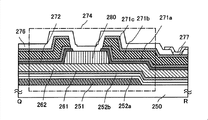
Fig. 1 illustrates the channel cutoff type with bottom-gate structure (the being also referred to as the raceway groove protection type) thin film transistor (TFT) 74 of present embodiment.
In Fig. 1; provide channel cutoff type thin film transistor (TFT) 74 at substrate 50; this channel cutoff type thin film transistor (TFT) 74 comprises gate electrode 51, gate insulating film 52a, gate insulating film 52b, microcrystalline semiconductor film 61, cushion 62, channel protective layer 80, source region and drain region 72, source electrode and drain electrode 71a, source electrode and drain electrode 71b and source electrode and drain electrode 71c, and provides contiguously pixel electrode 77 with source electrode and drain electrode 71c.Mode with the part of cover film transistor 74 and pixel electrode 77 provides dielectric film 76.In addition, Fig. 1 is corresponding to Fig. 4 D.
Owing to having therebetween cushion 62 provides channel protective layer 80 in the channel formation region territory of microcrystalline semiconductor film 61 structure, so can prevent the suffered damage (reduction of the film thickness that the plasma that uses during etching or etchant cause or oxidation etc.) of cushion 62 on the channel formation region territory of microcrystalline semiconductor film 61 in carrying out operation.Thus, can improve the reliability of thin film transistor (TFT) 74.In addition, because the cushion 62 on the channel formation region territory of microcrystalline semiconductor film 61 is not etched, so do not need cushion 62 is formed thick, and can shorten film formation time.
In addition, the end of the gate electrode 51 that the end of microcrystalline semiconductor film 61 is more overlapping than sandwich gate insulating film 52a and 52b more in the inner part, it does not exceed gate electrode 51 scope be formed on the gate electrode 51.Thus, can form microcrystalline semiconductor film 61 by the flat site on gate electrode 51, gate insulating film 52a and gate insulating film 52b, thereby can obtain the film that spreadability is good and have therein uniform properties (crystalline state).
Hereinafter, describe manufacture method in detail.Form gate electrode 51 (with reference to Fig. 2 A and Fig. 4 A) at substrate 50.Fig. 2 A is equivalent to along the sectional view of the line A-B among Fig. 4 A.As substrate 50, can use such as barium borosilicate glass, aluminium borosilicate glass, alumina silicate glass etc. of alkali-free glass substrate of making by fusion method or float glass process; Or ceramic substrate, can also use stable on heating plastic with the treatment temperature that can bear this manufacturing process etc.In addition, can also use the substrate that dielectric film is set on metal substrate surfaces such as stainless steel alloies.The size of substrate 50 can adopt 320mm * 400mm, 370mm * 470mm, 550mm * 650mm, 600mm * 720mm, 680mm * 880mm, 730mm * 920mm, 1000mm * 1200mm, 1100mm * 1250mm, 1150mm * 1300mm, 1500mm * 1800mm, 1900mm * 2200mm, 2160mm * 2460mm, 2400mm * 2800mm or 2850mm * 3050mm etc.
Note, form semiconductor film or wirings at gate electrode 51, so its end is preferably processed to conical by its shape, disconnect in order to prevent.In addition, although not shown, also can form simultaneously the wiring that is connected to gate electrode by the operation that forms gate electrode.
Then, on gate electrode 51, form successively gate insulating film 52a, gate insulating film 52b, microcrystalline semiconductor film 53 and cushion 54 (with reference to Fig. 2 B).
Can when carrying out the hydrogen plasma processing (or carrying out after the hydrogen plasma processing), microcrystalline semiconductor film 53 be formed on the surface of gate insulating film 52b.If form microcrystalline semiconductor film at the gate insulating film that has carried out the hydrogen plasma processing, then can promote the crystal growth of crystallite.In addition, can reduce the distortion of lattice at the interface between gate insulating film and the microcrystalline semiconductor film, and can improve the interfacial characteristics between gate insulating film and the microcrystalline semiconductor film, the electrical characteristics of the microcrystalline semiconductor film that therefore obtains are high and reliability is high.
In addition, also can not be exposed to atmosphere ground and form continuously gate insulating film 52a, gate insulating film 52b, microcrystalline semiconductor film 53 and cushion 54.Form continuously gate insulating film 52a, gate insulating film 52b, microcrystalline semiconductor film 53 and cushion 54 by not being exposed to atmosphere ground, form the interface of each lamination in the situation that the pollution impurity element that can suspend pollutes in not being subject to Atmospheric components or atmosphere, therefore, can reduce the unevenness of tft characteristics.
Example as three layer laminate structures of gate insulating film, can form silicon nitride film or silicon oxynitride film as ground floor at gate electrode, stacked oxygen silicon nitride membrane is as the second layer, and stacked silicon nitride film is as the 3rd layer, and forms microcrystalline semiconductor film at the silicon nitride film of the superiors.In the case, the silicon nitride film of ground floor or the thickness of silicon oxynitride film are preferably greater than 50nm, and this film has the effect as the barrier film of the impurity that stops sodium etc., and has the effect of generation and the gate electrode oxidation of the hillock that prevents gate electrode.The 3rd layer silicon nitride film has the effect of the compactedness that improves microcrystalline semiconductor film and when carrying out microcrystalline semiconductor film is carried out Ear Mucosa Treated by He Ne Laser Irradiation, prevents the effect of oxidation when namely LP processes.
Like this, by form nitride film such as silicon nitride film as thin as a wafer on the gate insulating film surface, can improve the compactedness of microcrystalline semiconductor film.Nitride film can form by plasma CVD method, also can carry out nitrogen treatment by the high density of use microwave and the Cement Composite Treated by Plasma of low temperature.In addition, also can carry out forming silicon nitride film, silicon oxynitride film when the silane flushing is processed to reaction chamber.
At this, oxygen silicon nitride membrane is higher than the film of nitrogen content for oxygen content in forming at it, wherein the concentration range with 55 atom % to 65 atom % comprises oxygen, scope with 1 atom % to 20 atom % comprises nitrogen, scope with 25 atom % to 35 atom % comprises Si, comprises hydrogen with the scope of 0.1 atom % to 10 atom %.In addition, silicon oxynitride film is higher than the film of oxygen content for nitrogen content in forming at it, wherein the concentration range with 15 atom % to 30 atom % comprises oxygen, scope with 20 atom % to 35 atom % comprises nitrogen, scope with 25 atom % to 35 atom % comprises Si, comprises hydrogen with the scope of 15 atom % to 25 atom %.
This microcrystalline semiconductor film can be tens MHz to the high frequency plasma cvd method of hundreds of MHz or frequency by frequency is that microwave plasma CVD device more than the 1GHz forms.Typically say, can use hydrogen dilute Si H
4, Si
2H
6, SiH
2Cl
2, SiHCl
3, SiCl
4, SiF
4Deng silane form microcrystalline semiconductor film.In addition, can add one or more the rare gas element that is selected from helium, argon, krypton, the neon to silane and hydrogen and dilute to form microcrystalline semiconductor film.To be set as with respect to the throughput ratio of hydrogen of the silane of this moment more than 5 times below 200 times, be preferably more than 50 times below 150 times more preferably 100 times.
In addition, because microcrystalline semiconductor film be not to add wittingly to present faint N-shaped electric conductivity when being controlled to be the impurity element of purpose with valence electron, so can be by when carrying out film forming or carrying out film forming after the impurity element of giving p-type as the microcrystalline semiconductor film interpolation in the channel formation region territory of thin film transistor (TFT) being controlled threshold value.As the impurity element of giving p-type, the typical case has boron, preferably with B
2H
6, BF
3Deng foreign gas with 1ppm to 1000ppm, preferably sneak in the silane with the ratio of 1ppm to 100ppm.And, preferably boron concentration for example is set as 1 * 10
14Atoms/cm
3To 6 * 10
16Atoms/cm
3
In addition, the oxygen concentration of microcrystalline semiconductor film is 5 * 10
19Atoms/cm
-3Below, be preferably 1 * 10
19Atoms/cm
-3Below, the concentration of nitrogen and carbon preferably is respectively 1 * 10
18Atoms/cm
-3Below.Be blended into oxygen in the microcrystalline semiconductor film, nitrogen, and the concentration of carbon by reduction, can prevent the N-shaped of microcrystalline semiconductor film.
To be thicker than below the 0nm to 50nm, the thickness that preferably is thicker than below the 0nm to 20nm forms microcrystalline semiconductor film 53.
In addition, the mobility ratio amorphous semiconductor film of microcrystalline semiconductor film is high.Therefore, by using thin film transistor (TFT) that its channel formation region territory forms by microcrystalline semiconductor film as the switch of display element, can dwindle the area in channel formation region territory, i.e. the area of thin film transistor (TFT).Thus, the area reducing that the thin film transistor (TFT) in each pixel is shared, thus can improve the aperture opening ratio of pixel.As a result, can make the high device of resolution.
In addition, microcrystalline semiconductor film is from following acicular crystal with the longitudinal direction growth.Mixing exists noncrystal and crystal structure in microcrystalline semiconductor film, easily produces the crack that causes because of local stress and the gap occurs between crystalline region and amorphous area.Other free radical enters this gap and can cause the crystal growth.Yet, because the increase of top crystal face, so be easy to upwards growth of needle-like.Like this, though microcrystalline semiconductor film grow with longitudinal direction, its speed also be the amorphous semiconductor film film forming speed 1/10 to 1/100.
Can be by using SiH
4, Si
2H
6, SiH
2C1
2, SiHCl
3, SiCl
4, SiF
4Deng silicon gas (silane gas, silicon halide gas) and using plasma CVD method form cushion 54.In addition, can dilute to form amorphous semiconductor film with one or more the rare gas element that is selected from helium, argon, krypton, the neon to above-mentioned silane.By using its flow to be more than 1 times below 20 times of the flow of silane, be preferably more than 1 times below 10 times, more preferably the hydrogen below 5 times more than 1 times can form the amorphous semiconductor film that comprises hydrogen.In addition, by using above-mentioned silane and nitrogen or ammonia, can form the amorphous semiconductor film that comprises nitrogen.In addition, by using above-mentioned silane and the gas (F that comprises fluorine, chlorine, bromine or iodine
2, Cl
2, Br
2, I
2, HF, HCl, HBr, HI etc.), can form the amorphous semiconductor film that comprises fluorine, chlorine, bromine or iodine.
In addition, as cushion 54, can be with amorphous semiconductor as target and carry out sputter with hydrogen or rare gas and form amorphous semiconductor film.At this moment, by with ammonia, nitrogen or N
2O is included in the atmosphere, can form the amorphous semiconductor film that contains nitrogen.In addition, by containing the gas (F of fluorine, chlorine, bromine or iodine
2, Cl
2, Br
2, I
2, HF, HCl, HBr, HI etc.) be included in the atmosphere, can form the amorphous semiconductor film that contains fluorine, chlorine, bromine or iodine.
In addition, as cushion 54, also can be on the surface of microcrystalline semiconductor film 53 using plasma CVD method or sputtering method form amorphous semiconductor film, then the surface of amorphous semiconductor film is used the processing of hydrogen plasma, nitrogen plasma, halogen plasma or rare gas (helium, argon, krypton, neon) plasma, make amorphous semiconductor film surface hydriding, nitrogenize or halogenation.
The preferred amorphous semiconductor film that uses forms cushion 54.Therefore, being tens MHz at proportion forms in the situation of amorphous semiconductor film to high frequency plasma cvd method or the microwave plasma CVD technique of hundreds of MHz, preferably controls membrance casting condition so that it becomes amorphous semiconductor film.
Typically say, cushion 54 preferably forms with the thickness below the above 50nm of 10nm.The total concentration that in addition, preferably will be included in nitrogen, carbon and oxygen in the cushion is set as 1 * 10
20Atoms/cm
3To 15 * 10
20Atoms/cm
3If above-mentioned concentration even then thickness is below the above 50nm of 10nm, also can make cushion 54 as high resistance area.
Also can be below the above 200nm of 150nm with the thickness setting of cushion 54, each concentration of the carbon that comprises, nitrogen, oxygen is set as 3 * 10
19Atoms/cm
3Below, be preferably 5 * 10
18Atoms/cm
3Below.
As cushion, can prevent from being included in the autoxidation on the surface of the crystal grain in the microcrystalline semiconductor film 53 by the amorphous semiconductor film that forms amorphous semiconductor film on the surface of microcrystalline semiconductor film 53 or comprise hydrogen, nitrogen or halogen.Form cushion by the surface at microcrystalline semiconductor film 53, can prevent the oxidation of micrinite.By in cushion, sneaking into hydrogen and/or fluorine, can prevent that block enters in the microcrystalline semiconductor film.
In addition, because the amorphous semiconductor film that uses amorphous semiconductor film or use to comprise hydrogen, nitrogen or halogen forms cushion 54, so the resistance ratio of cushion 54 is high as the resistance of the microcrystalline semiconductor film in channel formation region territory.Thus, in the thin film transistor (TFT) that forms in the back, the cushion that is formed between source region and drain region and the microcrystalline semiconductor film is used as high resistance area.Therefore, can reduce the cut-off current of thin film transistor (TFT).When this thin film transistor (TFT) is used as the on-off element of liquid crystal indicator, can improve the contrast of liquid crystal indicator.
Then, be formed on overlappingly channel protective layer 80 (with reference to Fig. 2 C) on the cushion 54 with the channel formation region territory of microcrystalline semiconductor film 53.Channel protective layer 80 can not be exposed to atmosphere ground with gate insulating film 52a, gate insulating film 52b, microcrystalline semiconductor film 53 and cushion 54 yet and forms continuously.Do not want stacked film if be not exposed to continuous formation the in atmosphere ground, productivity then improves.
As channel protective layer 80, can use inorganic material (monox, silicon nitride, silicon oxynitride, silicon oxynitride etc.).Can use the organic material (organic resin material) (polyimide, acrylic acid, polyamide, polyimide amide, resist, benzocyclobutene etc.) of photosensitive or non-photosensitivity, by the multiple film that consists of of this material or the lamination of these films etc.In addition, also can use siloxane.As manufacture method, can using plasma CVD method, vapor growth method or the sputtering method of hot CVD method etc.In addition, also can adopt coating process, liquid droplet ejection method, print process (method of the formation pattern of serigraphy or lithography etc.) such as spin-coating method etc. as wet method.Channel protective layer 80 both can process to form by etching after film forming, again can be by optionally formation such as liquid droplet ejection method.
Then, by etching microcrystalline semiconductor film 53 and cushion 54 are processed, to form the lamination (with reference to Fig. 2 D) of microcrystalline semiconductor film 61 and cushion 62.Can form mask by photoetching technique or liquid droplet ejection method, and form microcrystalline semiconductor film 61 and cushion 62 with this mask etching microcrystalline semiconductor film 53 and cushion 54.In addition, Fig. 2 D is equivalent to along the sectional view of the A-B of Fig. 4 B.
The end of microcrystalline semiconductor film 61, cushion 62 can be etched into taper.The bevel angle of end is set as 30 degree to 90 degree, is preferably 45 degree to 80 degree.Thus, can prevent the disconnection of the wiring that causes owing to step shape.
Then, form semiconductor film 63 and the conducting film 65a to 65c (with reference to Fig. 3 A) that is added with the impurity of giving a kind of conduction type in gate insulating film 52b, microcrystalline semiconductor film 61, cushion 62, channel protective layer 80.Form mask 66 at the semiconductor film 63 that is added with the impurity of giving a kind of conduction type and conducting film 65a to 65c.Mask 66 forms by photoetching technique or ink-jet method.
In the situation that form n channel-type thin film transistor (TFT), for the semiconductor film 63 that is added with the impurity of giving a kind of conduction type, add phosphorus as the exemplary impurity element and get final product, namely add PH for silane
3Deng foreign gas get final product.In addition, in the situation that form p channel-type thin film transistor (TFT), add boron as the exemplary impurity element and get final product, namely add B for silane
2H
6Deng foreign gas get final product.Can use crystallite semiconductor or amorphous semiconductor to form the semiconductor film 63 that is added with the impurity of giving a kind of conduction type.The semiconductor film 63 that is added with the impurity of giving a kind of conduction type is formed have 2nm to the 50nm thickness of (being preferably 10nm to 30nm).
Preferred use aluminium, copper or be added with the stable on heating element of raisings such as silicon, titanium, neodymium, scandium, molybdenum or prevent individual layer or the lamination formation conducting film of the aluminium alloy of the element that hillock produces.In addition, also can adopt following rhythmo structure: use the nitride formation of titanium, tantalum, molybdenum, tungsten or above-mentioned element to contact the film of a side with the semiconductor film that is added with the impurity of giving a kind of conduction type, and form aluminum or aluminum alloy thereon.Moreover, can also adopt following rhythmo structure: use the nitride of titanium, tantalum, molybdenum, tungsten or above-mentioned element below top the reaching of aluminum or aluminum alloy, to clamp.At this, as conducting film the conducting film with three layers the structure that is laminated with conducting film 65a to 65c is shown, for example illustrate with the molybdenum film as conducting film 65a, 65c and with the aluminium film as the lamination conducting film of conducting film 65b and with titanium film as conducting film 65a, 65c and with the lamination conducting film of aluminium film as conducting film 65b.
Form conducting film 65a to 65c by sputtering method and vacuum vapour deposition.In addition, also can form conducting film 65a to 65c by the ejections such as silk screen print method, ink-jet method and roasting with the electrical-conductive nanometer cream of silver, gold, copper etc.
Then, separate conducting film 65a to 65c with mask 66 etchings, to form source electrode and drain electrode 71a to 71c (with reference to Fig. 3 B).As Fig. 3 B of present embodiment, conducting film 65a to 65c is carried out wet etching, conducting film 65a to 65c is etched in isotropic mode, thereby the end of the end of mask 66 and source electrode and drain electrode 71a to 71c is inconsistent, and the end of source electrode and drain electrode 71a to 71c is in the inside.Then, the semiconductor film 63 that is added with the impurity of giving a kind of conduction type with mask 66 etchings forms source region and drain region 72 (with reference to Fig. 3 C).Note, because channel protective layer 80 is as channel stop layer, so cushion 62 is not etched.
The end in the end of source electrode and drain electrode 71a to 71c and source region and drain region 72 is inconsistent and depart from, and namely forms the end in source region and drain region 72 in the outside of the end of source electrode and drain electrode 71a to 71c.Then, remove mask 66.Note, Fig. 3 C is equivalent to along the sectional view of the line A-B of Fig. 4 C.From Fig. 4 C as can be known, the end in source region and drain region 72 is positioned at the outside of the end of source electrode and drain electrode 71c.In other words, as can be known, the area in source region and drain region 72 is greater than the area of source electrode and drain electrode 71a to 71c.In addition, a side of source electrode or drain electrode also plays the function of source wiring or leak routing.
Shown in Fig. 3 C, owing to inconsistent the departing from of end in end and source region and the drain region 72 of source electrode and drain electrode 71a to 71c, so the distance of the end of source electrode and drain electrode 71a to 71c from, thereby can prevent leakage current and short circuit between source electrode and the drain electrode.In other words, as can be known, source region and drain region exceed the end of source electrode and drain electrode, and the distance between the end in source region respect to one another and drain region is shorter than the distance between the end of source respect to one another electrode and drain electrode.Therefore thin film transistor (TFT) that can fabrication reliability is high and resistance to pressure is high.
By above-mentioned operation, can form channel cutoff (protection) type thin film transistor (TFT) 74.
The cushion 62 that is formed on the cushion 62 under source region and the drain region 72 and is formed on the channel formation region territory of microcrystalline semiconductor film 61 is the continuous films that consisted of and formed simultaneously by same material.Cushion 62 on the microcrystalline semiconductor film 61 utilizes the hydrogen that comprises to prevent entering of extraneous air and etch residue, with protection microcrystalline semiconductor film 61.
Do not mix each other by the impurity of giving a kind of conduction type that the cushion 62 that does not comprise the impurity of giving a kind of conduction type is provided, can makes the impurity of giving a kind of conduction type that is included in source region and drain region and be used for the threshold voltage of control microcrystalline semiconductor film 61.When a kind of impurity of conduction type is given in mixing, produce recombination centers, leakage current flows through, thereby can not obtain to reduce the effect of cut-off current.
By cushion and channel protective layer as above are provided like that, can make the resistance to pressure high channel cutoff type thin film transistor (TFT) that leakage current has reduced.Thus, can also reliability high and suitably be applied to the thin film transistor (TFT) that is used for liquid crystal indicator of the voltage that applies 15V.
Then, form the pixel electrode 77 that contacts with source electrode or drain electrode 71c.Form dielectric film 76 at source electrode and drain electrode 71a to 71c, source region and drain region 72, channel protective layer 80, gate insulating film 52b and pixel electrode 77.Dielectric film 76 can similarly form with gate insulating film 52a and 52b.In addition, dielectric film 76 provides for the entering of pollution impurity that prevents from being suspended in organism, metal object or water vapor etc. in the atmosphere, therefore is preferably fine and close film.
Typically say, cushion 62 preferably forms with the thickness below the above 50nm of 10nm.Cushion 62 on the channel formation region territory of microcrystalline semiconductor film 61 does not have etched, and therefore, cushion 62 needn't form thick, and can shorten film formation time.The total concentration that in addition, preferably will be included in nitrogen, carbon and oxygen in the cushion is set as 1 * 10
20Atoms/cm
3To 15 * 10
20Atoms/cm
3If above-mentioned concentration even then thickness is below the above 50nm of 10nm, also can make cushion 62 as high resistance area.
Yet, also can form cushion 62 with the thickness below the above 200nm of 150nm, and carbon, nitrogen, the oxygen concentration that comprises is set as 3 * 10
19Atoms/cm
3Below, be preferably 5 * 10
18Atoms/cm
3Below.In the case, by silicon nitride film is used as dielectric film 76, the oxygen concentration in the cushion 62 can be set as 5 * 10
19Atoms/cm
3Below, be preferably 1 * 10
19Atoms/cm
3Below.
Then, etching dielectric film 76 exposes the part of pixel electrode 77.Can be to form liquid crystal cell with the mode that contacts of zone of exposing of pixel electrode 77, so that thin film transistor (TFT) 74 and liquid crystal cell are electrically connected to each other.For example, form alignment films at pixel electrode 77, make it and the comparative electrode face-off that alignment films similarly is provided, and the formation liquid crystal layer gets final product between alignment films.
As pixel electrode 77, can use conductive material such as the indium oxide that comprises tungsten oxide with light transmission, the indium-zinc oxide that comprises tungsten oxide, the indium oxide that comprises titanium dioxide, the indium tin oxide that comprises titanium dioxide, indium tin oxide (below be called ITO), indium-zinc oxide, be added with the indium tin oxide of monox etc.
In addition, also can use the conductive composition that comprises conducting polymer (being also referred to as conductive polymer) to form pixel electrode 77.The pixel electrode that uses conductive composition to form preferably has following condition: sheet resistance is 10000 Ω/m
2Below, the transmittance when wavelength is 550nm is more than 70%.In addition, the resistivity that is included in the conducting polymer in the conductive composition is preferably below the 0.1 Ω cm.
As conducting polymer, can use so-called pi-electron conjugate class conducting polymer.For example, can enumerate polyaniline or derivatives thereof, polypyrrole or derivatives thereof, polythiophene or derivatives thereof or by two or more in the above-mentioned substance and interpolymer that consists of etc.
In addition, also can adopt the end shape consistent with the end of source electrode and drain electrode in source region and drain region.Figure 26 illustrates the channel cutoff type thin film transistor (TFT) 79 of end with source region and drain region shape consistent with the end of source electrode and drain electrode.When being undertaken for the etching of source electrode and drain electrode by dry ecthing and during for the etching in source region and drain region, can obtaining the shape as thin film transistor (TFT) 79.In addition, when the semiconductor film that source electrode and drain electrode are added with the impurity of giving a kind of conduction type as mask etching forms source region and drain region, also can obtain the shape as thin film transistor (TFT) 79.
By forming channel cutoff type thin film transistor (TFT), can improve the reliability of thin film transistor (TFT).In addition, form the zone by using the microcrystalline semiconductor film constituting channel, can obtain 1cm
2/ Vsec to 20cm
2The field effect mobility of/Vsec.Therefore, this thin film transistor (TFT) can be used as the on-off element of the pixel of pixel section, but also can be as the element of the driving circuit that forms sweep trace (gate line) side.
By present embodiment, can make the liquid crystal indicator with the high and thin film transistor (TFT) that reliability is high of electrical characteristics.
Embodiment 2
The example that the shape that present embodiment is described thin film transistor (TFT) and embodiment 1 are different.Therefore, other parts can similarly form with embodiment 1, thereby omit for the part identical with embodiment 1, the repeat specification with part and same processes of identical function.
In the present embodiment, use Fig. 5, Fig. 6 A to 6D and Figure 27 explanation to be used for thin film transistor (TFT) and the manufacturing process thereof of liquid crystal indicator.Fig. 5 and Figure 27 are the sectional view that thin film transistor (TFT) and pixel electrode are shown, and Fig. 6 A to 6D is the vertical view of the join domain of thin film transistor (TFT) in a pixel and pixel electrode.Fig. 5 and Figure 27 are equivalent to along the thin film transistor (TFT) of the line Q-R among Fig. 6 A to 6D and the sectional view of manufacturing process thereof.
Channel cutoff type (the being also referred to as the raceway groove protection type) thin film transistor (TFT) 274 of the bottom grating structure of present embodiment is illustrated in Fig. 5 and Fig. 6 A to 6D.
In Fig. 5; provide channel cutoff type thin film transistor (TFT) 274 at substrate 250; this channel cutoff type thin film transistor (TFT) 274 comprises gate electrode 251, gate insulating film 252a, gate insulating film 252b, microcrystalline semiconductor film 261, cushion 262, channel protective layer 280, source region and drain region 272, source electrode and drain electrode 271a, source electrode and drain electrode 271b and source electrode and drain electrode 271c, and provides dielectric film 276 in the mode of cover film transistor 274.Provide contiguously pixel electrode 277 with source electrode and drain electrode 271c in the contact hole in being formed on dielectric film 276.Note, Fig. 5 is corresponding to Fig. 6 D.
Owing to having sandwich cushion 262 provides channel protective layer 280 in the channel formation region territory of microcrystalline semiconductor film 261 structure, so can prevent the suffered damage (reduction of the film thickness that the free radical of the plasma that uses during etching or etchant cause or oxidation etc.) when carrying out operation of cushion 262 on the channel formation region territory of microcrystalline semiconductor film 261.Thus, can improve the reliability of thin film transistor (TFT) 274.In addition, because the cushion 262 on the channel formation region territory of microcrystalline semiconductor film 261 is not etched, so do not need cushion 262 is formed thick, and can shorten film formation time.
Hereinafter, use Fig. 6 A to 6D that manufacture method is described.Form gate electrode 251 (with reference to Fig. 6 A) at substrate 250.Form gate insulating film 252a, gate insulating film 252b, microcrystalline semiconductor film and cushion 262 at gate electrode 251.Be formed on overlappingly channel protective layer 280 (with reference to Fig. 6 A) on the cushion 262 with the channel formation region territory of microcrystalline semiconductor film.
Although in embodiment 1, illustrated after forming channel protective layer 80 and microcrystalline semiconductor film 53 and cushion 54 to have been carried out etching work procedure they are processed into the example of island microcrystalline semiconductor film 61 and cushion 62, illustrated in the present embodiment by with etching source electrode and drain electrode and be added with the identical operation of the semiconductor film of the impurity of giving a kind of conduction type and carry out example for the etching work procedure of microcrystalline semiconductor film and cushion.Thus, use identical mask to form microcrystalline semiconductor film, cushion, the semiconductor film that is added with the impurity of giving a kind of conduction type, source electrode and drain electrode.Like this, carry out simultaneously etching work procedure, the number of not only simplifying working process, and can reduce number of masks for etching work procedure.
By etching microcrystalline semiconductor film, cushion, the semiconductor film that is added with the impurity of giving a kind of conduction type and conducting film, form microcrystalline semiconductor film 261, cushion 262, source region and drain region 272 and source electrode and drain electrode 271a to 271c, to form channel cutoff type thin film transistor (TFT) 274 (with reference to Fig. 6 C).Form the dielectric film 276 on the cover film transistor 274, and form the contact hole of arrival source electrode and drain electrode 271c.In contact hole, form pixel electrode 277 with thin film transistor (TFT) 274 and pixel electrode 277 be electrically connected to each other (with reference to Fig. 6 D).
In addition, also can adopt the end shape consistent with the end of source electrode and drain electrode in source region and drain region.Figure 27 illustrates the channel cutoff type thin film transistor (TFT) 279 of end with source region and drain region shape consistent with the end of source electrode and drain electrode.When being undertaken for the etching of source electrode and drain electrode by dry ecthing and during for the etching in source region and drain region, can obtaining the shape as thin film transistor (TFT) 279.In addition, when the semiconductor film that source electrode and drain electrode are added with the impurity of giving a kind of conduction type as mask etching forms source region and drain region, also can obtain the shape as thin film transistor (TFT) 279.
By forming the thin film transistor (TFT) of channel cutoff type, can improve the reliability of thin film transistor (TFT).In addition, form the zone by using the microcrystalline semiconductor film constituting channel, can obtain 1cm
2/ Vsec to 20cm
2The field effect mobility of/Vsec.Therefore, this thin film transistor (TFT) can be used as the on-off element of the pixel of pixel section, but also can be as the element of the driving circuit that forms sweep trace (gate line) side.
By present embodiment, can make the liquid crystal indicator with the high and thin film transistor (TFT) that reliability is high of electrical characteristics.
Embodiment 3
In the present embodiment, with the example of explanation to the manufacturing process of microcrystalline semiconductor film irradiating laser.
Form gate electrode at substrate, and form gate insulating film in the mode of covering grid electrode.Then on gate insulating film stacked microcrystal silicon (SAS) film as microcrystalline semiconductor film.The thickness 1nm of microcrystalline semiconductor film is above less than 15nm, more preferably below the above 10nm of 2nm.Especially having 5nm (4nm to 8nm) when thick, high for the absorptivity of laser, and improve productivity.
In the situation that by plasma CVD method etc. microcrystalline semiconductor film is formed on the gate insulating film, the near interface at gate insulating film and the crystalliferous semiconductor film of bag forms the zone (referred to herein as interface zone) that comprises the amorphous component of Duoing than semiconductor film sometimes.In addition, in the situation that by formation thickness such as plasma CVD methods is the as thin as a wafer microcrystalline semiconductor film below about 10nm, although can form the semiconductor film that comprises microcrystal grain, be not easy to obtain in whole film, to comprise equably the semiconductor film of the measured microcrystal grain of matter.The laser treatment of irradiating laser in the case, shown below is effective.
Next, from the surface one side irradiating laser of microcrystalline sillicon film.With the infusible energy density irradiating laser of microcrystalline sillicon film.In other words, the laser treatment of present embodiment (Laser Process below is also referred to as " LP ") utilizes the solid phase crystal to grow to carry out, and does not wherein make microcrystalline sillicon film raying heating and melts.In other words, this laser treatment is to utilize half stacked crystal silicon film not become the critical zone of liquid phase, therefore, also can be called " critical growth ".
Can make laser action arrive the interface of microcrystalline sillicon film and gate insulating film.Thus, can with at the crystal of the surface of microcrystalline sillicon film one side as seed, the interface of crystal from this surface to gate insulating film carried out the growth of solid phase crystal and the roughly crystal of column occurred.The solid phase crystal growth of processing by LP is not to enlarge particle diameter, but improves the crystallinity on film thickness direction.
In LP processes, be long rectangular-shaped (linear laser) by laser is gathered, can carry out a laser scanning and process microcrystalline sillicon film on the glass substrate of 730mm * 920mm for example.In the case, the ratio of overlapping linear laser (Duplication) is 0% to 90% (being preferably 0% to 67%).Thus, the reduction of the processing time of each substrate, and can boost productivity.The shape of laser is not limited to wire, can use planar laser similarly to process.In addition, this LP processes the size that is not limited to above-mentioned glass substrate, can be suitable for various sizes.
Process by LP, improve the crystallinity of gate insulating film interface zone, and have the effect of the electrical characteristics that improve the thin film transistor (TFT) with bottom-gate structure as the thin film transistor (TFT) of present embodiment.
One of feature of this critical growth is as follows, namely is not formed on the concave-convex surface (being also referred to as the convex body of ridge (ridge)) that exists in the conventional low temperature polycrystalline silicon, and the silicon face after LP processes keeps flatness.
Shown in present embodiment, the crystal silicon film that the microcrystalline sillicon film direct irradiation laser after the film forming is obtained and conventional only stacking microcrystalline sillicon film and the microcrystalline sillicon film (being recorded in the above-mentioned non-patent literature 1) by conduction heating change character are showing different in nature at growth mechanism and film.In this manual, will carry out that LP processes and the crystalline semiconductor film that has that obtains is called the LPSAS film to the microcrystalline semiconductor film after the film forming.
After forming the microcrystalline semiconductor film of LPSAS film etc., form amorphous silicon (a-Si:H) film as cushion by plasma CVD method with 300 ℃ to 400 ℃ temperature.Process by this film forming, hydrogen is fed into the LPSAS film, and can obtain the effect identical with making the hydrogenation of LPSAS film.In other words, by stacked amorphous silicon film on the LPSAS film, can be in the LPSAS film diffusible hydrogen, dangling bonds terminates.
Following operation is identical with embodiment 1, wherein forms channel protective layer, and forms mask thereon.Then, separate microcrystalline semiconductor film and cushion with mask etching.Next, form the semiconductor film that is added with the impurity of giving a kind of conduction type, form conducting film, and form mask at its conducting film.Then, separate conducting film with this mask etching, to form source electrode and drain electrode.Moreover, with identical mask channel protective layer is come etching as etching stopping layer, to form source region and drain region.
By above-mentioned operation, can form the thin film transistor (TFT) of channel cutoff type, and can make the liquid crystal indicator that comprises channel cutoff type thin film transistor (TFT).
In addition, present embodiment can freely make up with embodiment 1 or embodiment 2.
Embodiment 4
In the present embodiment, describe the example of the manufacturing process of the liquid crystal indicator in the embodiment 1 to 3 in detail.Therefore, omit for the part identical with embodiment 1 to 3 or explanation with part and identical operation of identical function.
In embodiment 1 to 3, can also be before forming microcrystalline semiconductor film reaction chamber be carried out cleaning treatment and (use hydrogen as the hydrogen flushing of irrigation, use silane as the silane flushing of irrigation etc.) processed in flushing (washing).Process by flushing, can prevent the pollution that the impurity of oxygen, nitrogen, fluorine etc. in the reaction chamber brings to the film that will form.
Process by means of flushing, can remove the impurity of oxygen in the reaction chamber, nitrogen, fluorine etc.For example, by using plasma CVD equipment to use monosilane as irrigation, under the condition of the gas flow of 8SLM to 10SLM and 5 minutes to 20 minutes (being preferably 10 minutes to 15 minutes), monosilane is incorporated in the reaction chamber continuously, processes to carry out the silane flushing.Note, 1SLM is equivalent to 1000sccm, namely is 0.06m
3/ h.
For example can utilize fluorine-based the cleaning.Note, by fluorocarbons, nitrogen fluoride or fluorine being incorporated in the plasma generator that is arranged on the reaction chamber outside and from solution, then be incorporated in the reaction chamber fluorine-based, can clean reaction chamber.
Also can before forming gate insulating film, cushion, channel protective layer and being added with the semiconductor film of the impurity of giving a kind of conduction type, wash processing.Note, it is effective washing processing after cleaning treatment.
Before substrate being moved into reaction chamber and being carried out film forming, also can use by with the processing (being also referred to as precoating processes) of film formed diaphragm coating on the interior wall of each reaction chamber of the film identical type that will form.It is a kind of like this processing that precoating is processed, and namely by film forming gas being flow in the reaction chamber and carrying out Cement Composite Treated by Plasma, utilizes in advance the diaphragm of thin thickness to cover in the reaction chamber.For example, before the formation microcrystalline sillicon film is as microcrystalline semiconductor film, carry out getting final product with the precoating processing in the amorphous silicon film covering reaction chamber of 0.2 μ m to 0.4 μ m.Also can after processing, precoating wash processing (hydrogen flushing, silane flushing etc.).In the situation that carry out cleaning treatment and precoating processing, need to from reaction chamber, take out of substrate, and in the situation that wash processing (hydrogen flushing, silane flushing etc.), can process moving under the state of substrate owing to not carrying out Cement Composite Treated by Plasma.
If in being used to form the reaction chamber of microcrystalline sillicon film, form by the film formed diaphragm of amorphous silicon in advance, and before forming film, carry out hydrogen plasma and process, then diaphragm etched and on substrate the few silicon of deposit, it becomes the nuclear of crystal growth.
Process by means of precoating, can prevent the pollution that the impurity of oxygen, nitrogen, fluorine etc. in the reaction chamber brings to the film that will form.
Also can carry out precoating before forming gate insulating film, being added with the semiconductor film of the impurity of giving a kind of conduction type processes.
Moreover detailed description forms the example of the method for gate insulating film, microcrystalline semiconductor film and cushion.
Use Figure 10 A and 10B explanation to can be used for the example of plasma CVD equipment of the present invention.Figure 10 A and 10B are the microwave plasma CVD devices that can form continuously film.Figure 10 A and 10B are the schematic diagram that the top cross-sectional view of microwave plasma CVD device is shown, and it is for possessing load chamber 1110, relief chamber 1115, reaction chamber (1) 1111 to the structure of reaction chamber (4) 1114 around common chamber 1120.Between common chamber 1120 and each chamber, possess gate valve 1122 to 1127, interfere with each other in each indoor processing of carrying out preventing.Note, reaction chamber is not limited to four, also can have still less or more.If a plurality of reaction chambers are arranged, then can use respectively reaction chamber by each film kind, and can reduce the number of times of cleaning reaction chamber.Figure 10 A is the example with four reaction chambers, and Figure 10 B is the example with three reaction chambers.
Use the plasma CVD equipment of Figure 10 A and 10B to form the example of gate insulating film, microcrystalline semiconductor film, cushion and channel protective layer explanation.Substrate is loaded in the box 1128,1129 of load chamber 1110, relief chamber 1115, and is sent to reaction chamber (1) 1111 to reaction chamber (4) 1114 by the delivery unit 1121 of common chamber 1120.This device can distribute reaction chamber by each accumulating film kind, thereby can under the state of atmosphere contact not form continuously a plurality of different films.In addition, in reaction chamber, both film formation process can be carried out, etching work procedure or Ear Mucosa Treated by He Ne Laser Irradiation operation can be carried out again.If the reaction chamber that carries out various operations is provided, then can under the state of atmosphere contact not carry out a plurality of different operations.
To reaction chamber (4), distinguish stacked formation gate insulating film, microcrystalline semiconductor film, cushion and channel protective layer at each reaction chamber (1).In the case, by changing unstrpped gas, continuously stacked a plurality of different types of film.At this, form gate insulating film, then the silane with silane etc. is incorporated in the reaction chamber, makes the reaction of residual oxygen and silane, and reactant is discharged to the outside of reaction chamber, thereby can reduce residual oxygen concentration in the reaction chamber.As a result, can reduce the oxygen concentration that is included in the microcrystalline semiconductor film.In addition, can prevent from being included in the oxidation of the crystal grain in the microcrystalline semiconductor film.
In addition, in plasma CVD equipment, also identical film can be formed in a plurality of reaction chambers, in order to boost productivity.If can in a plurality of reaction chambers, form identical film, then can form film at a plurality of substrates simultaneously.For example in Figure 10 A; reaction chamber (1) and reaction chamber (2) are used as the reaction chamber that forms microcrystalline semiconductor film; with the reaction chamber of reaction chamber (3) as the formation amorphous semiconductor film, and with the reaction chamber of reaction chamber (4) as the formation channel protective layer.Like this, when at the same time a plurality of substrates being processed, by the reaction chamber of the slow-footed film of a plurality of formation film forming is provided, can boost productivity.
Before substrate being moved into reaction chamber and being carried out film forming, preferably use by with the processing (being also referred to as precoating processes) of film formed diaphragm coating on the interior wall of each reaction chamber of the film identical type that will form.It is a kind of like this processing that precoating is processed, and namely by film forming gas being flow in the reaction chamber and carrying out Cement Composite Treated by Plasma, utilizes in advance the diaphragm of thin thickness to cover in the reaction chamber.For example, before the formation microcrystalline sillicon film is as microcrystalline semiconductor film, carry out getting final product with the precoating processing in the amorphous silicon film covering reaction chamber of 0.2 μ m to 0.4 μ m.Also can after processing, precoating wash processing (hydrogen flushing, silane flushing etc.).In the situation that carry out cleaning treatment and precoating processing, need to from reaction chamber, take out of substrate, and in the situation that wash processing (hydrogen flushing, silane flushing etc.), can process moving under the state of substrate owing to not carrying out Cement Composite Treated by Plasma.
If in being used to form the reaction chamber of microcrystalline sillicon film, form by the film formed diaphragm of amorphous silicon in advance, and before forming film, carry out hydrogen plasma and process, then diaphragm etched and on substrate the few silicon of deposit, it becomes the nuclear of crystal growth.
Like this; because therefore the semiconductor film that can use the microwave plasma CVD device that is connected with a plurality of process chambers to form simultaneously gate insulating film, microcrystalline semiconductor film, cushion, channel protective layer and be added with the impurity of giving a kind of conduction type can improve production.In addition, even in certain reaction chamber, safeguard and clean, also can in other reaction chambers, form film, thereby can improve the pitch time (takt time) of film forming.In addition, because can be not by Atmospheric components and be suspended under the state that the pollution impurity element in the atmosphere pollutes and form each lamination interface, so can reduce characteristic inhomogeneous of thin film transistor (TFT).
Because when using the microwave plasma CVD device of this structure, can in each reaction chamber, form film or a kind of film of similar kind, and under the state that is not exposed to atmosphere, form continuously above-mentioned film, therefore can be not by the residue of established film and be suspended under the state that the impurity element in the atmosphere pollutes and form each lamination interface.
Moreover; also can provide the high frequency generator with microwave generator; the semiconductor film that forms gate insulating film, microcrystalline semiconductor film, channel protective layer and be added with the impurity of giving a kind of conduction type by microwave plasma CVD technique, and form cushion by the high frequency plasma cvd method.
Note, although in the microwave plasma CVD device shown in Figure 10 A and the 10B, be respectively arranged with load chamber and the chamber of removing stage makeup and costume, also can arrange one and load/remove stage makeup and costume the chamber.In addition, in the microwave plasma CVD device, also spare room can be set.Owing to can shorten the heating in each reaction chamber until therefore can boost productivity the heat time heating time of film forming by in spare room, substrate being carried out preheating.In this film forming is processed, select to get final product from the gas of gas supply part supply according to its purpose
The incompatible enforcement of structural group that present embodiment can be suitably put down in writing with other embodiments.
In the present embodiment, use Figure 12 to Figure 25 explanation to have the example of the liquid crystal indicator of the thin film transistor (TFT) shown in the embodiment 1 to 4.The TFT628,629 that is used for the liquid crystal indicator of Figure 12 to Figure 25 can make equally with the thin film transistor (TFT) shown in embodiment 1 or the embodiment 2, and it is the high thin film transistor (TFT) of electrical characteristics and reliability.TFT628 has channel protective layer 608, and TFT629 has channel protective layer 611, and they are as the wrong thin film transistor (TFT) of the reciprocal cross in channel formation region territory with microcrystalline semiconductor film.
At first, VA (vertical orientation) type liquid crystal indicator is shown.VA type liquid crystal indicator is mode a kind of of arrangement of the liquid crystal molecule of control liquid crystal panel.VA type liquid crystal indicator be when not being applied in voltage liquid crystal molecule towards the mode for the vertical direction of panel surface.In the present embodiment, especially managing pixel segmentation is several zones (sub-pixs), makes molecule swing to different directions.Said method is called multidomain (multi-domain) change or multidomain design.In the following description, the liquid crystal indicator that adopts the multidomain design is described.
Figure 13 and Figure 14 illustrate respectively pixel electrode and comparative electrode.Note, Figure 13 is the vertical view that is formed with substrate one side of pixel electrode, and Figure 12 illustrates corresponding to the cross section structure along the G-H line among Figure 13.In addition, Figure 14 is the vertical view that is formed with substrate one side of comparative electrode.In the following description, describe with reference to above-mentioned accompanying drawing.
The substrate 600 that Figure 12 illustrates the stacked TFT628 of being formed with, connected pixel electrode 624 and keeps capacitance part 630 and the relative substrate 601 that is formed with comparative electrode 640 etc. also are injected with the state of liquid crystal.
The position of the formation spacer 642 in relative substrate 601 is formed with photomask 632, the first coloring film 634, the second coloring film 636, the 3rd coloring film 638, comparative electrode 640.By this structure, make to control the height of the projection 644 of orientation of liquid crystal and spacer 642 for different.Form alignment films 648 at pixel electrode 624, on comparative electrode 640, form similarly alignment films 646.Be formed with liquid crystal layer 650 therebetween.
At this, use column spacer that spacer 642 is shown, but also can scatter the pearl spacer.Moreover, also can form spacer 642 at the pixel electrode 624 that is formed on the substrate 600.
Form TFT628, connected pixel electrode 624 and keep capacitance part 630 at substrate 600.Pixel electrode 624 is connected to wiring 618 in contact hole 623, this contact hole 623 connects the dielectric film 620 that covers TFT628, wiring and maintenance capacitance part 630 and the 3rd dielectric film 622 that covers dielectric film 620.Suitably use the thin film transistor (TFT) shown in the embodiment 1 as TFT628.In addition, keep capacitance part 630 to be consisted of by the first capacitance wiring 604, gate insulating film 606 and the second capacitance wiring 617, this first capacitance wiring 604 similarly forms with the grid wiring 602 of TFT628, and this second capacitance wiring 617 similarly forms with wiring 616,618.In addition, in Figure 12 to Figure 15, about TFT628, microcrystalline semiconductor film, cushion, as being added with of source region or drain region give a kind of impurity of conduction type semiconductor film, be also used as source electrode or drain electrode wiring processed by identical operation, and stacked be roughly the same shape.
By overlaid pixel electrode 624, liquid crystal layer 650 and comparative electrode 640, form liquid crystal cell.
Figure 13 illustrates the structure on the substrate 600.Use the material shown in the embodiment 1 to form pixel electrode 624.The line of rabbet joint 625 is set in pixel electrode 624.The line of rabbet joint 625 is used for controlling the orientation of liquid crystal.
TFT629 shown in Figure 13 and connected pixel electrode 626 and maintenance capacitance part 631 can and keep capacitance part 630 similarly form with pixel electrode 624 respectively.TFT628 with TFT629 and 616 is connected with wiring.The pixel of its display panels is made of pixel electrode 624 and pixel electrode 626.Pixel electrode 624 and pixel electrode 626 are sub-pixs.
Figure 14 illustrates the structure of relative substrate one side.Be formed with comparative electrode 640 at photomask 632.Comparative electrode 640 is preferred to be used with the same material of pixel electrode 624 and forms.Be formed with the projection 644 of the orientation of control liquid crystal at comparative electrode 640.In addition, the position according to photomask 632 is formed with spacer 642.
Figure 15 illustrates the equivalent electrical circuit of this dot structure.TFT628 and TFT629 are connected to grid wiring 602, wiring 616.In the case, be different by the current potential that makes capacitance wiring 604 and capacitance wiring 605, it is different can making the work of liquid crystal cell 651 and the work of liquid crystal cell 652.In other words, by the current potential of the wiring 604 of difference control capacitance and capacitance wiring 605, the orientation of critically controlling liquid crystal enlarges the visual angle.
When the pixel electrode 624 that is provided with the line of rabbet joint 625 is applied voltage, near the line of rabbet joint 625, produce electric field strain (tilting electric field).Be configured to mutual interlock by the projection 644 with this line of rabbet joint 625 and relative substrate 601 1 sides, effectively produce tilting electric field and control the orientation of liquid crystal.Thus, in each part, make the direction of liquid crystal aligning for different.In other words, carry out the visual angle that multidomain enlarges liquid crystal panel.
Then, for from above-mentioned different VA type liquid crystal indicator, describe with reference to Figure 16 to Figure 19.
Figure 16 and Figure 17 illustrate the dot structure of VA type liquid crystal panel.Figure 17 is the vertical view of substrate 600, and Figure 16 illustrates corresponding to the cross section structure along transversal Y-Z shown in Figure 17.In the following description, describe with reference to above-mentioned two accompanying drawings.
In its dot structure, a pixel comprises a plurality of pixel electrodes, and each pixel electrode is connected with TFT.Each TFT constitutes by different signals and drives.In other words, in the pixel of multidomain design, has the structure that independently control is applied to the signal of each pixel electrode.
Be formed with photomask 632, the second coloring film 636, comparative electrode 640 at relative substrate 601.In addition, between the second coloring film 636 and comparative electrode 640, form planarization film 637, to prevent the orientational disorder of liquid crystal.Figure 18 illustrates the structure of relative substrate one side.Comparative electrode 640 is common electrodes that use between the different pixel, wherein is formed with the line of rabbet joint 641.Be configured to engagedly by the line of rabbet joint 625 with this line of rabbet joint 641 and pixel electrode 624 and pixel electrode 626 1 sides, can effectively produce tilting electric field and control the orientation of liquid crystal.Thus, can in each part, make the direction of liquid crystal aligning for different, to enlarge the visual angle.
By overlaid pixel electrode 624, liquid crystal layer 650 and comparative electrode 640, form the first liquid crystal cell.In addition, by overlaid pixel electrode 626, liquid crystal layer 650 and comparative electrode 640, form the second liquid crystal cell.In addition, adopt the multidomain structure that is provided with the first liquid crystal cell and the second liquid crystal cell in the pixel.
The liquid crystal indicator of horizontal component of electric field mode then, is shown.The horizontal component of electric field mode is to carry out the mode that gray level is expressed by apply in the horizontal direction the electric field driven liquid crystal for the liquid crystal molecule in the unit.By this mode, the visual angle can be expanded as about 180 degree.In the following description, the liquid crystal indicator that adopts the horizontal component of electric field mode is described.
Figure 20 illustrates the substrate 600 that overlaps to form TFT628 and connected pixel electrode 624 and relative substrate 601 and is injected with the state of liquid crystal.Substrate 601 is formed with photomask 632, the second coloring film 636, planarization film 637 etc. relatively.Pixel electrode is positioned at substrate 600 1 sides, and is not arranged on relative substrate 601 1 sides.Between substrate 600 and relative substrate 601, be formed with liquid crystal layer 650.
Form the first pixel electrode 607, the capacitance wiring 604 that is connected to the first pixel electrode 607 and the TFT628 shown in the embodiment 1 at substrate 600.The first pixel electrode 607 can use the material identical with the pixel electrode 77 shown in the embodiment 1.In addition, the first pixel electrode 607 forms with the shape of roughly dividing into primitive shape.Note, form gate insulating film 606 at the first pixel electrode 607 and capacitance wiring 604.
The wiring 616 of TFT628, wiring 618 are formed on the gate insulating film 606.Wiring 616 is the data lines that transmit vision signal in liquid crystal panel, and is the wiring of extending in one direction, and simultaneously, also being formed by connecting with the source region of TFT628 is side's electrode in source electrode and the drain electrode.Wiring 618 is to become the opposing party's electrode in source electrode and the drain electrode and the wiring that is connected with the second pixel electrode 624.
Form the second dielectric film 620 in wiring 616, wiring 618.In addition, form the second pixel electrode 624 at dielectric film 620, be connected with wiring 618 in the contact hole of this second pixel electrode 624 in being formed on dielectric film 620.Pixel electrode 77 same materials shown in pixel electrode 624 uses and the embodiment 1 form.
By said method, form TFT628 and connected the first pixel electrode 624 at substrate 600.Note, keep electric capacity to be formed between the first pixel electrode 607 and the second pixel electrode 624.
Figure 21 is the vertical view that the structure of pixel electrode is shown.Figure 20 illustrates corresponding to the cross section structure along transversal O-P shown in Figure 21.In pixel electrode 624, the line of rabbet joint 625 is set.The line of rabbet joint 625 is used for controlling the orientation of liquid crystal.In the case, between the first pixel electrode 607 and the second pixel electrode 624, produce electric field.Be formed with gate insulating film 606 between the first pixel electrode 607 and the second pixel electrode 624, but the thickness of gate insulating film 606 is 50nm to 200nm, to be that the liquid crystal layer of 2 μ to 10 μ m is compared fully thin with thickness, therefore in fact at direction (horizontal direction) the generation electric field parallel with substrate 600.Orientation by this electric field controls liquid crystal.By utilizing this electric field that is roughly parallel to the direction of substrate that liquid crystal molecule is rotated in the horizontal direction.In the case because liquid crystal molecule all is in horizontality under any state, so because of the impact of the contrast of viewing angle etc. seldom, thereby enlarge the visual angle.In addition, because the first pixel electrode 607 and the second pixel electrode 624 all are euphotic electrodes, so can improve aperture opening ratio.
Other examples of the liquid crystal indicator of horizontal component of electric field mode then, are described.
Figure 22 and Figure 23 illustrate the dot structure of IPS type liquid crystal indicator.Figure 23 is vertical view, and Figure 22 illustrates corresponding to the cross section structure along transversal I-J shown in Figure 23.In the following description, describe with reference to above-mentioned two accompanying drawings.
Figure 22 illustrates the substrate 600 that overlaps to form TFT628 and connected pixel electrode 624 and relative substrate 601 and is injected with the state of liquid crystal.Substrate 601 is formed with photomask 632, the second coloring film 636, planarization film 637 etc. relatively.Pixel electrode is positioned at substrate 600 1 sides, and is not arranged on relative substrate 601 1 sides.Between substrate 600 and relative substrate 601, be formed with liquid crystal layer 650.
Form the TFT628 shown in common electric potential line 609 and the embodiment 1 at substrate 600.Common electric potential line 609 can form simultaneously with the grid wiring 602 of thin film transistor (TFT) 628.In addition, the first pixel electrode 607 forms with the shape of roughly dividing into primitive shape.
The wiring 616 of TFT628, wiring 618 are formed on the gate insulating film 606.Wiring 616 is the data lines that transmit vision signal in liquid crystal panel, and is the wiring of extending in one direction, and simultaneously, also being formed by connecting with the source region of TFT628 is side's electrode in source electrode and the drain electrode.Wiring 618 is to become the opposing party's electrode in source electrode and the drain electrode and the wiring that is connected with the second pixel electrode 624.
Form the second dielectric film 620 in wiring 616, wiring 618.In addition, form the second pixel electrode 624 at dielectric film 620, be connected with wiring 618 in the contact hole 623 of this second pixel electrode 624 in being formed on dielectric film 620.Pixel electrode 77 same materials shown in pixel electrode 624 uses and the embodiment 1 form.Note, as shown in figure 23, pixel electrode 624 be formed and and the comb poles that forms simultaneously of common electric potential line 609 between produce horizontal component of electric field.The comb teeth part of pixel electrode 624 and the comb poles that forms simultaneously with common electric potential line 609 are engaged.
When producing electric field between the current potential of the current potential that is applied to pixel electrode 624 and common electric potential line 609, by the orientation of this electric field controls liquid crystal.By utilizing this electric field that is roughly parallel to the direction of substrate that liquid crystal molecule is rotated in the horizontal direction.In the case because liquid crystal molecule all is in horizontality under any state, so because of the impact of the contrast of viewing angle etc. seldom, thereby enlarge the visual angle.
Like this, form TFT628 and connected pixel electrode 624 at substrate 600.Keep electric capacity to form by between common electric potential line 609 and capacitance electrode 615, gate insulating film 606 being set.Capacitance electrode 615 and pixel electrode 624 interconnect by contact hole 633.
The mode of the liquid crystal indicator of TN type then, is shown.
Figure 24 and Figure 25 illustrate the dot structure of TN type liquid crystal indicator.Figure 25 is vertical view, and Figure 24 illustrates corresponding to the cross section structure along transversal K-L shown in Figure 25.In the following description, describe with reference to above-mentioned two accompanying drawings.
Be formed with photomask 632, the second coloring film 636, comparative electrode 640 at relative substrate 601.In addition, between the second coloring film 636 and comparative electrode 640, form planarization film 637, to prevent the orientational disorder of liquid crystal.Liquid crystal layer 650 therebetween alignment films 648 and alignment films 646 are formed between pixel electrode 624 and the comparative electrode 640.
By overlaid pixel electrode 624, liquid crystal layer 650 and comparative electrode 640, form liquid crystal cell.
In addition, on substrate 600 or relative substrate 601, also can be formed with color filter, be used for preventing the screened film (black matrix) of disclination (disclination) etc.In addition, the face opposite at the face with being formed with thin film transistor (TFT) of substrate 600 attaches polaroid, and perhaps the opposite face of the face with being formed with comparative electrode 640 at relative substrate 601 attaches polaroid.
By above-mentioned operation, can make liquid crystal indicator.Because the liquid crystal indicator of present embodiment use cut-off current is few and electrical characteristics and the high thin film transistor (TFT) of reliability, therefore becomes the liquid crystal indicator that contrast is high and visibility is high.
Embodiment 6
Then, the below illustrates the structure of display panels (being also referred to as liquid crystal panel) of a mode of liquid crystal indicator of the present invention.
Fig. 9 A illustrates a kind of mode of display panels, wherein only has signal-line driving circuit 6013 to form separately and this signal-line driving circuit 6013 is connected with pixel section 6012 on being formed on substrate 6011.Pixel section 6012 and scan line drive circuit 6014 adopt the thin film transistor (TFT) that uses microcrystalline semiconductor film to form.By adopting the transistor that can obtain the mobility higher than the thin film transistor (TFT) that uses microcrystalline semiconductor film to form signal-line driving circuit, can make the working stability of the signal-line driving circuit that is required the driving frequency higher than scan line drive circuit.Note, signal-line driving circuit 6013 also can be transistor, the thin film transistor (TFT) that uses poly semiconductor that uses single crystal semiconductor or the thin film transistor (TFT) that uses SOI.Pass through respectively FPC6015 supply power current potential, various signals etc. for pixel section 6012, signal-line driving circuit 6013, scan line drive circuit 6014.
In addition, signal-line driving circuit and scan line drive circuit also can be formed on the substrate identical with pixel section together.
In addition, in the situation that form separately driving circuit, the substrate that not necessarily needs to be formed with driving circuit is attached on the substrate that is formed with pixel section, for example also can be attached on the FPC.Fig. 9 B illustrates a kind of mode of display panels, wherein only has signal-line driving circuit 6023 to form separately, and this signal-line driving circuit 6023 is connected with pixel section 6022 and scan line drive circuit 6024 on being formed on substrate 6021.Pixel section 6022 and scan line drive circuit 6024 adopt the thin film transistor (TFT) that uses microcrystalline semiconductor film to form.Signal-line driving circuit 6023 is connected with pixel section 6022 by FPC6025.Pass through respectively FPC6025 supply power current potential, various signals etc. for pixel section 6022, signal-line driving circuit 6023, scan line drive circuit 6024.
In addition, also can adopt the thin film transistor (TFT) that uses microcrystalline semiconductor film only the part of signal-line driving circuit or the part of scan line drive circuit to be formed on the substrate identical with pixel section, and form separately other parts and make it be electrically connected to pixel section.Fig. 9 C illustrates a kind of mode of display panels, the analog switch 6033a that signal-line driving circuit is had is formed on the substrate 6031 identical with pixel section 6032, scan line drive circuit 6034, and is formed on separately the shift register 6033b that signal-line driving circuit has on the different substrates and fits each other.Pixel section 6032 and scan line drive circuit 6034 adopt the thin film transistor (TFT) that uses microcrystalline semiconductor film to form.The shift register 6033b that signal-line driving circuit has is connected with pixel section 6032 by FPC6035.Pass through respectively FPC6035 supply power current potential, various signals etc. for pixel section 6032, signal-line driving circuit, scan line drive circuit 6034.
Shown in Fig. 9 A to 9C, in liquid crystal indicator of the present invention, can adopt the thin film transistor (TFT) that uses microcrystalline semiconductor film that part or all of driving circuit is formed on the substrate identical with pixel section.
Note, have no particular limits for the method for attachment of the substrate that forms separately, can use known COG method, wire bonding method or TAB method etc.In addition, if can be electrically connected, then link position is not limited to the position shown in Fig. 9 A to 9C.In addition, also separately formation control device, CPU, storer etc. and connect.
Note, be used for signal-line driving circuit of the present invention and be not limited to the mode of only having shift register and analog switch.Except shift register and analog switch, also can have other circuit such as impact damper, level translator, source follower etc.In addition, shift register and analog switch are set not necessarily, for example both can have used other circuit that can select signal wire such as decoder circuit to replace shift register, can use again the replacement analog switches such as latch.
Then, explanation is equivalent to outward appearance and the cross section of display panels of a mode of liquid crystal indicator of the present invention with reference to Figure 11 A and 11B.Figure 11 A is a kind of vertical view of panel, wherein and the second substrate 4006 between use encapsulant 4005 sealings to be formed on the thin film transistor (TFT) that comprises microcrystalline semiconductor film 4010 and liquid crystal cell 4013 on the first substrate 4001.Figure 11 B is equivalent to along the sectional view of the M-N line of Figure 11 A.
To be provided with encapsulant 4005 around being formed on pixel section 4002 on the first substrate 4001 and the mode of scan line drive circuit 4004.In addition, in pixel section 4002 and scan line drive circuit 4004 the second substrate 4006 is set.Therefore, use the first substrate 4001, encapsulant 4005 and the second substrate 4006 that pixel section 4002 and scan line drive circuit 4004 are sealed with liquid crystal 4008.In addition, on the first substrate 4001 from the regional different zone that is centered on by encapsulant 4005 in be equipped with and use polycrystal semiconductor film to be formed on signal-line driving circuit 4003 on the substrate of preparing separately.Note, the signal-line driving circuit that the present embodiment explanation will have the thin film transistor (TFT) of use polycrystal semiconductor film attaches to the example of the first substrate 4001, but also can adopt the transistor that uses single crystal semiconductor to form signal-line driving circuit and applying.Figure 11 A and 11B illustration are included in the thin film transistor (TFT) 4009 that is formed by polycrystal semiconductor film in the signal-line driving circuit 4003.
In addition, the pixel section 4002 and the scan line drive circuit 4004 that are arranged on the first substrate 4001 comprise a plurality of thin film transistor (TFT)s, and Figure 11 B illustration is included in the thin film transistor (TFT) 4010 in the pixel section 4002.Thin film transistor (TFT) 4010 is equivalent to use the thin film transistor (TFT) of microcrystalline semiconductor film, and this thin film transistor (TFT) can similarly form with the operation shown in the embodiment 1 to 4.
In addition, Reference numeral 4013 is equivalent to liquid crystal cell, and the pixel electrode 4030 that this liquid crystal cell 4013 has 4040 is electrically connected to thin film transistor (TFT) 4010 by connecting up.And the comparative electrode 4031 of liquid crystal cell 4013 is formed on the second substrate 4006.Pixel electrode 4030, comparative electrode 4031 and liquid crystal 4008 overlapping parts are equivalent to liquid crystal cell 4013.
Note, as the first substrate 4001, the second substrate 4006, can use glass, metal (being typically stainless steel), pottery, plastics.As plastics, can use FRP (fibre reinforced plastics) plate, PVF (polyvinyl fluoride) film, mylar or acryl resin film.In addition, also can adopt the thin slice with structure of using PVF film and mylar folder aluminium foil.
In addition, the spherical spacer of Reference numeral 4035 expressions, this spherical spacer 4035 is to arrange for the distance (cell gap) between control pixel electrode 4030 and the comparative electrode 4031.Note, also can be with the spacer that obtains by etching dielectric film optionally.
In addition, being provided to the signal-line driving circuit 4003 of separately formation and various signals and the current potential of scan line drive circuit 4004 or pixel section 4002 supplies with by guiding wiring 4014,4015 from FPC4018.
In the present embodiment, splicing ear 4016 is formed by the pixel electrode 4030 identical conducting films that have with liquid crystal cell 4013.In addition, guiding wiring 4014,4015 is formed by the conducting film identical with wiring 4041.
Note, although not shown, the liquid crystal indicator shown in the present embodiment has alignment films, polaroid, can also have color filter and screened film.
In addition, Figure 11 A and 11B illustrate the example that forms separately signal-line driving circuit 4003 and be installed to the first substrate 4001, but present embodiment is not limited to this.Both can form scan line drive circuit separately and installed, and can only the part of signal-line driving circuit or the part of scan line drive circuit be formed separately and install again.
The textural association that present embodiment can be suitably put down in writing with other embodiments and implementing.
Embodiment 7
The liquid crystal indicator that obtains according to the present invention etc. can be used in LCD MODULE (being also referred to as Liquid Crystal Module).In other words, in all electronic equipments that this module are installed in the display part, can implement the present invention.
As the example of this electronic equipment, can enumerate as follows: filming apparatus such as video camera, digital camera etc.; Head mounted display (goggle-type display); Auto-navigation system; Projector; Automobile audio; Personal computer; Portable data assistance (portable computer, mobile phone or e-book etc.) etc.Fig. 7 A to 7C shows their example.
Fig. 7 A illustrates television equipment.Shown in Fig. 7 A, LCD MODULE can be embedded into and finish television equipment in the framework.The display panels that FPC also is installed is also referred to as LCD MODULE.Form main screen 2003 by LCD MODULE, and also have loudspeaker section 2009, operating switch etc. as other utility appliance.Like this, can finish television equipment.
Shown in Fig. 7 A, will utilize the liquid crystal display of liquid crystal cell to be installed in the framework 2001 with panel 2002, can receive common television broadcasting by receiver 2005.And, can by be connected to the communication network that adopts wired or wireless mode via modulator-demodular unit 2004, carry out one direction (from sender to recipient) or twocouese (between sender and recipient's or between the recipient) information communication.Can operate television equipment with the switch or the telechiric device 2006 that are installed in the framework.Also can in telechiric device, be provided for showing the display part 2007 of output information.
In addition, except main screen 2003, in television equipment, can use the second liquid crystal display to form son screen 2008 with panel, be attached with the structure of indicated channel or volume etc.
Fig. 8 illustrates the block diagram of the primary structure of expression television equipment.In display panels, be formed with pixel section 901.Signal-line driving circuit 902 and sweep trace circuit 903 also can be installed on the display panels in the COG mode.
Structure as other external circuits, input one side in picture signal is equipped with image signal amplifying circuit 905, imaging signal processing circuit 906 and control circuit 907 etc., this image signal amplifying circuit 905 amplifies the picture signal in the signal that is received by tuner 904, this imaging signal processing circuit 906 will be converted to corresponding to the versicolor color signal of red, green, blue from the signal of vision signal amplifying circuit 905 outputs, and this control circuit 907 is converted to the picture signal of imaging signal processing circuit 906 input specification of driver IC.Control circuit 907 outputs to respectively sweep trace one side and signal wire one side with signal.In the situation that carry out digital drive, also can have following structure, namely at signal wire one side signalization partitioning circuitry 908, and supplied with digital signal is divided into m supplies with.
Be sent to amplifier circuit for sound frequency signal 909 by the sound signal in the signal of tuner 904 receptions, and its output supplies to loudspeaker 913 through audio signal processing circuit 910.Control circuit 911 receives the control information of receiving station's (receive frequency) and volume from input part 912, and passes the signal to tuner 904, audio signal processing circuit 910.
Certainly, the present invention is not limited to television equipment, and goes for various purposes, such as the message panel on the monitor of personal computer, especially large-area display media such as railway station or airport etc. or the advertising display panel on the street corner etc.
Fig. 7 B illustrates an example of mobile phone 2301.This mobile phone 2301 comprises the formations such as display part 2302, operating portion 2303.In display part 2302, can improve reliability and production by using the illustrated liquid crystal indicator of above-mentioned embodiment.
In addition, the portable computer shown in Fig. 7 C comprises main body 2401, display part 2402 etc.By the liquid crystal indicator shown in the above-mentioned embodiment is applied to display part 2402, can improve reliability and production.
The Japanese patent application numbering 2007-190219 that this instructions was accepted at Japan Office according on July 20th, 2007 makes, and described application content comprises in this manual.
Claims (18)
1. liquid crystal indicator comprises:
Gate electrode;
Be formed on the gate insulating film on the described gate electrode;
Be formed on the microcrystalline semiconductor film that comprises the channel formation region territory on the described gate insulating film;
Be formed on the cushion on the described microcrystalline semiconductor film;
Be formed on overlappingly channel protective layer on the described cushion with the described channel formation region territory of described microcrystalline semiconductor film;
Be formed on source region and drain region on described channel protective layer and the described cushion; And
Be formed on source electrode and drain electrode on described source region and the described drain region;
Wherein, form with the end of the described microcrystalline semiconductor film of described gate electrode than the end of described gate electrode in the inner part.
2. liquid crystal indicator according to claim 1 also comprises the pixel electrode that is electrically connected with described source electrode or described drain electrode.
3. liquid crystal indicator according to claim 1, wherein said cushion is formed by amorphous semiconductor film.
4. liquid crystal indicator according to claim 1, wherein said cushion is formed by the amorphous semiconductor film that comprises nitrogen.
5. liquid crystal indicator according to claim 1, wherein said cushion is formed by the amorphous semiconductor film that comprises hydrogen.
6. liquid crystal indicator according to claim 1, wherein said cushion is formed by the amorphous semiconductor film that comprises fluorine, chlorine, bromine or iodine.
7. liquid crystal indicator according to claim 1, wherein said cushion is by with 1 * 10
20Atoms/cm
3Above 15 * 10
20Atoms/cm
3The amorphous semiconductor film that following total concentration comprises nitrogen, carbon and oxygen forms.
8. liquid crystal indicator according to claim 1, wherein said source region and drain region exceed the end of described source electrode and drain electrode,
And the distance between the end in described source region respect to one another and drain region is shorter than the distance between the end of described source electrode respect to one another and drain electrode.
9. liquid crystal indicator according to claim 1, wherein said cushion has the thickness in the scope of 10nm to 50nm.
10. liquid crystal indicator comprises:
Gate electrode;
Be formed on the gate insulating film on the described gate electrode;
Be formed on the microcrystalline semiconductor film that comprises the channel formation region territory on the described gate insulating film;
Be formed on the cushion on the described microcrystalline semiconductor film;
Be formed on overlappingly channel protective layer on the described cushion with the described channel formation region territory of described microcrystalline semiconductor film;
Be formed on source region and drain region on described channel protective layer and the described cushion;
Be formed on source electrode and drain electrode on described source region and the described drain region; And
Be formed on the dielectric film on described channel protective layer, described source electrode and the described drain electrode;
Form with the end of the described microcrystalline semiconductor film of described gate electrode than the end of described gate electrode in the inner part.
11. liquid crystal indicator according to claim 10 also comprises the pixel electrode that is formed on the described dielectric film, wherein said pixel electrode is electrically connected with described source electrode or described drain electrode.
12. liquid crystal indicator according to claim 10, wherein said cushion is formed by amorphous semiconductor film.
13. liquid crystal indicator according to claim 10, wherein said cushion is formed by the amorphous semiconductor film that comprises nitrogen.
14. liquid crystal indicator according to claim 10, wherein said cushion is formed by the amorphous semiconductor film that comprises hydrogen.
15. liquid crystal indicator according to claim 10, wherein said cushion is formed by the amorphous semiconductor film that comprises fluorine, chlorine, bromine or iodine.
16. liquid crystal indicator according to claim 10, wherein said cushion is by with 1 * 10
20Atoms/cm
3Above 15 * 10
20Atoms/cm
3The amorphous semiconductor film that following total concentration comprises nitrogen, carbon and oxygen forms.
17. liquid crystal indicator according to claim 10, wherein said source region and drain region exceed the end of described source electrode and drain electrode,
And the distance between the end in described source region respect to one another and drain region is shorter than the distance between the end of described source electrode respect to one another and drain electrode.
18. liquid crystal indicator according to claim 10, wherein said cushion has the thickness in the scope of 10nm to 50nm.
Priority Applications (2)
| Application Number | Priority Date | Filing Date | Title |
|---|---|---|---|
| CN201210586007.7A CN103066113B (en) | 2007-07-20 | 2008-07-17 | Liquid crystal indicator |
| CN201210585984.5A CN103064222B (en) | 2007-07-20 | 2008-07-17 | Liquid crystal indicator |
Applications Claiming Priority (3)
| Application Number | Priority Date | Filing Date | Title |
|---|---|---|---|
| JP2007190219 | 2007-07-20 | ||
| JP2007190219 | 2007-07-20 | ||
| JP2007-190219 | 2007-07-20 |
Related Child Applications (3)
| Application Number | Title | Priority Date | Filing Date |
|---|---|---|---|
| CN201210586007.7A Division CN103066113B (en) | 2007-07-20 | 2008-07-17 | Liquid crystal indicator |
| CN201110111609.2A Division CN102184969B (en) | 2007-07-20 | 2008-07-17 | Liquid crystal display device |
| CN201210585984.5A Division CN103064222B (en) | 2007-07-20 | 2008-07-17 | Liquid crystal indicator |
Publications (2)
| Publication Number | Publication Date |
|---|---|
| CN101350367A CN101350367A (en) | 2009-01-21 |
| CN101350367B true CN101350367B (en) | 2013-02-13 |
Family
ID=40264554
Family Applications (4)
| Application Number | Title | Priority Date | Filing Date |
|---|---|---|---|
| CN201210586007.7A Active CN103066113B (en) | 2007-07-20 | 2008-07-17 | Liquid crystal indicator |
| CN2008101339953A Expired - Fee Related CN101350367B (en) | 2007-07-20 | 2008-07-17 | Liquid crystal display device |
| CN201210585984.5A Expired - Fee Related CN103064222B (en) | 2007-07-20 | 2008-07-17 | Liquid crystal indicator |
| CN201110111609.2A Expired - Fee Related CN102184969B (en) | 2007-07-20 | 2008-07-17 | Liquid crystal display device |
Family Applications Before (1)
| Application Number | Title | Priority Date | Filing Date |
|---|---|---|---|
| CN201210586007.7A Active CN103066113B (en) | 2007-07-20 | 2008-07-17 | Liquid crystal indicator |
Family Applications After (2)
| Application Number | Title | Priority Date | Filing Date |
|---|---|---|---|
| CN201210585984.5A Expired - Fee Related CN103064222B (en) | 2007-07-20 | 2008-07-17 | Liquid crystal indicator |
| CN201110111609.2A Expired - Fee Related CN102184969B (en) | 2007-07-20 | 2008-07-17 | Liquid crystal display device |
Country Status (5)
| Country | Link |
|---|---|
| US (3) | US7940345B2 (en) |
| JP (3) | JP2009049385A (en) |
| KR (1) | KR101581171B1 (en) |
| CN (4) | CN103066113B (en) |
| TW (3) | TWI464510B (en) |
Cited By (1)
| Publication number | Priority date | Publication date | Assignee | Title |
|---|---|---|---|---|
| US8704216B2 (en) | 2009-02-27 | 2014-04-22 | Semiconductor Energy Laboratory Co., Ltd. | Semiconductor device and manufacturing method thereof |
Families Citing this family (47)
| Publication number | Priority date | Publication date | Assignee | Title |
|---|---|---|---|---|
| US9176353B2 (en) * | 2007-06-29 | 2015-11-03 | Semiconductor Energy Laboratory Co., Ltd. | Liquid crystal display device |
| US8921858B2 (en) * | 2007-06-29 | 2014-12-30 | Semiconductor Energy Laboratory Co., Ltd. | Light-emitting device |
| US7738050B2 (en) | 2007-07-06 | 2010-06-15 | Semiconductor Energy Laboratory Co., Ltd | Liquid crystal display device |
| JP2009049384A (en) * | 2007-07-20 | 2009-03-05 | Semiconductor Energy Lab Co Ltd | Light emitting device |
| TWI464510B (en) * | 2007-07-20 | 2014-12-11 | Semiconductor Energy Lab | Liquid crystal display device |
| US8330887B2 (en) * | 2007-07-27 | 2012-12-11 | Semiconductor Energy Laboratory Co., Ltd. | Liquid crystal display device and electronic device |
| US8101444B2 (en) | 2007-08-17 | 2012-01-24 | Semiconductor Energy Laboratory Co., Ltd. | Method for manufacturing semiconductor device |
| KR101484297B1 (en) * | 2007-08-31 | 2015-01-19 | 가부시키가이샤 한도오따이 에네루기 켄큐쇼 | Display device and manufacturing method of the same |
| JP5395384B2 (en) * | 2007-09-07 | 2014-01-22 | 株式会社半導体エネルギー研究所 | Method for manufacturing thin film transistor |
| TWI521712B (en) * | 2007-12-03 | 2016-02-11 | 半導體能源研究所股份有限公司 | Thin film transistor, display device including thin film transistor, and method for manufacturing the same |
| CN102496628B (en) | 2008-09-19 | 2015-09-16 | 株式会社半导体能源研究所 | Display unit |
| JP5361651B2 (en) | 2008-10-22 | 2013-12-04 | 株式会社半導体エネルギー研究所 | Method for manufacturing semiconductor device |
| CN102246310B (en) * | 2008-12-11 | 2013-11-06 | 株式会社半导体能源研究所 | Thin film transistor and display device |
| KR20100067612A (en) * | 2008-12-11 | 2010-06-21 | 가부시키가이샤 한도오따이 에네루기 켄큐쇼 | Thin film transistor and display device |
| TWI501319B (en) | 2008-12-26 | 2015-09-21 | Semiconductor Energy Lab | Semiconductor device and manufacturing method thereof |
| KR101650917B1 (en) * | 2009-03-09 | 2016-08-24 | 가부시키가이샤 한도오따이 에네루기 켄큐쇼 | Thin film transistor |
| JP5558916B2 (en) * | 2009-06-26 | 2014-07-23 | キヤノン株式会社 | Method for manufacturing photoelectric conversion device |
| US8344378B2 (en) | 2009-06-26 | 2013-01-01 | Semiconductor Energy Laboratory Co., Ltd. | Thin film transistor and method for manufacturing the same |
| WO2011007675A1 (en) * | 2009-07-17 | 2011-01-20 | Semiconductor Energy Laboratory Co., Ltd. | Semiconductor device and manufacturing method thereof |
| KR102375647B1 (en) * | 2009-10-16 | 2022-03-17 | 가부시키가이샤 한도오따이 에네루기 켄큐쇼 | Liquid crystal display device and electronic apparatus having the same |
| KR20170143023A (en) | 2009-10-21 | 2017-12-28 | 가부시키가이샤 한도오따이 에네루기 켄큐쇼 | Method for manufacturing semiconductor device |
| KR101678687B1 (en) * | 2009-12-11 | 2016-11-23 | 엘지디스플레이 주식회사 | Method for manufacturing thin film transistor array substrate |
| JP5752446B2 (en) * | 2010-03-15 | 2015-07-22 | 株式会社半導体エネルギー研究所 | Semiconductor device |
| JP5752447B2 (en) * | 2010-03-15 | 2015-07-22 | 株式会社半導体エネルギー研究所 | Semiconductor device |
| US20130271690A1 (en) * | 2010-12-27 | 2013-10-17 | Sharp Kabushiki Kaisha | Semiconductor device and method for manufacturing same |
| WO2012111427A1 (en) * | 2011-02-16 | 2012-08-23 | Semiconductor Energy Laboratory Co., Ltd. | Display device |
| JP6004308B2 (en) * | 2011-08-12 | 2016-10-05 | Nltテクノロジー株式会社 | Thin film device |
| US9660092B2 (en) | 2011-08-31 | 2017-05-23 | Semiconductor Energy Laboratory Co., Ltd. | Oxide semiconductor thin film transistor including oxygen release layer |
| KR101894329B1 (en) * | 2011-10-14 | 2018-09-04 | 엘지디스플레이 주식회사 | Thin film transistor and method of fabricating the same |
| WO2013061383A1 (en) * | 2011-10-28 | 2013-05-02 | パナソニック株式会社 | Thin film semiconductor device and method for producing same |
| TWI584383B (en) * | 2011-12-27 | 2017-05-21 | 半導體能源研究所股份有限公司 | Semiconductor device and method for manufacturing the same |
| CN102629611B (en) * | 2012-03-29 | 2015-01-21 | 京东方科技集团股份有限公司 | Display device, array substrate and manufacturing method thereof |
| KR20150007000A (en) | 2013-07-10 | 2015-01-20 | 삼성디스플레이 주식회사 | Thin film transistor substrate and method of manufacturing the same |
| KR102192592B1 (en) | 2013-07-22 | 2020-12-18 | 삼성디스플레이 주식회사 | Organic light emitting diode display |
| JP2015179247A (en) | 2013-10-22 | 2015-10-08 | 株式会社半導体エネルギー研究所 | display device |
| JP6206104B2 (en) * | 2013-11-11 | 2017-10-04 | セイコーエプソン株式会社 | Signal processing circuit, circuit board, and projector |
| CN103760721A (en) * | 2014-01-08 | 2014-04-30 | 北京京东方光电科技有限公司 | Thin film transistor array substrate, preparation method for same and display device of thin film transistor array substrate |
| CN103995381A (en) * | 2014-04-17 | 2014-08-20 | 上海天马微电子有限公司 | Pixel structure, liquid crystal display panel and technique thereof |
| WO2015181679A1 (en) * | 2014-05-27 | 2015-12-03 | Semiconductor Energy Laboratory Co., Ltd. | Semiconductor device and method for manufacturing the same |
| TWI624874B (en) | 2014-12-03 | 2018-05-21 | 鴻海精密工業股份有限公司 | Vertical transistor and method for manufacturing same |
| KR20170087568A (en) * | 2016-01-20 | 2017-07-31 | 삼성디스플레이 주식회사 | Liquid crystal display device and method for fabricating the same |
| US10848127B2 (en) | 2016-09-30 | 2020-11-24 | Intel Corporation | Film bulk acoustic resonator (FBAR) RF filter having epitaxial layers |
| JP7155128B2 (en) * | 2017-09-01 | 2022-10-18 | 株式会社半導体エネルギー研究所 | Semiconductor device and display device |
| JP2020004860A (en) * | 2018-06-28 | 2020-01-09 | 堺ディスプレイプロダクト株式会社 | Thin-film transistor, display, and method for manufacturing thin-film transistor |
| US10989946B2 (en) * | 2019-02-21 | 2021-04-27 | Innolux Corporation | Electronic modulating device |
| CN111403541A (en) * | 2020-04-16 | 2020-07-10 | 京东方科技集团股份有限公司 | Photoelectric detector and display substrate |
| CN112735272B (en) * | 2020-12-30 | 2022-05-17 | 武汉华星光电技术有限公司 | Display panel and display device |
Citations (3)
| Publication number | Priority date | Publication date | Assignee | Title |
|---|---|---|---|---|
| TW376588B (en) * | 1997-06-30 | 1999-12-11 | Boe Hydis Technology Co Ltd | Thin film transistor |
| CN1620215A (en) * | 2003-10-24 | 2005-05-25 | 株式会社半导体能源研究所 | Display device and manufacturing method thereof |
| CN1655039A (en) * | 2004-02-10 | 2005-08-17 | Nec液晶技术株式会社 | Thin film transistor, liquid crystal display using thin film transistor, and method of manufacturing thin film transistor |
Family Cites Families (93)
| Publication number | Priority date | Publication date | Assignee | Title |
|---|---|---|---|---|
| JPS56122123A (en) | 1980-03-03 | 1981-09-25 | Shunpei Yamazaki | Semiamorphous semiconductor |
| JPS6098680A (en) | 1983-11-04 | 1985-06-01 | Seiko Instr & Electronics Ltd | Field effect type thin film transistor |
| JPS6187371A (en) | 1984-10-05 | 1986-05-02 | Hitachi Ltd | Thin-film semiconductor device |
| US4990981A (en) * | 1988-01-29 | 1991-02-05 | Hitachi, Ltd. | Thin film transistor and a liquid crystal display device using same |
| JP2893114B2 (en) * | 1989-06-12 | 1999-05-17 | チノン株式会社 | Image recording device |
| US5084777A (en) * | 1989-11-14 | 1992-01-28 | Greyhawk Systems, Inc. | Light addressed liquid crystal light valve incorporating electrically insulating light blocking material of a-SiGe:H |
| EP0449539B1 (en) | 1990-03-27 | 1996-07-03 | Kabushiki Kaisha Toshiba | Ohmic contact for thin film transistor |
| JPH03278466A (en) * | 1990-03-27 | 1991-12-10 | Toshiba Corp | Thin film transistor and manufacture thereof |
| JP2726738B2 (en) | 1990-07-13 | 1998-03-11 | 三菱重工業株式会社 | Superconducting helical wiggler |
| EP0473988A1 (en) | 1990-08-29 | 1992-03-11 | International Business Machines Corporation | Method of fabricating a thin film transistor having amorphous/polycrystalline semiconductor channel region |
| US7115902B1 (en) | 1990-11-20 | 2006-10-03 | Semiconductor Energy Laboratory Co., Ltd. | Electro-optical device and method for manufacturing the same |
| JP2791422B2 (en) | 1990-12-25 | 1998-08-27 | 株式会社 半導体エネルギー研究所 | Electro-optical device and manufacturing method thereof |
| US5849601A (en) | 1990-12-25 | 1998-12-15 | Semiconductor Energy Laboratory Co., Ltd. | Electro-optical device and method for manufacturing the same |
| US7098479B1 (en) | 1990-12-25 | 2006-08-29 | Semiconductor Energy Laboratory Co., Ltd. | Electro-optical device and method for manufacturing the same |
| US7576360B2 (en) | 1990-12-25 | 2009-08-18 | Semiconductor Energy Laboratory Co., Ltd. | Electro-optical device which comprises thin film transistors and method for manufacturing the same |
| JP3255942B2 (en) | 1991-06-19 | 2002-02-12 | 株式会社半導体エネルギー研究所 | Method for manufacturing inverted staggered thin film transistor |
| JPH0669505A (en) * | 1992-08-18 | 1994-03-11 | Sharp Corp | Thin-film transistor |
| US6997985B1 (en) | 1993-02-15 | 2006-02-14 | Semiconductor Energy Laboratory Co., Ltd. | Semiconductor, semiconductor device, and method for fabricating the same |
| CN1052110C (en) | 1993-02-15 | 2000-05-03 | 株式会社半导体能源研究所 | Semiconductor, semiconductor device, and method for fabricating the same |
| JPH0713191A (en) | 1993-06-28 | 1995-01-17 | Casio Comput Co Ltd | Active matrix liquid crystal display element |
| CN100477247C (en) * | 1994-06-02 | 2009-04-08 | 株式会社半导体能源研究所 | Active matrix display and electrooptical device |
| US5796116A (en) * | 1994-07-27 | 1998-08-18 | Sharp Kabushiki Kaisha | Thin-film semiconductor device including a semiconductor film with high field-effect mobility |
| JPH08195492A (en) | 1995-01-13 | 1996-07-30 | Matsushita Electric Ind Co Ltd | Formation of polycrystalline film, and manufacture of film transistor |
| TW303526B (en) | 1994-12-27 | 1997-04-21 | Matsushita Electric Ind Co Ltd | |
| TW345654B (en) * | 1995-02-15 | 1998-11-21 | Handotai Energy Kenkyusho Kk | Active matrix display device |
| US5831292A (en) * | 1996-04-24 | 1998-11-03 | Abb Research Ltd. | IGBT having a vertical channel |
| JP3640224B2 (en) | 1996-06-25 | 2005-04-20 | 株式会社半導体エネルギー研究所 | LCD panel |
| KR100272266B1 (en) * | 1997-06-25 | 2000-11-15 | 김영환 | Thin film transistor and method of manufacturing same |
| JP2000081541A (en) * | 1998-06-29 | 2000-03-21 | Yazaki Corp | Optical fiber connector |
| JP4008133B2 (en) * | 1998-12-25 | 2007-11-14 | 株式会社半導体エネルギー研究所 | Semiconductor device |
| US6506635B1 (en) * | 1999-02-12 | 2003-01-14 | Semiconductor Energy Laboratory Co., Ltd. | Semiconductor device, and method of forming the same |
| JP4215905B2 (en) | 1999-02-15 | 2009-01-28 | シャープ株式会社 | Liquid crystal display |
| US7821065B2 (en) | 1999-03-02 | 2010-10-26 | Semiconductor Energy Laboratory Co., Ltd. | Semiconductor device comprising a thin film transistor comprising a semiconductor thin film and method of manufacturing the same |
| US7122835B1 (en) * | 1999-04-07 | 2006-10-17 | Semiconductor Energy Laboratory Co., Ltd. | Electrooptical device and a method of manufacturing the same |
| US6639265B2 (en) * | 2000-01-26 | 2003-10-28 | Semiconductor Energy Laboratory Co., Ltd. | Semiconductor device and method of manufacturing the semiconductor device |
| US7023021B2 (en) * | 2000-02-22 | 2006-04-04 | Semiconductor Energy Laboratory Co., Ltd. | Semiconductor device and method of manufacturing the same |
| JP2001318627A (en) * | 2000-02-29 | 2001-11-16 | Semiconductor Energy Lab Co Ltd | Light emitting device |
| TW495854B (en) * | 2000-03-06 | 2002-07-21 | Semiconductor Energy Lab | Semiconductor device and manufacturing method thereof |
| US7098084B2 (en) * | 2000-03-08 | 2006-08-29 | Semiconductor Energy Laboratory Co., Ltd. | Semiconductor device and manufacturing method thereof |
| JP2001311963A (en) * | 2000-04-27 | 2001-11-09 | Toshiba Corp | Liquid crystal display device and manufacturing method therefor |
| JP4211250B2 (en) * | 2000-10-12 | 2009-01-21 | セイコーエプソン株式会社 | Transistor and display device including the same |
| JP2002246605A (en) | 2001-02-20 | 2002-08-30 | Matsushita Electric Ind Co Ltd | Method of manufacturing thin film transistor for liquid crystal display device |
| SG116443A1 (en) | 2001-03-27 | 2005-11-28 | Semiconductor Energy Lab | Wiring and method of manufacturing the same, and wiring board and method of manufacturing the same. |
| SG143063A1 (en) * | 2002-01-24 | 2008-06-27 | Semiconductor Energy Lab | Light emitting device and method of manufacturing the same |
| JP4248306B2 (en) | 2002-06-17 | 2009-04-02 | シャープ株式会社 | Liquid crystal display |
| KR100840326B1 (en) * | 2002-06-28 | 2008-06-20 | 삼성전자주식회사 | a liquid crystal display and a thin film transistor array panel for the same |
| JP2004146691A (en) | 2002-10-25 | 2004-05-20 | Chi Mei Electronics Corp | Method for forming microcrystal thin film, method for manufacturing thin-film transistor, and thin-film transistor, and picture display device using the same |
| TW577176B (en) | 2003-03-31 | 2004-02-21 | Ind Tech Res Inst | Structure of thin-film transistor, and the manufacturing method thereof |
| JP4748954B2 (en) | 2003-07-14 | 2011-08-17 | 株式会社半導体エネルギー研究所 | Liquid crystal display |
| TWI336921B (en) | 2003-07-18 | 2011-02-01 | Semiconductor Energy Lab | Method for manufacturing semiconductor device |
| JP4712332B2 (en) | 2003-08-28 | 2011-06-29 | 株式会社半導体エネルギー研究所 | Method for manufacturing thin film transistor |
| CN1842745B (en) | 2003-08-28 | 2013-03-27 | 株式会社半导体能源研究所 | Thin film transistor, manufacturing method and method of manufacturing display |
| KR101030056B1 (en) * | 2003-11-14 | 2011-04-21 | 가부시키가이샤 한도오따이 에네루기 켄큐쇼 | Method for manufacturing liquid crystal display device |
| JP2005167051A (en) | 2003-12-04 | 2005-06-23 | Sony Corp | Thin film transistor and manufacturing method thereof |
| KR20050060963A (en) * | 2003-12-17 | 2005-06-22 | 엘지.필립스 엘시디 주식회사 | Thin film transistor array substrate and fabricating method thereof |
| TWI366701B (en) * | 2004-01-26 | 2012-06-21 | Semiconductor Energy Lab | Method of manufacturing display and television |
| SG115733A1 (en) * | 2004-03-12 | 2005-10-28 | Semiconductor Energy Lab | Thin film transistor, semiconductor device, and method for manufacturing the same |
| EP1624333B1 (en) * | 2004-08-03 | 2017-05-03 | Semiconductor Energy Laboratory Co., Ltd. | Display device, manufacturing method thereof, and television set |
| US7247529B2 (en) * | 2004-08-30 | 2007-07-24 | Semiconductor Energy Laboratory Co., Ltd. | Method for manufacturing display device |
| EP2246836A1 (en) | 2004-12-16 | 2010-11-03 | Sharp Kabushiki Kaisha | Active Matrix Substrate, Method For Fabricating Active Matrix Substrate, Display Device, Liquid Cyrstal Display Device, And Television Device |
| CN100342552C (en) * | 2004-12-21 | 2007-10-10 | 友达光电股份有限公司 | Thin film transistor and manufacturing method thereof |
| US8068200B2 (en) | 2004-12-24 | 2011-11-29 | Casio Computer Co., Ltd. | Vertical alignment liquid crystal display device in which a pixel electrode has slits which divide the pixel electrode into electrode portions |
| JP4752266B2 (en) | 2004-12-24 | 2011-08-17 | カシオ計算機株式会社 | Liquid crystal display element |
| US7826018B2 (en) * | 2004-12-27 | 2010-11-02 | Samsung Electronics Co., Ltd. | Liquid crystal display |
| TWI283483B (en) | 2005-02-01 | 2007-07-01 | Innolux Display Corp | TFT LCD and fabricating method thereof |
| KR100793357B1 (en) * | 2005-03-18 | 2008-01-11 | 삼성에스디아이 주식회사 | Thin Film Transitor and Flat Panel Display Device, and Method of fabricating thereof |
| KR101216688B1 (en) * | 2005-05-02 | 2012-12-31 | 삼성디스플레이 주식회사 | TFT array panel and liquid crystal display having the same |
| US7579220B2 (en) * | 2005-05-20 | 2009-08-25 | Semiconductor Energy Laboratory Co., Ltd. | Semiconductor device manufacturing method |
| JP4577114B2 (en) | 2005-06-23 | 2010-11-10 | ソニー株式会社 | Thin film transistor manufacturing method and display device manufacturing method |
| JP2007035964A (en) | 2005-07-27 | 2007-02-08 | Sony Corp | Thin film transistor and manufacturing method thereof, and display device |
| JP4753373B2 (en) * | 2005-09-16 | 2011-08-24 | 株式会社半導体エネルギー研究所 | Display device and driving method of display device |
| US8094256B2 (en) | 2005-11-24 | 2012-01-10 | Sharp Kabushiki Kaisha | Active matrix substrate, a liquid crystal panel, a display device, a television receiver, and methods of correcting and producing the substrate and panel |
| KR20080072953A (en) * | 2005-11-29 | 2008-08-07 | 후지필름 가부시키가이샤 | Substrate for liquid crystal display device, liquid crystal display element, and liquid crystal display device |
| TWI268619B (en) * | 2005-11-30 | 2006-12-11 | Tpo Displays Corp | Systems and methods involving thin film transistors |
| WO2007063814A1 (en) * | 2005-12-02 | 2007-06-07 | Semiconductor Energy Laboratory Co., Ltd. | Semiconductor device, display device, and electronic device |
| KR101383714B1 (en) * | 2005-12-02 | 2014-04-09 | 삼성디스플레이 주식회사 | Liquid crystal display |
| US8212953B2 (en) | 2005-12-26 | 2012-07-03 | Semiconductor Energy Laboratory Co., Ltd. | Semiconductor device and method for manufacturing the same |
| US7583354B2 (en) | 2005-12-26 | 2009-09-01 | Sharp Kabushiki Kaisha | Active matrix substrate, display device, television receiver, and method for repairing defects of active matrix substrate |
| CN101379538B (en) * | 2006-03-06 | 2010-12-15 | 夏普株式会社 | Active matrix substrate, display device, television receiver |
| KR101277606B1 (en) * | 2006-03-22 | 2013-06-21 | 삼성디스플레이 주식회사 | Display device and manufacturing method thereof |
| JP5329053B2 (en) * | 2006-05-24 | 2013-10-30 | 三星ディスプレイ株式會社 | Display board |
| US7863612B2 (en) * | 2006-07-21 | 2011-01-04 | Semiconductor Energy Laboratory Co., Ltd. | Display device and semiconductor device |
| CN100444009C (en) * | 2006-07-25 | 2008-12-17 | 友达光电股份有限公司 | Method for forming array substrate |
| JP2007049171A (en) * | 2006-08-30 | 2007-02-22 | Chi Mei Electronics Corp | Picture display device using microcrystal thin film transistor |
| US8022466B2 (en) * | 2006-10-27 | 2011-09-20 | Macronix International Co., Ltd. | Non-volatile memory cells having a polysilicon-containing, multi-layer insulating structure, memory arrays including the same and methods of operating the same |
| US9176353B2 (en) * | 2007-06-29 | 2015-11-03 | Semiconductor Energy Laboratory Co., Ltd. | Liquid crystal display device |
| US8921858B2 (en) * | 2007-06-29 | 2014-12-30 | Semiconductor Energy Laboratory Co., Ltd. | Light-emitting device |
| US7738050B2 (en) * | 2007-07-06 | 2010-06-15 | Semiconductor Energy Laboratory Co., Ltd | Liquid crystal display device |
| JP2009049384A (en) | 2007-07-20 | 2009-03-05 | Semiconductor Energy Lab Co Ltd | Light emitting device |
| TWI464510B (en) * | 2007-07-20 | 2014-12-11 | Semiconductor Energy Lab | Liquid crystal display device |
| US7611930B2 (en) | 2007-08-17 | 2009-11-03 | Semiconductor Energy Laboratory Co., Ltd. | Method of manufacturing display device |
| US8030655B2 (en) | 2007-12-03 | 2011-10-04 | Semiconductor Energy Laboratory Co., Ltd. | Thin film transistor, display device having thin film transistor |
| CN102496628B (en) | 2008-09-19 | 2015-09-16 | 株式会社半导体能源研究所 | Display unit |
-
2008
- 2008-07-11 TW TW097126499A patent/TWI464510B/en not_active IP Right Cessation
- 2008-07-11 TW TW104138950A patent/TWI575293B/en not_active IP Right Cessation
- 2008-07-11 TW TW103120836A patent/TWI521292B/en active
- 2008-07-14 JP JP2008182189A patent/JP2009049385A/en not_active Withdrawn
- 2008-07-15 US US12/219,023 patent/US7940345B2/en not_active Expired - Fee Related
- 2008-07-17 CN CN201210586007.7A patent/CN103066113B/en active Active
- 2008-07-17 CN CN2008101339953A patent/CN101350367B/en not_active Expired - Fee Related
- 2008-07-17 KR KR1020080069627A patent/KR101581171B1/en not_active IP Right Cessation
- 2008-07-17 CN CN201210585984.5A patent/CN103064222B/en not_active Expired - Fee Related
- 2008-07-17 CN CN201110111609.2A patent/CN102184969B/en not_active Expired - Fee Related
-
2011
- 2011-04-26 US US13/093,897 patent/US8896778B2/en active Active
-
2014
- 2014-03-26 US US14/225,469 patent/US9142632B2/en active Active
- 2014-04-03 JP JP2014076852A patent/JP2014149545A/en not_active Withdrawn
-
2015
- 2015-09-30 JP JP2015193564A patent/JP6117884B2/en not_active Expired - Fee Related
Patent Citations (3)
| Publication number | Priority date | Publication date | Assignee | Title |
|---|---|---|---|---|
| TW376588B (en) * | 1997-06-30 | 1999-12-11 | Boe Hydis Technology Co Ltd | Thin film transistor |
| CN1620215A (en) * | 2003-10-24 | 2005-05-25 | 株式会社半导体能源研究所 | Display device and manufacturing method thereof |
| CN1655039A (en) * | 2004-02-10 | 2005-08-17 | Nec液晶技术株式会社 | Thin film transistor, liquid crystal display using thin film transistor, and method of manufacturing thin film transistor |
Cited By (2)
| Publication number | Priority date | Publication date | Assignee | Title |
|---|---|---|---|---|
| US8704216B2 (en) | 2009-02-27 | 2014-04-22 | Semiconductor Energy Laboratory Co., Ltd. | Semiconductor device and manufacturing method thereof |
| US9064899B2 (en) | 2009-02-27 | 2015-06-23 | Semiconductor Energy Laboratory Co., Ltd. | Semiconductor device and manufacturing method thereof |
Also Published As
| Publication number | Publication date |
|---|---|
| US20090021664A1 (en) | 2009-01-22 |
| TW200921230A (en) | 2009-05-16 |
| TWI521292B (en) | 2016-02-11 |
| CN103064222A (en) | 2013-04-24 |
| US7940345B2 (en) | 2011-05-10 |
| TW201437729A (en) | 2014-10-01 |
| JP6117884B2 (en) | 2017-04-19 |
| CN102184969A (en) | 2011-09-14 |
| KR20090009728A (en) | 2009-01-23 |
| CN101350367A (en) | 2009-01-21 |
| CN103064222B (en) | 2016-11-23 |
| JP2009049385A (en) | 2009-03-05 |
| US20110198595A1 (en) | 2011-08-18 |
| TW201608318A (en) | 2016-03-01 |
| TWI464510B (en) | 2014-12-11 |
| JP2016006549A (en) | 2016-01-14 |
| TWI575293B (en) | 2017-03-21 |
| CN103066113A (en) | 2013-04-24 |
| US20140204304A1 (en) | 2014-07-24 |
| US8896778B2 (en) | 2014-11-25 |
| CN102184969B (en) | 2014-06-25 |
| CN103066113B (en) | 2015-11-18 |
| US9142632B2 (en) | 2015-09-22 |
| JP2014149545A (en) | 2014-08-21 |
| KR101581171B1 (en) | 2015-12-30 |
Similar Documents
| Publication | Publication Date | Title |
|---|---|---|
| CN101350367B (en) | Liquid crystal display device | |
| CN101354514B (en) | Liquid crystal display device and electronic device provided with the same | |
| CN101872097B (en) | Liquid crystal display device | |
| CN101378082B (en) | Display device and manufacturing method of the same | |
| CN102707529B (en) | Display device and electronic device | |
| CN101339905B (en) | Method for manufacturing semiconductor device | |
| CN101419946B (en) | Method for manufacturing display device | |
| CN101354511B (en) | Liquid crystal display device and electronic device | |
| CN101355089B (en) | Display device | |
| TWI467769B (en) | Display device and electronic device having the display device, and method for manufacturing thereof | |
| CN101350331B (en) | Method for manufacturing display device | |
| CN101355037B (en) | Display device and manufacturing method thereof | |
| CN101393370A (en) | Electrophoretic display device and method for manufacturing thereof |
Legal Events
| Date | Code | Title | Description |
|---|---|---|---|
| C06 | Publication | ||
| PB01 | Publication | ||
| C10 | Entry into substantive examination | ||
| SE01 | Entry into force of request for substantive examination | ||
| C14 | Grant of patent or utility model | ||
| GR01 | Patent grant | ||
| CF01 | Termination of patent right due to non-payment of annual fee |
Granted publication date: 20130213 Termination date: 20190717 |
|
| CF01 | Termination of patent right due to non-payment of annual fee |