WO2025094349A1 - 半導体装置および半導体装置の製造方法 - Google Patents
半導体装置および半導体装置の製造方法 Download PDFInfo
- Publication number
- WO2025094349A1 WO2025094349A1 PCT/JP2023/039583 JP2023039583W WO2025094349A1 WO 2025094349 A1 WO2025094349 A1 WO 2025094349A1 JP 2023039583 W JP2023039583 W JP 2023039583W WO 2025094349 A1 WO2025094349 A1 WO 2025094349A1
- Authority
- WO
- WIPO (PCT)
- Prior art keywords
- circuit pattern
- pattern
- semiconductor device
- fixing wire
- electrode terminal
- Prior art date
- Legal status (The legal status is an assumption and is not a legal conclusion. Google has not performed a legal analysis and makes no representation as to the accuracy of the status listed.)
- Pending
Links
Images




Classifications
-
- H—ELECTRICITY
- H10—SEMICONDUCTOR DEVICES; ELECTRIC SOLID-STATE DEVICES NOT OTHERWISE PROVIDED FOR
- H10W—GENERIC PACKAGES, INTERCONNECTIONS, CONNECTORS OR OTHER CONSTRUCTIONAL DETAILS OF DEVICES COVERED BY CLASS H10
- H10W72/00—Interconnections or connectors in packages
- H10W72/071—Connecting or disconnecting
- H10W72/072—Connecting or disconnecting of bump connectors
- H10W72/07231—Techniques
- H10W72/07232—Compression bonding, e.g. thermocompression bonding
- H10W72/07233—Ultrasonic bonding, e.g. thermosonic bonding
Definitions
- This disclosure relates to a semiconductor device and a method for manufacturing a semiconductor device.
- Patent Document 1 discloses a semiconductor device including a buffer member inserted between the surface electrode of the IGBT and the electrode terminal.
- the buffer member is provided on the surface electrode of the IGBT before ultrasonic bonding, and the electrode terminal is positioned by the buffer member.
- the present disclosure aims to provide a semiconductor device that solves the above problems by reducing the occurrence of misalignment of electrode terminals and gaps between the circuit pattern and the electrode terminals during the electrode terminal bonding process, thereby improving reliability.
- the semiconductor device includes a circuit pattern, a fixing wire pattern, and an electrode terminal.
- the circuit pattern is electrically connected to a semiconductor element.
- the fixing wire pattern has both ends bonded to the circuit pattern and is raised from the circuit pattern between the ends, forming a loop shape.
- the electrode terminal includes a joint portion inserted into the loop shape and bonded to the circuit pattern. The joint portion is pressed toward the circuit pattern by the fixing wire pattern.
- the present disclosure provides a semiconductor device that improves reliability by reducing the occurrence of misalignment of electrode terminals and gaps between the circuit pattern and the electrode terminals during the electrode terminal bonding process.
- FIG. 1 is a front view showing a configuration of a semiconductor device in a first embodiment.
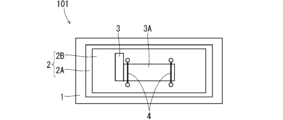
- FIG. 1 is a plan view showing a configuration of a semiconductor device.
- FIG. 1 is a perspective view showing a configuration of a semiconductor device.
- 2 is a flowchart showing a method for manufacturing a semiconductor device in the embodiment.
- FIG. 11 is a front view showing a state in which a fixing wire pattern has been formed.
- FIG. 11 is a plan view showing a state in which a fixing wire pattern is formed.
- FIG. 4 is a front view showing an inserted state of the electrode terminal.
- 13 is a front view showing a state in which the electrode terminal is pressed by the fixing wire pattern.
- FIG. 13 is a plan view showing a state in which an electrode terminal is pressed by a fixing wire pattern.
- FIG. FIG. 11 is a front view showing a configuration of a semiconductor device in a second embodiment.
- FIG. 1 is a plan view showing a configuration of a
- Fig. 1 is a front view showing the configuration of a semiconductor device 101 in the first embodiment.
- Fig. 2 is a plan view showing the configuration of the semiconductor device 101.
- Fig. 3 is a perspective view showing the configuration of the semiconductor device 101 (heat sink 1 is not shown).
- the semiconductor device 101 includes a heat sink 1, an insulating substrate 2, a semiconductor element (not shown), an electrode terminal 3, and a fixing wire pattern 4.
- the heat sink 1 is a plate made of a metal such as copper (Cu) or aluminum (Al), or a plate made of an AlSiC composite material.
- the heat sink 1 has the function of transferring heat generated by electronic components such as semiconductor elements included in the semiconductor device 101 to the outside.
- the insulating substrate 2 is provided on the heat sink 1 via a bonding material 5.
- the bonding material 5 is, for example, solder, brazing material, sintered material, etc.
- the insulating substrate 2 includes a ceramic substrate 2A and a circuit pattern 2B.
- the ceramic substrate 2A is formed of a ceramic material such as alumina (Al 2 O 3 ), aluminum nitride (AlN), silicon nitride (Si 3 N 4 ), etc.
- the circuit pattern 2B is provided on the upper surface of the ceramic substrate 2A.
- the circuit pattern 2B is formed of a conductive material such as aluminum (Al), copper (Cu), or an alloy thereof.
- the semiconductor element is electrically connected to the circuit pattern 2B of the insulating substrate 2.
- the semiconductor element is held by the circuit pattern 2B via, for example, a conductive bonding material (not shown).
- the semiconductor is preferably a so-called wide band gap semiconductor such as SiC, GaN, Ga 2 O 3 , GeO 2 , diamond, etc.
- the semiconductor element is a power semiconductor element, a control IC (Integrated Circuit) for controlling the power semiconductor element, etc.
- the semiconductor element includes, for example, an IGBT (Insulated Gate Bipolar Transistor), a MOSFET (Metal Oxide Semiconductor Field Effect Transistor), a Schottky barrier diode, etc.
- the semiconductor element may include an RC-IGBT (Reverse-Conducting IGBT) in which an IGBT and a free wheel diode are formed in one semiconductor substrate.
- the electrode terminal 3 is, for example, a conductor configured to be connectable to an external circuit provided outside the semiconductor device 101.
- the electrode terminal 3 is, for example, a metal frame formed by processing a metal plate into a predetermined shape.
- the electrode terminal 3 includes a joint 3A.
- the joint 3A is joined to the circuit pattern 2B.
- the joint 3A is directly joined to the circuit pattern 2B by ultrasonic joining.
- the electrode terminal 3 is formed of, for example, aluminum (Al), copper (Cu), or the like.
- the joint 3A that contacts the circuit pattern 2B may be plated with nickel (Ni).
- the fixing wire pattern 4 has a loop shape. Both ends of the fixing wire pattern 4 are bonded to the circuit pattern 2B.
- the fixing wire pattern 4 is raised from the circuit pattern 2B between the both ends, forming a loop shape with respect to the circuit pattern 2B.
- the fixing wire pattern 4 extends in a direction intersecting the extension direction of the electrode terminal 3.
- the fixing wire pattern 4 is provided so as to straddle the joint 3A.
- two fixing wire patterns 4 are provided so as to straddle the tip and base of the joint 3A, respectively.
- the joint 3A is pressed toward the circuit pattern 2B by the fixing wire pattern 4.
- the lower surface of the joint 3A is in surface contact with the circuit pattern 2B.
- the fixing wire pattern 4 is formed, for example, of an aluminum wire (Al wire).
- the fixing wire pattern 4 is formed, for example, by wire bonding.
- FIG. 4 is a flowchart showing a method for manufacturing a semiconductor device 101 according to an embodiment.
- a circuit pattern 2B is prepared.
- an insulating substrate 2 held by a heat sink 1 is prepared.
- the semiconductor element may be bonded to the circuit pattern 2B in advance, or may be bonded later.
- a fixing wire pattern 4 having a loop shape is formed.
- FIG. 5 is a front view showing the state in which the fixing wire pattern 4 has been formed.
- FIG. 6 is a plan view showing the state in which the fixing wire pattern 4 has been formed. Both ends of the fixing wire pattern 4 are bonded to the circuit pattern 2B.
- the fixing wire pattern 4 is formed by wire bonding.
- the fixing wire pattern 4 is formed, for example, so as to extend in the direction of ultrasonic vibration in the process of bonding the joint 3A described below.
- step S3 the electrode terminal 3 is inserted inside the loop shape of the fixing wire pattern 4.
- Figure 7 is a front view showing the inserted state of the electrode terminal 3. Also, Figure 3 shows the state after the insertion of the electrode terminal 3 is completed. Here, the electrode terminal 3 is inserted in a direction perpendicular to the extension direction of the fixing wire pattern 4.
- step S4 the joint 3A is pressed against the circuit pattern 2B by the fixing wire pattern 4.
- the fixing wire pattern 4 is pressed from above and deformed, and this deformation presses the joint 3A against the circuit pattern 2B.
- Figure 8 is a front view showing the state in which the electrode terminal 3 is pressed by the fixing wire pattern 4.
- Figure 9 is a plan view showing the state in which the electrode terminal 3 is pressed by the fixing wire pattern 4. This step S4 holds the joint 3A in surface contact with the circuit pattern 2B.
- step S5 the joint 3A held down by the fixing wire pattern 4 and the circuit pattern 2B are joined by ultrasonic waves.
- the ultrasonic tool applies ultrasonic waves to the top surface of the joint 3A.
- the semiconductor element and other specified components are sealed with a sealing material, and the semiconductor device 101 is completed.
- steps S2 and S3 determine the placement position of the electrode terminal 3 relative to the circuit pattern 2B. This prevents the electrode terminal 3 from shifting out of position.
- steps S4 and S5 ensure that the underside of the joint 3A of the electrode terminal 3 comes into surface contact with the circuit pattern 2B. This prevents gaps from occurring between the circuit pattern 2B and the electrode terminal 3. This reduces the occurrence of defects such as cracks on the underside of the insulating substrate 2 during ultrasonic bonding.
- the semiconductor device 101 in the first embodiment includes a circuit pattern 2B, a fixing wire pattern 4 and an electrode terminal 3.
- the circuit pattern 2B is electrically connected to the semiconductor element.
- the fixing wire pattern 4 has both ends joined to the circuit pattern 2B and is raised above the circuit pattern 2B between the ends, forming a loop shape.
- the electrode terminal 3 includes a joint 3A inserted into the loop shape and joined to the circuit pattern 2B. The joint 3A is pressed towards the circuit pattern 2B by the fixing wire pattern 4.
- Such a semiconductor device 101 suppresses misalignment of the electrode terminal 3 with respect to the circuit pattern 2B and the occurrence of gaps between the circuit pattern 2B and the electrode terminal 3. As a result, the reliability of the semiconductor device 101 is improved.
- the insulating substrate 2 is held to the heat sink 1 via a bonding material 5, and the electrode terminals 3 are bonded to a circuit pattern 2B formed on the ceramic substrate 2A of the insulating substrate 2.
- the configuration of the circuit pattern 2B is not limited to the above.
- An insulating film may be formed on the upper surface of the heat sink 1, and the circuit pattern 2B may be provided on the insulating film. In that case, the insulating film is formed of resin.
- FIG. 10 is a front view showing the configuration of semiconductor device 102 in embodiment 2.
- FIG. 11 is a plan view showing the configuration of semiconductor device 102.
- FIG. 12 is a perspective view showing the configuration of semiconductor device 102 (heat sink 1 is not shown).
- Semiconductor device 102 includes heat sink 1, insulating substrate 2, semiconductor element (not shown), electrode terminal 3, fixing wire pattern 4, and misalignment prevention wire pattern 6.
- a portion of the fixing wire pattern 4 is joined to the upper surface of the joint 3A.
- the portion of the fixing wire pattern 4 joined to the upper surface of the joint 3A is any portion of the fixing wire pattern 4 excluding both ends.
- the joint 3A is pressed toward the circuit pattern 2B by the fixing wire pattern 4. As a result, the lower surface of the joint 3A is in surface contact with the circuit pattern 2B.
- the misalignment prevention wire pattern 6 has a loop shape. Both ends of the misalignment prevention wire pattern 6 are bonded to the circuit pattern 2B, and the wire pattern 6 is raised from the circuit pattern 2B between the ends.
- the misalignment prevention wire pattern 6 is provided along the periphery of the joint 3A. In the second embodiment, two misalignment prevention wire patterns 6 are provided along both sides of the base of the joint 3A.
- the misalignment prevention wire pattern 6 is formed, for example, from an aluminum wire (Al wire).
- the misalignment prevention wire pattern 6 is formed by wire bonding.
- the fixing wire pattern 4 ensures that the underside of the joint 3A of the electrode terminal 3 comes into surface contact with the circuit pattern 2B. This reduces the occurrence of gaps between the circuit pattern 2B and the electrode terminal 3.
- the fixing wire pattern 4 and the misalignment prevention wire pattern 6 hold the joint 3A of the electrode terminal 3 in a specified mounting position. This prevents the electrode terminal 3 from misaligning.
- each embodiment can be freely combined, modified, or omitted as appropriate.
Landscapes
- Wire Bonding (AREA)
Priority Applications (2)
| Application Number | Priority Date | Filing Date | Title |
|---|---|---|---|
| PCT/JP2023/039583 WO2025094349A1 (ja) | 2023-11-02 | 2023-11-02 | 半導体装置および半導体装置の製造方法 |
| JP2025554447A JPWO2025094349A1 (https=) | 2023-11-02 | 2023-11-02 |
Applications Claiming Priority (1)
| Application Number | Priority Date | Filing Date | Title |
|---|---|---|---|
| PCT/JP2023/039583 WO2025094349A1 (ja) | 2023-11-02 | 2023-11-02 | 半導体装置および半導体装置の製造方法 |
Publications (1)
| Publication Number | Publication Date |
|---|---|
| WO2025094349A1 true WO2025094349A1 (ja) | 2025-05-08 |
Family
ID=95582573
Family Applications (1)
| Application Number | Title | Priority Date | Filing Date |
|---|---|---|---|
| PCT/JP2023/039583 Pending WO2025094349A1 (ja) | 2023-11-02 | 2023-11-02 | 半導体装置および半導体装置の製造方法 |
Country Status (2)
| Country | Link |
|---|---|
| JP (1) | JPWO2025094349A1 (https=) |
| WO (1) | WO2025094349A1 (https=) |
Citations (10)
| Publication number | Priority date | Publication date | Assignee | Title |
|---|---|---|---|---|
| JP2001346384A (ja) * | 2000-05-31 | 2001-12-14 | Mitsubishi Electric Corp | パワーモジュール |
| JP2002359334A (ja) * | 2001-05-31 | 2002-12-13 | Toyota Industries Corp | 半導体装置の端子構造 |
| US20070013059A1 (en) * | 2005-07-06 | 2007-01-18 | Ralf Otremba | Semiconductor power module with SIC power diodes and method for its production |
| JP2007027467A (ja) * | 2005-07-19 | 2007-02-01 | Nichicon Corp | 半導体モジュール |
| WO2012073572A1 (ja) * | 2010-12-03 | 2012-06-07 | 富士電機株式会社 | 半導体装置、および、半導体装置の製造方法 |
| JP2017017204A (ja) * | 2015-07-02 | 2017-01-19 | 三菱電機株式会社 | 半導体装置の製造方法 |
| JP2018006576A (ja) * | 2016-07-01 | 2018-01-11 | 三菱電機株式会社 | 半導体装置 |
| WO2018029801A1 (ja) * | 2016-08-10 | 2018-02-15 | 三菱電機株式会社 | 半導体装置 |
| JP2018207002A (ja) * | 2017-06-07 | 2018-12-27 | 三菱電機株式会社 | 半導体装置の製造方法 |
| JP2021077817A (ja) * | 2019-11-13 | 2021-05-20 | 三菱電機株式会社 | 半導体装置 |
-
2023
- 2023-11-02 WO PCT/JP2023/039583 patent/WO2025094349A1/ja active Pending
- 2023-11-02 JP JP2025554447A patent/JPWO2025094349A1/ja active Pending
Patent Citations (10)
| Publication number | Priority date | Publication date | Assignee | Title |
|---|---|---|---|---|
| JP2001346384A (ja) * | 2000-05-31 | 2001-12-14 | Mitsubishi Electric Corp | パワーモジュール |
| JP2002359334A (ja) * | 2001-05-31 | 2002-12-13 | Toyota Industries Corp | 半導体装置の端子構造 |
| US20070013059A1 (en) * | 2005-07-06 | 2007-01-18 | Ralf Otremba | Semiconductor power module with SIC power diodes and method for its production |
| JP2007027467A (ja) * | 2005-07-19 | 2007-02-01 | Nichicon Corp | 半導体モジュール |
| WO2012073572A1 (ja) * | 2010-12-03 | 2012-06-07 | 富士電機株式会社 | 半導体装置、および、半導体装置の製造方法 |
| JP2017017204A (ja) * | 2015-07-02 | 2017-01-19 | 三菱電機株式会社 | 半導体装置の製造方法 |
| JP2018006576A (ja) * | 2016-07-01 | 2018-01-11 | 三菱電機株式会社 | 半導体装置 |
| WO2018029801A1 (ja) * | 2016-08-10 | 2018-02-15 | 三菱電機株式会社 | 半導体装置 |
| JP2018207002A (ja) * | 2017-06-07 | 2018-12-27 | 三菱電機株式会社 | 半導体装置の製造方法 |
| JP2021077817A (ja) * | 2019-11-13 | 2021-05-20 | 三菱電機株式会社 | 半導体装置 |
Also Published As
| Publication number | Publication date |
|---|---|
| JPWO2025094349A1 (https=) | 2025-05-08 |
Similar Documents
| Publication | Publication Date | Title |
|---|---|---|
| US8698289B2 (en) | Semiconductor device, a method of manufacturing the same and an electronic device | |
| CN103035601B (zh) | 在烧结银层上包括扩散焊接层的半导体器件 | |
| JP7352763B1 (ja) | 半導体モジュール | |
| US20230298974A1 (en) | Semiconductor device and method for manufacturing semiconductor device | |
| CN110199579B (zh) | 电子模块以及电子模块的制造方法 | |
| CN107615464A (zh) | 电力用半导体装置的制造方法以及电力用半导体装置 | |
| JP7215206B2 (ja) | 半導体装置の製造方法 | |
| US12315826B2 (en) | Semiconductor device package assemblies with direct leadframe attachment | |
| JP5218009B2 (ja) | 半導体装置 | |
| US20260074448A1 (en) | Transfer molded power modules and methods of manufacture | |
| CN213026110U (zh) | 半导体器件 | |
| JPH09232341A (ja) | 半導体装置 | |
| CN109413886B (zh) | 半导体装置的制造方法及焊接辅助工具 | |
| EP3739624A1 (en) | Semiconductor arrangement with a compressible contact element encapsulated between two carriers and corresponding manufacturing method | |
| TW202238888A (zh) | 半導體裝置 | |
| WO2025094349A1 (ja) | 半導体装置および半導体装置の製造方法 | |
| CN115023804B (zh) | 电子器件和电子器件的制造方法 | |
| JP2018170344A (ja) | 半導体装置および半導体装置の製造方法 | |
| JP7690133B2 (ja) | 半導体装置および半導体装置の製造方法 | |
| JP7570298B2 (ja) | 半導体装置 | |
| JP7657329B2 (ja) | 半導体装置および半導体装置の製造方法 | |
| JP2025147545A (ja) | 半導体装置および半導体装置の製造方法 | |
| KR20250008673A (ko) | 다이를 기판에 소결시키는 방법, 파워 모듈 및 다이를 기판에 점착시키는 방법 | |
| WO2024111058A1 (ja) | 半導体装置および半導体装置の製造方法 | |
| JP2025165118A (ja) | 半導体装置、電気機器及び半導体装置の製造方法 |
Legal Events
| Date | Code | Title | Description |
|---|---|---|---|
| 121 | Ep: the epo has been informed by wipo that ep was designated in this application |
Ref document number: 23957675 Country of ref document: EP Kind code of ref document: A1 |
|
| ENP | Entry into the national phase |
Ref document number: 2025554447 Country of ref document: JP Kind code of ref document: A |
|
| WWE | Wipo information: entry into national phase |
Ref document number: 2025554447 Country of ref document: JP |