WO2025083789A1 - 半導体モジュールの製造方法、半導体モジュール - Google Patents
半導体モジュールの製造方法、半導体モジュール Download PDFInfo
- Publication number
- WO2025083789A1 WO2025083789A1 PCT/JP2023/037604 JP2023037604W WO2025083789A1 WO 2025083789 A1 WO2025083789 A1 WO 2025083789A1 JP 2023037604 W JP2023037604 W JP 2023037604W WO 2025083789 A1 WO2025083789 A1 WO 2025083789A1
- Authority
- WO
- WIPO (PCT)
- Prior art keywords
- conductor plate
- plate
- convex portion
- conductive plate
- conductor
- Prior art date
- Legal status (The legal status is an assumption and is not a legal conclusion. Google has not performed a legal analysis and makes no representation as to the accuracy of the status listed.)
- Pending
Links
Images




Classifications
-
- H—ELECTRICITY
- H10—SEMICONDUCTOR DEVICES; ELECTRIC SOLID-STATE DEVICES NOT OTHERWISE PROVIDED FOR
- H10W—GENERIC PACKAGES, INTERCONNECTIONS, CONNECTORS OR OTHER CONSTRUCTIONAL DETAILS OF DEVICES COVERED BY CLASS H10
- H10W72/00—Interconnections or connectors in packages
Definitions
- the present invention relates to a method for manufacturing a semiconductor module and a semiconductor module.
- Patent Document 1 discloses a power module in which a resin sheet is provided on the surface of a lead frame carrying a semiconductor element opposite the surface on which the semiconductor element is mounted, and the surface is sealed with molded resin, and the surface facing the resin sheet bonded to the lead frame is not covered with molded resin.
- the present invention aims to provide a semiconductor module manufacturing method and a semiconductor module that ensure insulation reliability.
- a method for manufacturing a semiconductor module including a first conductive plate to which multiple semiconductor elements are bonded, a second conductive plate arranged adjacent to the first conductive plate so that their sides face each other, and a sealing member that mold-seals the semiconductor elements, the first conductive plate, and the second conductive plate, comprising forming a plate-shaped member having a convex portion formed along the arrangement direction in which the first conductive plate and the second conductive plate are arranged, cutting the plate-shaped member to form the first conductive plate and the second conductive plate separately, bonding the multiple semiconductor elements to the surface of the first conductive plate opposite the convex portion, sealing with the sealing member so that a portion of the convex portion of the first conductive plate is exposed, or attaching a thermally conductive sheet-shaped member to the portion of the convex portion of the first conductive plate that is exposed after sealing with the sealing member, and deforming the second conductive plate so that the surface of the convex portion formed on the second conductive plate is located inside the sealing member relative to the
- the present invention provides a semiconductor module manufacturing method and a semiconductor module that ensures insulation reliability.
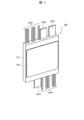
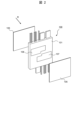
- FIG. 1 is an exploded perspective view of a semiconductor module according to an embodiment of the present invention
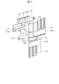
- 1 is a cross-sectional view of a semiconductor module according to an embodiment of the present invention; Partially enlarged view of FIG.
- the semiconductor module 100 is formed by molding and sealing with sealing resin 101, which is a sealing member.
- the semiconductor module 100 has an upper arm control terminal 102A, a P main terminal 102B, an N main terminal 103A, an AC main terminal 104A, and a lower arm control terminal 104B that protrude from the sealing resin 101 to the outside.
- Thermally conductive sheets 105 are bonded to both sides of the semiconductor module 100. In this manner, the semiconductor module 100 and the thermally conductive sheet 105 are integrated.
- FIG. 2 A portion of a surface of a third conductor plate 106 and a portion of a surface of a fifth conductor plate 107, which will be described later, are temporarily bonded to a thermally conductive sheet 105, and then a sealing resin 101 is formed to form a semiconductor module 100.
- the sealing resin 101 is formed along the surface of the thermally conductive sheet 105, the surface of the sealing resin 101 and the exposed surface of a portion of the third conductor plate 106 and the exposed surface of a portion of the fifth conductor plate 107 that are not sealed with the sealing resin 101 are substantially flush with each other.
- the circuit body 200 which is in a state before the semiconductor module 100 described above is sealed with the sealing resin 101, has a first conductor plate 102, a second conductor plate 103, a third conductor plate 106, a fourth conductor plate 104, a fifth conductor plate 107, and a semiconductor element 109.
- the semiconductor element 109 is, for example, a SiC chip or the like, and configures an upper arm circuit and a lower arm circuit.
- the first conductor plate 102, the second conductor plate 103, and the fourth conductor plate 104 are arranged on the same plane.
- the first conductor plate 102 is opposed to the third conductor plate 106 with at least one semiconductor element 109 sandwiched between them, the semiconductor element 109 forming an upper arm circuit electrically in parallel.
- the semiconductor element 109 sandwiched between them is electrically joined to the first conductor plate 102 and the third conductor plate 106 using solder or the like.
- two semiconductor elements 109 are arranged side by side on the first conductor plate 102.
- At least one semiconductor element 109 sandwiched between the first conductor plate 102 and the third conductor plate 106 is arranged on the first conductor plate 102 along the arrangement direction in which the first conductor plate 102 and the second conductor plate 103 are arranged side by side, and then joined to the first conductor plate 102 and the third conductor plate 106.
- the fourth conductor plate 104 faces the fifth conductor plate 107 with at least one semiconductor element 109 (not shown) constituting the lower arm circuit sandwiched therebetween.
- the semiconductor element 109 sandwiched therebetween is electrically joined to the fourth conductor plate 104 and the fifth conductor plate 107 using solder or the like.
- the two semiconductor elements 109 are arranged side by side on the fourth conductor plate 104, similar to the two semiconductor elements 109 arranged on the first conductor plate 102.
- the multiple semiconductor elements 109 arranged on the first conductive plate 102 and the fourth conductive plate 104 are electrically connected to the upper arm control terminal 102A and the lower arm control terminal 104B using aluminum wires or the like (not shown).
- the temperature sensor 108 is disposed on the side of at least one of the first conductive plate 102 and the fourth conductive plate 104 to which the semiconductor element 109 is connected.
- the output terminal of the temperature sensor 108 is connected to at least one of the upper arm control terminal 102A and the lower arm control terminal 104B. In this manner, the temperature sensor 108 detects the temperature of the semiconductor element 109 and outputs a temperature signal.
- FIG. 4 A portion of a surface of the convex portion 102C and a portion of a surface of the convex portion 104C, which will be described later, are temporarily bonded to the thermally conductive sheet 105. Thereafter, the sealing resin 101 is formed to form the semiconductor module 100. After the temporary bonding of the convex portion 102C, the convex portion 104C, and the thermally conductive sheet 105, the sealing resin 101 is formed along the surface of the thermally conductive sheet 105, so that the sealing resin 101, the portion of a surface of the convex portion 102C that is not sealed by the sealing resin 101, and the portion of a surface of the convex portion 104C are substantially flush with each other.
- the surface of the convex portion 102C is exposed to the surface of the sealing resin 101 and the thermally conductive sheet 105 is attached, but for convenience of configuration, it is also possible to leave the surface of the convex portion 102C exposed and not attach the thermally conductive sheet 105.
- first conductor plate 102 By cutting one plate-like member, parts of the cut plate-like member are separated to form the first conductor plate 102, the third conductor plate 106, and the fourth conductor plate 104.
- first conductor plate 102, the third conductor plate 106, and the fourth conductor plate 104 are the same member.
- the first conductor plate 102 and the second conductor plate 103 are disposed adjacent to each other with their side surfaces facing each other.
- the first conductor plate 102 has a convex portion 102C on the surface opposite to the surface to which the multiple semiconductor elements 109 are bonded.
- the second conductor plate 103 has a convex portion 103C that protrudes in the same direction as the protruding direction of the convex portion 102C. Note that the convex portions 102C, 103C are formed along the arrangement direction in which the first conductor plate 102 and the second conductor plate 103 are arranged side by side. In this way, the configuration of the present invention described below can be realized even in a semiconductor module 100 that has a structure in which no separate chip, such as a diode chip, or a conductor plate having a convex shape is installed on the second conductor plate 103.
- a convex portion 104C is provided on the surface opposite to the surface to which the semiconductor element 109 is bonded.
- the convex portion 104C is formed from a convex portion that is formed separately from the convex portion 102C before the separation process, but is located on the same plane as the convex portion 102C on a plane.
- Multiple semiconductor elements 109 are bonded to the surface opposite the convex portion 102C. Additionally, multiple semiconductor elements 109 are bonded to the surface opposite the convex portion 104C.
- the first conductor plate 102, the second conductor plate 103, and the fourth conductor plate 104 are on the same plane when integrally formed from a plate-shaped member, but by forming a bent portion 103D in the second conductor plate 103 and deforming the second conductor plate 103, the convex portion 103C on a plane is positioned inward from the convex portion 102C.
- the third conductor plate 106 and the fifth conductor plate 107 are arranged on the same plane.
- the third conductor plate 106 has a base portion 106B that is electrically connected to at least one semiconductor element 109.
- the fifth conductor plate 107 has a base portion 107B that is electrically connected to at least one semiconductor element 109.
- Figure 6(a) is a cross-sectional view for explaining the connection relationship between the first conductor plate 102, the third conductor plate 106, the fourth conductor plate 104, and the fifth conductor plate 107
- Figure 6(b) is a cross-sectional view of a semiconductor module for explaining the connection relationship between the second conductor plate 103, the fourth conductor plate 104, and the fifth conductor plate 107.
- a convex portion 102C is provided on the surface opposite to the surface to which the semiconductor element 109 is bonded, and the convex portion 102C is exposed from the sealing resin 101.
- a convex portion 104C is provided on the surface opposite to the surface to which the semiconductor element 109 is bonded, and the convex portion 104C is exposed from the sealing resin 101.
- the convex portion 102C exposed from the sealing resin 101 and the convex portion 104C are placed on the same plane and bonded to the thermally conductive sheet 105.
- a pedestal portion 106B is provided on the third conductor plate 106.
- the semiconductor element 109 is sandwiched between the first conductor plate 102 and the pedestal portion 106B and electrically connected to each of them, thereby positioning the third conductor plate 106 in a position opposite the first conductor plate 102.
- a pedestal portion 107B is provided on the fifth conductor plate 107.
- the semiconductor element 109 is sandwiched between the fourth conductor plate 104 and the pedestal portion 107B and electrically connected to each of them.
- the surface of the third conductor plate 106 opposite the surface on which the base portion 106B is provided is exposed from the sealing resin 101.
- the surface of the fifth conductor plate 107 opposite the surface on which the base portion 107B is provided is exposed from the sealing resin 101.
- the surface of the third conductor plate 106 exposed from the sealing resin 101 and the surface of the fifth conductor plate 107 are made to be on the same plane and are bonded to the thermally conductive sheet 105.
- a connection portion 106A is formed on the third conductor plate 106, and the third conductor plate 106 is connected to the fourth conductor plate 104 via the connection portion 106A.
- the fifth conductor plate 107 is provided with a connection portion 107A.
- the fifth conductor plate 107 is electrically connected to the second conductor plate 103 via the connection portion 107A by soldering or the like.
- the second conductor plate 103 is deformed by forming the bent portion 103D so that the surface of the convex portion 103C is located closer to the inside of the sealing resin 101 than the surface of the convex portion 102C.
- the connection portion between the convex portion 103C and the other region is bent after the plate-like member is divided, so that the surface of the convex portion 103C is provided on a different plane from the surface of the convex portion 102C, thereby forming the bent portion 103D.
- the semiconductor module 100 is formed by filling and molding the sealing resin 101.
- the sealing resin 101 is filled, the convex portion 103C is not exposed from the sealing resin 101 and is not bonded to the thermally conductive sheet 105, unlike the convex portion 104C which is exposed from the sealing resin 101 and bonded to the thermally conductive sheet 105.
- the sealing resin 101 is formed between the convex portion 103C and the thermally conductive sheet 105.
- the semiconductor element 109 is sandwiched between the fourth conductor plate 104 and the base portion 107B and electrically connected to it.
- the fourth conductor plate 104 and the base portion 107B are rigidly fixed together via the semiconductor element 109, so when the thermally conductive sheet 105 is bonded to both sides of the structure and a load is applied, the fourth conductor plate 104 and the fifth conductor plate 107 do not deform and can generate the surface pressure required for bonding.
- the first conductor plate 102 and the third conductor plate 106 which faces the semiconductor element 109, are combined to form a rigid structure, and when a load is applied to the thermally conductive sheet 105 from both sides of the structure and the structure is bonded, the first conductor plate 102 and the third conductor plate 106 are able to generate the surface pressure required for bonding without deformation.
- a gap can be provided between the thermally conductive sheet 105 and the sealing resin 101 can be poured in, making it unnecessary to bond the thermally conductive sheet 105 and preventing corona discharge.
- a method for manufacturing a semiconductor module 100 including a first conductive plate 102 to which a plurality of semiconductor elements 109 are joined, a second conductive plate 103 disposed adjacent to the first conductive plate 102 such that their side surfaces face each other, and a sealing member 101 that mold-seals the semiconductor elements 109, the first conductive plate 102, and the second conductive plate 103, the method including forming a plate-like member having a convex portion formed along an arrangement direction in which the first conductive plate 102 and the second conductive plate 103 are arranged side by side, and cutting the plate-like member to separate the first conductive plate 102 and the second conductive plate 103
- a method is adopted in which a plurality of semiconductor elements 109 are joined to the surface of the first conductor plate 102 opposite the convex portion 102C, and a portion of the convex portion 102C of the first conductor plate 102 is exposed on the surface of the sealing member 101, or a thermally conductive sheet 105 is attached to a portion
- the thermally conductive sheet 105 is attached, or after the thermally conductive sheet 105 is bonded in advance under high temperature and high pressure, the thermally conductive sheet 105 is sealed together with the sealing resin 101 with a part of the thermally conductive sheet 105 exposed. In this way, a manufacturing method for the semiconductor module 100 with ensured insulation reliability can be realized.
- connection portion between the convex portion and another region is bent so that the surface of the convex portion provided on the second conductor plate 103 is provided on a different plane from the surface of the convex portion provided on the first conductor plate 102. By doing so, the convex portion 103C is not exposed when the sealing resin 101 is formed.
- a sealing member 101 is formed between the deformed second conductive plate 103 and the sheet-like member 105. By doing so, it is possible to ensure insulation even in the convex portion 103C, which is a portion of the lead frame to which pressure can be applied with a load only from one side.
- a third conductor plate 106 is placed in a position facing the first conductor plate 102 with the semiconductor element 109 in between, and the sealing member 101 is formed by molding and sealing the semiconductor element 109 in a state where it is sandwiched between the first conductor plate 102 and the third conductor plate 106. In this way, sufficient pressure can be generated by applying a load at high temperature and high pressure from both sides.
- a set of semiconductor elements 109 that are electrically parallel is arranged on the surface opposite the convex portion provided on the first conductor plate 102 along the arrangement direction in which the first conductor plate 102 and the second conductor plate 103 are arranged side by side.
- the semiconductor module 100 of the present invention comprises a first conductor plate 102 to which a plurality of semiconductor elements 109 are joined, a second conductor plate 103 arranged adjacent to the first conductor plate 102 with their sides facing each other, and a sealing member 101 that molds and seals the semiconductor elements 109, the first conductor plate 102, and the second conductor plate 103, wherein each of the first conductor plate 102 and the second conductor plate 103 is provided with a convex portion formed along an arrangement direction in which the first conductor plate 102 and the second conductor plate 103 are arranged side by side, a plurality of semiconductor elements 109 are joined to the opposite surface of the convex portion 102C of the first conductor plate 102, a portion of the convex portion 102C of the first conductor plate 102 is exposed on the surface of the sealing member 101, or a thermally conductive sheet-like member 105 is attached to the surface of the extruded sealing member, and the convex portion 103C of the second conductor
- the thermally conductive sheet 105 is attached, or after the thermally conductive sheet 105 is previously attached under high temperature and high pressure, the thermally conductive sheet 105 is sealed together with the thermally conductive sheet 105 with the sealing resin 101 while part of the thermally conductive sheet 105 is exposed. In this way, a semiconductor module 100 with ensured insulation reliability can be provided.
- the present invention is not limited to the above-described embodiment, and various modifications and other configurations can be combined without departing from the spirit of the invention. Furthermore, the present invention is not limited to those having all of the configurations described in the above-described embodiment, and also includes those in which some of the configurations have been omitted.
Landscapes
- Structures Or Materials For Encapsulating Or Coating Semiconductor Devices Or Solid State Devices (AREA)
Priority Applications (3)
| Application Number | Priority Date | Filing Date | Title |
|---|---|---|---|
| PCT/JP2023/037604 WO2025083789A1 (ja) | 2023-10-17 | 2023-10-17 | 半導体モジュールの製造方法、半導体モジュール |
| CN202380101553.3A CN121730031A (zh) | 2023-10-17 | 2023-10-17 | 半导体模块的制造方法、半导体模块 |
| JP2025552514A JPWO2025083789A1 (https=) | 2023-10-17 | 2023-10-17 |
Applications Claiming Priority (1)
| Application Number | Priority Date | Filing Date | Title |
|---|---|---|---|
| PCT/JP2023/037604 WO2025083789A1 (ja) | 2023-10-17 | 2023-10-17 | 半導体モジュールの製造方法、半導体モジュール |
Publications (1)
| Publication Number | Publication Date |
|---|---|
| WO2025083789A1 true WO2025083789A1 (ja) | 2025-04-24 |
Family
ID=95448615
Family Applications (1)
| Application Number | Title | Priority Date | Filing Date |
|---|---|---|---|
| PCT/JP2023/037604 Pending WO2025083789A1 (ja) | 2023-10-17 | 2023-10-17 | 半導体モジュールの製造方法、半導体モジュール |
Country Status (3)
| Country | Link |
|---|---|
| JP (1) | JPWO2025083789A1 (https=) |
| CN (1) | CN121730031A (https=) |
| WO (1) | WO2025083789A1 (https=) |
Citations (5)
| Publication number | Priority date | Publication date | Assignee | Title |
|---|---|---|---|---|
| JPH07147360A (ja) * | 1993-11-25 | 1995-06-06 | Sanyo Electric Co Ltd | 表面実装型半導体装置 |
| JP2001326295A (ja) * | 2000-05-15 | 2001-11-22 | Rohm Co Ltd | 半導体装置および半導体装置製造用フレーム |
| JP2014187149A (ja) * | 2013-03-22 | 2014-10-02 | Hitachi Automotive Systems Ltd | パワーモジュール |
| JP2018142620A (ja) * | 2017-02-28 | 2018-09-13 | 日立オートモティブシステムズ株式会社 | パワー半導体装置 |
| WO2019044177A1 (ja) * | 2017-08-30 | 2019-03-07 | 日立オートモティブシステムズ株式会社 | パワー半導体装置及びその製造方法 |
-
2023
- 2023-10-17 WO PCT/JP2023/037604 patent/WO2025083789A1/ja active Pending
- 2023-10-17 JP JP2025552514A patent/JPWO2025083789A1/ja active Pending
- 2023-10-17 CN CN202380101553.3A patent/CN121730031A/zh active Pending
Patent Citations (5)
| Publication number | Priority date | Publication date | Assignee | Title |
|---|---|---|---|---|
| JPH07147360A (ja) * | 1993-11-25 | 1995-06-06 | Sanyo Electric Co Ltd | 表面実装型半導体装置 |
| JP2001326295A (ja) * | 2000-05-15 | 2001-11-22 | Rohm Co Ltd | 半導体装置および半導体装置製造用フレーム |
| JP2014187149A (ja) * | 2013-03-22 | 2014-10-02 | Hitachi Automotive Systems Ltd | パワーモジュール |
| JP2018142620A (ja) * | 2017-02-28 | 2018-09-13 | 日立オートモティブシステムズ株式会社 | パワー半導体装置 |
| WO2019044177A1 (ja) * | 2017-08-30 | 2019-03-07 | 日立オートモティブシステムズ株式会社 | パワー半導体装置及びその製造方法 |
Also Published As
| Publication number | Publication date |
|---|---|
| CN121730031A (zh) | 2026-03-24 |
| JPWO2025083789A1 (https=) | 2025-04-24 |
Similar Documents
| Publication | Publication Date | Title |
|---|---|---|
| US9455215B2 (en) | Semiconductor device and method for manufacturing the same | |
| TWI404177B (zh) | 功率半導體電路裝置及其製造方法 | |
| US8003446B2 (en) | Flexible diode package and method of manufacturing | |
| US10910326B2 (en) | Semiconductor package | |
| CN103794585B (zh) | 半导体功率转换器及其制造方法 | |
| JP5659938B2 (ja) | 半導体ユニットおよびそれを用いた半導体装置 | |
| JP6899784B2 (ja) | パワー半導体装置 | |
| JP6627600B2 (ja) | パワーモジュールの製造方法 | |
| CN102903693A (zh) | 功率器件封装模块及其制造方法 | |
| US7763906B2 (en) | Semiconductor light-emitting device and method | |
| JP2016105477A (ja) | 基板アダプタを製造する方法、基板アダプタ、および半導体素子を接触させるための方法 | |
| CN102487053A (zh) | 半导体装置及其制造方法 | |
| US5250839A (en) | Multi-layer leadframes, electrically conductive plates used therefor and production of such conductive plates | |
| US8278747B2 (en) | Semiconductor apparatus having a two-side heat radiation structure | |
| JP5733092B2 (ja) | 半導体装置及びその製造方法 | |
| WO2025083789A1 (ja) | 半導体モジュールの製造方法、半導体モジュール | |
| JP2012142466A (ja) | 半導体装置 | |
| JP2007206336A (ja) | 光モジュールおよびその製造方法 | |
| WO2022137701A1 (ja) | 電気回路体および電力変換装置 | |
| JP5946761B2 (ja) | 電極部材及び電極部材の製造方法 | |
| JP4917296B2 (ja) | 半導体装置の製造方法 | |
| JP2012004359A (ja) | 半導体モジュールの積層体 | |
| JP7720918B2 (ja) | 電力用半導体装置および電力用半導体装置の製造方法 | |
| JP2015103670A (ja) | 電力変換装置およびその製造方法 | |
| JP2012238749A (ja) | 半導体装置 |
Legal Events
| Date | Code | Title | Description |
|---|---|---|---|
| 121 | Ep: the epo has been informed by wipo that ep was designated in this application |
Ref document number: 23956040 Country of ref document: EP Kind code of ref document: A1 |
|
| ENP | Entry into the national phase |
Ref document number: 2025552514 Country of ref document: JP Kind code of ref document: A |