WO2025069863A1 - エッチング方法及びプラズマ処理装置 - Google Patents
エッチング方法及びプラズマ処理装置 Download PDFInfo
- Publication number
- WO2025069863A1 WO2025069863A1 PCT/JP2024/030506 JP2024030506W WO2025069863A1 WO 2025069863 A1 WO2025069863 A1 WO 2025069863A1 JP 2024030506 W JP2024030506 W JP 2024030506W WO 2025069863 A1 WO2025069863 A1 WO 2025069863A1
- Authority
- WO
- WIPO (PCT)
- Prior art keywords
- gas
- silicon
- substrate
- etching method
- film
- Prior art date
- Legal status (The legal status is an assumption and is not a legal conclusion. Google has not performed a legal analysis and makes no representation as to the accuracy of the status listed.)
- Pending
Links
Images




Classifications
-
- H—ELECTRICITY
- H10—SEMICONDUCTOR DEVICES; ELECTRIC SOLID-STATE DEVICES NOT OTHERWISE PROVIDED FOR
- H10P—GENERIC PROCESSES OR APPARATUS FOR THE MANUFACTURE OR TREATMENT OF DEVICES COVERED BY CLASS H10
- H10P50/00—Etching of wafers, substrates or parts of devices
- H10P50/20—Dry etching; Plasma etching; Reactive-ion etching
- H10P50/24—Dry etching; Plasma etching; Reactive-ion etching of semiconductor materials
- H10P50/242—Dry etching; Plasma etching; Reactive-ion etching of semiconductor materials of Group IV materials
Definitions
- An exemplary embodiment of the present disclosure relates to an etching method and a plasma processing apparatus.
- U.S. Patent Application Publication No. 2016/0343580 discloses a process gas containing a fluorocarbon gas as a process gas used in plasma etching of a silicon-containing film.
- JP 2016-39310 A discloses a process gas containing a hydrocarbon gas and a hydrofluorocarbon gas as a process gas used in plasma etching of a silicon-containing film.
- This disclosure provides a technology that suppresses shape abnormalities in the sidewalls of recesses formed by etching.
- an etching method includes: (a) a step of carrying a substrate into a chamber of a plasma processing apparatus, the substrate having a silicon-containing film and a mask provided on the silicon-containing film, the silicon-containing film containing at least one element selected from the group consisting of nitrogen, phosphorus, and boron; and (b) a step of exposing the substrate to plasma generated from a processing gas containing hydrogen fluoride gas, the step (b) including a step of forming a recess in the silicon-containing film and a step of forming a protective film containing the at least one element on the sidewall of the recess.
- FIG. 1 is a schematic diagram of a plasma processing apparatus according to an exemplary embodiment.
- FIG. 2 is a schematic diagram of a plasma processing apparatus according to an exemplary embodiment.
- FIG. 3 is a flow chart of an etching method according to one exemplary embodiment.
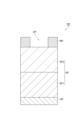
- FIG. 4 is a cross-sectional view of an example substrate to which the method of FIG. 3 may be applied.
- FIG. 5 is a cross-sectional view of another example substrate to which the method of FIG. 3 can be applied.
- FIG. 6 is a cross-sectional view of yet another example substrate to which the method of FIG. 3 can be applied.
- FIG. 7 is a cross-sectional view illustrating a step of an etching method according to an exemplary embodiment.
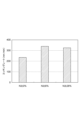
- FIG. 8 is a diagram showing an example of the results of an experiment on the difference in etching rate depending on the ratio of nitrogen contained in a silicon-containing film.
- FIG. 1 is a schematic diagram of a plasma processing apparatus according to an exemplary embodiment.
- the plasma processing system includes a plasma processing apparatus 1 and a control unit 2.
- the plasma processing system is an example of a substrate processing system
- the plasma processing apparatus 1 is an example of a substrate processing apparatus.
- the plasma processing apparatus 1 includes a plasma processing chamber 10, a substrate support unit 11, and a plasma generation unit 12.
- the plasma processing chamber 10 has a plasma processing space.
- the plasma processing chamber 10 also has at least one gas supply port for supplying at least one processing gas to the plasma processing space, and at least one gas exhaust port for exhausting gas from the plasma processing space.
- the gas supply port is connected to a gas supply unit 20 described later, and the gas exhaust port is connected to an exhaust system 40 described later.
- the substrate support unit 11 is disposed in the plasma processing space and has a substrate support surface for supporting a substrate.
- the plasma generating unit 12 is configured to generate plasma from at least one processing gas supplied into the plasma processing space.
- the plasma formed in the plasma processing space may be capacitively coupled plasma (CCP), inductively coupled plasma (ICP), ECR plasma (Electron-Cyclotron-resonance plasma), helicon wave plasma (HWP), or surface wave plasma (SWP), etc.
- various types of plasma generating units may be used, including AC (Alternating Current) plasma generating units and DC (Direct Current) plasma generating units.
- the AC signal (AC power) used in the AC plasma generating unit has a frequency in the range of 100 kHz to 10 GHz.
- AC signals include RF (Radio Frequency) signals and microwave signals.
- the RF signal has a frequency in the range of 100 kHz to 150 MHz.
- the control unit 2 processes computer-executable instructions that cause the plasma processing apparatus 1 to perform the various steps described in this disclosure.
- the control unit 2 may be configured to control each element of the plasma processing apparatus 1 to perform the various steps described herein. In one embodiment, a part or all of the control unit 2 may be included in the plasma processing apparatus 1.
- the control unit 2 may include a processing unit 2a1, a storage unit 2a2, and a communication interface 2a3.
- the control unit 2 is realized, for example, by a computer 2a.
- the processing unit 2a1 may be configured to perform various control operations by reading a program from the storage unit 2a2 and executing the read program. This program may be stored in the storage unit 2a2 in advance, or may be acquired via a medium when necessary.
- the acquired program is stored in the storage unit 2a2 and is read from the storage unit 2a2 by the processing unit 2a1 and executed.
- the medium may be various storage media readable by the computer 2a, or may be a communication line connected to the communication interface 2a3.
- the processing unit 2a1 may be a CPU (Central Processing Unit).
- the memory unit 2a2 may include a RAM (Random Access Memory), a ROM (Read Only Memory), a HDD (Hard Disk Drive), a SSD (Solid State Drive), or a combination of these.
- the communication interface 2a3 may communicate with the plasma processing device 1 via a communication line such as a LAN (Local Area Network).
- FIG. 2 is a schematic diagram of a plasma processing apparatus according to one exemplary embodiment.
- the capacitively coupled plasma processing apparatus 1 includes a plasma processing chamber 10, a gas supply unit 20, a power supply 30, and an exhaust system 40.
- the plasma processing apparatus 1 also includes a substrate support unit 11 and a gas inlet unit.
- the gas inlet unit is configured to introduce at least one processing gas into the plasma processing chamber 10.
- the gas inlet unit includes a shower head 13.
- the substrate support unit 11 is disposed in the plasma processing chamber 10.
- the shower head 13 is disposed above the substrate support unit 11. In one embodiment, the shower head 13 constitutes at least a part of the ceiling of the plasma processing chamber 10.
- the plasma processing chamber 10 has a plasma processing space 10s defined by the shower head 13, the sidewall 10a of the plasma processing chamber 10, and the substrate support unit 11.
- the plasma processing chamber 10 is grounded.
- the shower head 13 and the substrate support unit 11 are electrically insulated from the housing of the plasma processing chamber 10.
- the substrate support 11 includes a main body 111 and a ring assembly 112.
- the main body 111 has a central region 111a for supporting the substrate W and an annular region 111b for supporting the ring assembly 112.
- a wafer is an example of a substrate W.
- the annular region 111b of the main body 111 surrounds the central region 111a of the main body 111 in a plan view.
- the substrate W is disposed on the central region 111a of the main body 111
- the ring assembly 112 is disposed on the annular region 111b of the main body 111 so as to surround the substrate W on the central region 111a of the main body 111. Therefore, the central region 111a is also called a substrate support surface for supporting the substrate W, and the annular region 111b is also called a ring support surface for supporting the ring assembly 112.
- the main body 111 includes a base 1110 and an electrostatic chuck 1111.
- the base 1110 includes a conductive member.
- the conductive member of the base 1110 may function as a lower electrode.
- the electrostatic chuck 1111 is disposed on the base 1110.
- the electrostatic chuck 1111 includes a ceramic member 1111a and an electrostatic electrode 1111b disposed within the ceramic member 1111a.
- the ceramic member 1111a has a central region 111a. In one embodiment, the ceramic member 1111a also has an annular region 111b. Note that other members surrounding the electrostatic chuck 1111, such as an annular electrostatic chuck or an annular insulating member, may have the annular region 111b.
- the ring assembly 112 may be disposed on the annular electrostatic chuck or the annular insulating member, or may be disposed on both the electrostatic chuck 1111 and the annular insulating member.
- at least one RF/DC electrode coupled to an RF power source 31 and/or a DC power source 32 described later may be disposed in the ceramic member 1111a.
- the at least one RF/DC electrode functions as a lower electrode.
- the RF/DC electrode is also called a bias electrode.
- the conductive member of the base 1110 and the at least one RF/DC electrode may function as multiple lower electrodes.
- the electrostatic electrode 1111b may function as a lower electrode.
- the substrate support 11 includes at least one lower electrode.
- the ring assembly 112 includes one or more annular members.
- the one or more annular members include one or more edge rings and at least one cover ring.
- the edge rings are formed of a conductive or insulating material, and the cover rings are formed of an insulating material.
- the substrate support 11 may also include a temperature adjustment module configured to adjust at least one of the electrostatic chuck 1111, the ring assembly 112, and the substrate to a target temperature.
- the temperature adjustment module may include a heater, a heat transfer medium, a flow passage 1110a, or a combination thereof.
- a heat transfer fluid such as brine or a gas flows through the flow passage 1110a.
- the flow passage 1110a is formed in the base 1110, and one or more heaters are disposed in the ceramic member 1111a of the electrostatic chuck 1111.
- the substrate support 11 may also include a heat transfer gas supply configured to supply a heat transfer gas to a gap between the back surface of the substrate W and the central region 111a.
- the gas supply unit 20 may include at least one gas source 21 and at least one flow controller 22.
- the gas supply unit 20 is configured to supply at least one process gas from a respective gas source 21 through a respective flow controller 22 to the showerhead 13.
- Each flow controller 22 may include, for example, a mass flow controller or a pressure-controlled flow controller.
- the gas supply unit 20 may include at least one flow modulation device that modulates or pulses the flow rate of the at least one process gas.
- the power supply 30 includes an RF power supply 31 coupled to the plasma processing chamber 10 via at least one impedance matching circuit.
- the RF power supply 31 is configured to supply at least one RF signal (RF power) to at least one lower electrode and/or at least one upper electrode. This causes a plasma to be formed from at least one processing gas supplied to the plasma processing space 10s.
- the RF power supply 31 can function as at least a part of the plasma generating unit 12.
- a bias RF signal to at least one lower electrode, a bias potential is generated on the substrate W, and ion components in the formed plasma can be attracted to the substrate W.
- the RF power supply 31 includes a first RF generating unit 31a and a second RF generating unit 31b.
- the first RF generating unit 31a is coupled to at least one lower electrode and/or at least one upper electrode via at least one impedance matching circuit and configured to generate a source RF signal (source RF power) for plasma generation.
- the source RF signal has a frequency in the range of 10 MHz to 150 MHz.
- the first RF generating unit 31a may be configured to generate multiple source RF signals having different frequencies. The generated one or more source RF signals are supplied to at least one lower electrode and/or at least one upper electrode.
- the second RF generator 31b is coupled to at least one lower electrode via at least one impedance matching circuit and configured to generate a bias RF signal (bias RF power).
- the frequency of the bias RF signal may be the same as or different from the frequency of the source RF signal.
- the bias RF signal has a lower frequency than the frequency of the source RF signal.
- the bias RF signal has a frequency in the range of 100 kHz to 60 MHz.
- the second RF generator 31b may be configured to generate multiple bias RF signals having different frequencies.
- the generated one or more bias RF signals are provided to at least one lower electrode. Also, in various embodiments, at least one of the source RF signal and the bias RF signal may be pulsed.
- the power supply 30 may also include a DC power supply 32 coupled to the plasma processing chamber 10.
- the DC power supply 32 includes a first DC generator 32a and a second DC generator 32b.
- the first DC generator 32a is connected to at least one lower electrode and configured to generate a first DC signal.
- the generated first DC signal is applied to the at least one lower electrode.
- the second DC generator 32b is connected to at least one upper electrode and configured to generate a second DC signal.
- the generated second DC signal is applied to the at least one upper electrode.
- the first and second DC signals may be pulsed.
- a sequence of voltage pulses is applied to at least one lower electrode and/or at least one upper electrode.
- the voltage pulses may have a rectangular, trapezoidal, triangular or combination thereof pulse waveform.
- a waveform generator for generating a sequence of voltage pulses from the DC signal is connected between the first DC generator 32a and at least one lower electrode.
- the first DC generator 32a and the waveform generator constitute a voltage pulse generator.
- the second DC generator 32b and the waveform generator constitute a voltage pulse generator
- the voltage pulse generator is connected to at least one upper electrode.
- the voltage pulses may have a positive polarity or a negative polarity.
- the sequence of voltage pulses may also include one or more positive polarity voltage pulses and one or more negative polarity voltage pulses within one period.
- the first and second DC generating units 32a and 32b may be provided in addition to the RF power source 31, or the first DC generating unit 32a may be provided in place of the second RF generating unit 31b.
- the exhaust system 40 may be connected to, for example, a gas exhaust port 10e provided at the bottom of the plasma processing chamber 10.
- the exhaust system 40 may include a pressure regulating valve and a vacuum pump. The pressure in the plasma processing space 10s is adjusted by the pressure regulating valve.
- the vacuum pump may include a turbomolecular pump, a dry pump, or a combination thereof.
- FIG. 3 is a flow chart of an etching method according to one exemplary embodiment.
- the etching method MT shown in FIG. 3 (hereinafter referred to as "method MT") can be performed by the plasma processing apparatus 1 of the above embodiment.
- Method MT can be applied to a substrate W.
- FIG. 4 is a cross-sectional view of an example substrate W to which method MT can be applied.
- the substrate W shown in FIG. 4 is used in the manufacture of devices such as DRAMs and 3D-NANDs.
- the substrate W has a silicon-containing film SF.
- the substrate W may further have an underlayer region UR.
- the silicon-containing film SF may be provided on the underlayer region UR.
- the underlayer region UR may contain a material different from the material contained in the silicon-containing film SF.
- the underlayer region UR may contain silicon.
- the silicon-containing film SF contains at least one element (hereinafter also referred to as an additive element) selected from the group consisting of nitrogen (N), phosphorus (P), and boron (B).
- the silicon-containing film SF may contain nitrogen and at least one element selected from the group consisting of phosphorus and boron.
- the silicon-containing film SF may contain at least one selected from the group consisting of a silicon nitride film and a silicon oxynitride film.
- the silicon-containing film SF may contain a silicon oxide film containing an additive element.
- the silicon-containing film SF may include a multilayer film containing alternately stacked silicon oxide films and silicon nitride films. In this case, the silicon oxide film may contain an additive element, and the silicon nitride film may contain at least one element selected from the group consisting of phosphorus and boron.
- the additive element may be doped during the formation of the silicon-containing film SF.
- a gas containing the additive element may be included in the source gas.
- the additive element may be doped after the silicon-containing film SF is formed.
- the additive element may be doped into the silicon-containing film SF by ion implantation.
- the ratio of the additive element contained in the silicon-containing film SF may be 10 atomic % or less.
- the ratio of the additive element may be 8 atomic % or less.
- the ratio of the additive element may be 6 atomic % or less.
- the ratio of the additive element may be 1 atomic % or more.
- the ratio of the additive element may be 2 atomic % or more.
- the ratio of the additive element may be 0.5 atomic % or more.
- the ratio of the additive element may be the sum of the atomic % of each element.
- the atomic percentage may be the ratio of the mass of the added element to the total mass of the silicon-containing film SF divided by the atomic weight of the added element. For example, if a silicon nitride film contains 95 mass% silicon and 5 mass% nitrogen, the value obtained by dividing 95 mass% by 28, which is the atomic weight of silicon, is 3.39. The value obtained by dividing 5 mass% by 14.1, which is the atomic weight of nitrogen, is 0.35. When these values are expressed as percentages, the atomic percentage of silicon is 90.6 atomic% and the atomic percentage of nitrogen is 9.4 atomic%.
- the atomic percentage can be measured, for example, by secondary ion mass spectrometry (SIMS) or X-ray photoelectron spectroscopy (XPS).
- SIMS secondary ion mass spectrometry
- XPS X-ray photoelectron spectroscopy
- the substrate W further includes a mask MK.
- the mask MK may have an opening OP.
- the opening OP may have a hole pattern or a line pattern.
- the mask MK may be provided on the silicon-containing film SF.
- the mask MK may include at least one selected from the group consisting of silicon, carbon, and a metal.
- the mask MK may include at least one selected from the group consisting of a silicon-containing film different from the silicon-containing film SF, a carbon-containing film, and a metal-containing film.
- the silicon-containing film different from the silicon-containing film SF may include a polysilicon film.
- the carbon-containing film may include an amorphous carbon film.
- the metal-containing film may include at least one metal selected from the group consisting of tungsten (W), titanium (Ti), and ruthenium (Ru).
- FIG. 5 is a cross-sectional view of another example of a substrate W1 to which the method MT can be applied.
- the silicon-containing film SF may include a first region SF1 and a second region SF2.
- the first region SF1 may include the additive element in a first ratio
- the second region SF2 may include the additive element in a second ratio different from the first ratio.
- the second ratio may be smaller than the first ratio or larger than the first ratio.
- the first ratio and the second ratio may be in the atomic percentages described above.
- the second region SF2 is provided on the first region SF1 in the thickness direction of the substrate W1.
- FIG. 6 is a cross-sectional view of yet another example of a substrate W2 to which the method MT can be applied.
- the second region SF2 may be aligned with the first region SF1 in the in-plane direction of the substrate W2.
- the in-plane direction of the substrate W2 is a direction perpendicular to the thickness direction of the substrate W2.
- the opening OP of the mask MK may include a first opening OP1 and a second opening OP2.
- the mask MK may have a first opening OP1 on the first region SF1 and a second opening OP2 on the second region SF2.
- the shape of the first opening OP1 and the shape of the second opening OP2 are different from each other.
- the first opening OP1 may be a hole-shaped opening.
- the second opening OP2 may be a slit-shaped opening.
- the second ratio in the second region SF2 in which the slit-shaped opening is formed may be different from the first ratio in the first region SF1 in which the hole-shaped opening is formed.
- the method MT will be described below with reference to Figures 4 and 7, taking as an example the case where the method MT is applied to a substrate W using the plasma processing apparatus 1 of the above embodiment. In the following description, the method MT will be described as being applied to a substrate W, but the method MT may also be applied to a substrate W1 or substrate W2 instead of the substrate W.
- FIGs 4 and 7 is a cross-sectional view showing one step of an etching method according to one exemplary embodiment.
- the method MT can be performed in the plasma processing apparatus 1 by controlling each part of the plasma processing apparatus 1 by the control unit 2.
- a substrate W on a substrate support 11 arranged in a plasma processing chamber 10 is processed as shown in Figure 2.
- method MT may include steps ST1 and ST2. Steps ST1 and ST2 may be performed in sequence.
- Step ST1 4 is loaded into the plasma processing chamber 10 by, for example, a transfer device.
- the substrate W may be supported by a substrate support 11 in the plasma processing chamber 10.
- the substrate W having the silicon-containing film SF doped with an additive element is loaded into the plasma processing chamber 10.
- Step ST2 in step ST2, a plasma PL is generated from a processing gas, and the substrate W is exposed to the plasma PL.
- Step ST2 includes a step (step ST21) of forming a recess RE in the silicon-containing film SF by etching, and a step (step ST22) of forming a protective film DP containing an additive element on a side wall REa of the recess RE.
- Step ST21 and step ST22 may be performed simultaneously, or step ST22 may be performed after step ST21.
- a recess RE is formed in the silicon-containing film SF by etching.
- the recess RE corresponds to the opening OP.
- the processing gas includes fluorine (F) and hydrogen (H).
- the processing gas includes, for example, hydrogen fluoride.
- the plasma PL includes a hydrogen fluoride (HF) etchant, and the recess RE is formed by etching the silicon-containing film SF with the hydrogen fluoride etchant.
- the hydrogen fluoride etchant may include hydrogen fluoride active species and neutral molecules of hydrogen fluoride.
- the hydrogen fluoride active species may include hydrogen fluoride ions and hydrogen fluoride radicals.
- a hydrogen fluoride etchant having an H-F bond is generated.
- the hydrogen fluoride etchant may be detected, for example, by a quadrupole mass spectrometer (QMS).
- the hydrogen fluoride etchant may be detected, for example, by a solid-state optical emission spectrometer (OES).
- OES optical emission spectrometer
- a window (not shown) may be provided in the side wall 10a of the plasma processing chamber 10, and the emission spectrum of the plasma PL obtained from the window may be analyzed qualitatively and quantitatively.
- the window may be a glass plate, and may be fitted, for example, into a through hole connecting the inside and outside of the plasma processing chamber 10.
- the processing gas may contain a gas of a compound containing hydrogen and fluorine, or may be a mixed gas containing a hydrogen-containing gas and a fluorine-containing gas.
- the gas of the compound containing hydrogen and fluorine may contain at least one selected from the group consisting of hydrogen fluoride gas and hydrofluorocarbon gas (C x H y F z gas). Each of x, y, and z is a positive integer.
- the hydrogen fluoride gas and the hydrofluorocarbon gas may generate a hydrogen fluoride etchant in the plasma PL.
- the hydrofluorocarbon gas may be at least one selected from the group consisting of CHF3 , CH2F2 , CH3F , C2HF5 , C2H2F4 , C2H3F3 , C2H4F2 , C3HF7 , C3H2F2 , C3H2F6 , C3H2F4 , C3H3F5 , C4H5F5 , C4H2F6 , C5H2F10 , c - C5H3F7 , and C3H2F4 .
- the hydrogen-containing gas contained in the mixed gas may include at least one selected from the group consisting of H2 gas, NH3 gas, H2O gas, H2O2 gas, and a hydrocarbon gas.
- the fluorine-containing gas contained in the mixed gas may include at least one selected from NF3 gas, SF6 gas, WF6 gas, XeF2 gas, a fluorocarbon gas, and a hydrofluorocarbon gas.
- the mixed gas may generate a hydrogen fluoride etchant in the plasma PL.
- the processing gas may include at least one selected from the group consisting of a nitrogen-containing gas, a phosphorus-containing gas, a carbon-containing gas, a gas containing a halogen other than fluorine, a boron-containing gas, and an oxygen-containing gas.
- the nitrogen-containing gas may include at least one selected from the group consisting of nitrogen gas ( N2 gas), an oxynitride gas ( NO gas), a nitrogen trifluoride gas ( NF3 gas), an ammonia gas ( NH3 gas), a mixed gas of nitrogen gas and hydrogen gas, and an amine gas.
- the phosphorus-containing gas may include at least one selected from the group consisting of phosphorus trifluoride gas (PF3 gas) and phosphorus pentafluoride gas ( PF5 gas).
- the carbon-containing gas may include at least one selected from the group consisting of fluorocarbon gas ( CxFy gas ) and hydrofluorocarbon gas .
- the fluorocarbon gas may be at least one selected from the group consisting of CF4 , C2F2 , C2F4 , C3F8 , C4F6 , C4F8 , and C5F8 .
- the hydrofluorocarbon gas may be at least one selected from CHF3, CH2F2, CH3F, C2HF5, C2H2F4, C2H3F3, C2H4F2, C3HF7, C3H2F2, C3H2F6, C3H2F4, C3H3F5, C4H5F5 , C4H2F6 , C5H2F10 , c - C5H3F7 , and C3H2F4 .
- the halogen - containing gas other than fluorine may include at least one selected from the group consisting of a chlorine - containing gas and a bromine - containing gas .
- the chlorine-containing gas may include Cl2 gas.
- the bromine-containing gas may include HBr gas.
- the boron-containing gas may include boron trichloride gas ( BCl3 gas).
- the oxygen-containing gas may include at least one selected from the group consisting of oxygen gas ( O2 ), carbon monoxide gas (CO), and carbon dioxide gas ( CO2 ).
- the temperature of the substrate support part 11 that supports the substrate W may be set to 0°C or lower, -40°C or lower, -60°C or lower, or -80°C or higher.
- an electrical bias may be supplied to the substrate support part 11.
- a protective film DP may be formed on the bottom surface REb, or the protective film DP may not be formed on the bottom surface REb.
- the mechanism by which the formation of the recesses on the bottom surface REb proceeds is, for example, as follows, but is not limited to this.
- hydrogen fluoride ions are incident on the substrate W along the thickness direction of the substrate W. This removes the protective film DP formed on the bottom surface REb, and etching proceeds on the exposed bottom surface REb.
- the protective film DP remains on the side wall REa, where hydrogen fluoride ions are less likely to be incident.
- the protective film DP prevents hydrogen fluoride radicals from entering the side wall REa, so that the formation of the recesses proceeds preferentially on the bottom surface REb, and anisotropic etching is achieved.
- the protective film DP formed on the side wall REa in the process ST22 may be generated by a reaction between the chemical species in the plasma PL and the silicon-containing film SF containing an additive element.
- the silicon-containing film SF contains nitrogen
- the hydrogen fluoride etchant contained in the process gas reacts with the silicon-containing film SF to generate an ammonium salt.
- the protective film DP may contain an ammonium salt.
- the ammonium salt may contain ammonium silicofluoride.
- the ammonium salt may contain at least one selected from the group consisting of (NH 4 ) 2 SiF 6 , NH 4 SiF 5 , and (NH 4 ) 3 SiF 7.
- the protective film DP may contain a phosphate.
- the phosphate may contain ammonium hexafluorophosphate (NH 4 PF 6 ).
- a borate may be generated by reacting the silicon-containing film SF with chemical species in the plasma PL. Therefore, the protective film DP may contain a borate.
- the borate may contain ammonium tetrafluoroborate (NH 4 BF 4 ).
- the additive element contained in the silicon-containing film SF promotes the adsorption of hydrogen fluoride species to the silicon-containing film SF.
- a protective film DP is formed on the sidewall REa of the recess RE by a reaction between the silicon-containing film SF containing the additive element and the hydrogen fluoride species.
- the protective film DP suppresses the penetration of hydrogen fluoride radicals in the hydrogen fluoride species into the sidewall REa, thereby suppressing etching of the sidewall REa of the recess RE. This makes it possible to suppress shape abnormalities (bowing) of the sidewall REa of the recess RE.
- the protective film DP is difficult to form on the bottom surface REb of the recess RE due to collision of hydrogen fluoride ions in the hydrogen fluoride species, so etching is promoted.
- the additive element contained in the silicon-containing film SF promotes the adsorption of hydrogen fluoride species to the bottom surface REb of the recess RE, so the etching rate of the silicon-containing film SF can be increased.
- a recess RE can be formed from the second region SF2 to the first region SF1.
- the second region SF2 is provided on the first region SF1 in the thickness direction of the substrate W1.
- the second ratio may be greater than the first ratio.
- the higher the ratio of the additive element the more the adsorption of the hydrogen fluoride etchant is promoted, and the thickness of the protective film DP attached to the side wall REa of the recess RE tends to be thicker.
- the protective film DP formed on the side wall REa in the second region SF2 can be made thicker.
- the second ratio may be smaller than the first ratio. In this case, adsorption of hydrogen fluoride species to the bottom surface REb of the recess RE formed in the first region SF1 is promoted. This makes it possible to increase the etching rate of the first region SF1. This makes it possible to suppress the etching rate of the silicon-containing film SF from decreasing the farther it is from the mask MK.
- a recess RE may be formed in each of the first region SF1 and the second region SF2.
- the second region SF2 is aligned with the first region SF1 in the in-plane direction of the substrate W2.
- the mask MK may have a hole-shaped opening (first opening OP1) on the first region SF1 and a slit-shaped opening (second opening OP2) on the second region SF2.
- the second ratio in the second region SF2 in which the slit-shaped opening is formed may be different from the first ratio in the first region SF1 in which the hole-shaped opening is formed.
- the second ratio When the second ratio is larger than the first ratio, the etching rate of the second region SF2 can be increased. When the second ratio is smaller than the first ratio, the etching rate of the first region SF1 can be increased. Therefore, by making the first ratio different from the second ratio, the difference between the etching rate of the first region SF1 and the etching rate of the second region SF2 can be adjusted. For example, the second ratio may be greater than the first ratio.
- the second region SF2 in which the slit-shaped opening is formed often includes a silicon oxide film.
- the first region SF1 in which the hole-shaped opening is formed often includes a silicon nitride film or a silicon oxynitride film.
- the etching rate for the silicon oxide film tends to be smaller than the etching rate for the silicon nitride film or the silicon oxynitride film. Therefore, by making the second ratio greater than the first ratio, the etching rate of the second region SF2 can be increased. As a result, the difference between the etching rate of the first region SF1 and the etching rate of the second region SF2 can be reduced.
- the silicon-containing film SF and the mask MK may contain an additive element.
- the mask MK contains an additive element
- the additive element contained in the mask MK may adhere to the sidewall REa of the recess RE formed in the silicon-containing film SF by etching the mask MK.
- a protective film DP is formed on the sidewall REa of the recess RE of the silicon-containing film SF by a reaction between the sidewall REa to which the additive element is attached and the hydrogen fluoride species.
- Figure 8 shows an example of the results of an experiment on the difference in etching rate depending on the ratio of nitrogen contained in the silicon-containing film SF.
- a substrate containing a silicon-containing film to be etched was prepared.
- substrate samples a first sample was prepared in which the silicon oxide film was not doped with nitrogen, a second sample was doped with nitrogen at a ratio of 6 atomic %, and a third sample was doped with nitrogen at a ratio of 28 atomic %.
- the silicon-containing film of each sample was formed by plasma-enhanced chemical vapor deposition (PECVD). After the substrate was carried into a plasma processing chamber, the film to be etched was etched by plasma generated from a processing gas. Hydrogen fluoride gas was used as the processing gas.
- PECVD plasma-enhanced chemical vapor deposition
- the etching rates of the second and third samples doped with nitrogen were about 1.5 times that of the first sample not doped with nitrogen. From this result, it was found that the doping of nitrogen promoted the adsorption of hydrogen fluoride species to the silicon-containing film, improving the etching rate. On the other hand, it was found that there was no significant difference between the etching rate of the second sample doped with nitrogen at a ratio of 6 atomic % and the etching rate of the third sample doped with nitrogen at a ratio of 28 atomic %. In other words, it was found that the effect of the ratio of nitrogen on the etching rate was small, and that the inclusion of nitrogen in the silicon-containing film at a small ratio had the effect of improving the etching rate.
- [E1] (a) loading a substrate into a chamber of a plasma processing apparatus, the substrate having a silicon-containing film and a mask disposed on the silicon-containing film, the silicon-containing film containing at least one element selected from the group consisting of nitrogen, phosphorus, and boron; (b) exposing the substrate to a plasma generated from a process gas including hydrogen fluoride gas; Including, The step (b) includes forming a recess in the silicon-containing film, and forming a protective film containing the at least one element on a side wall of the recess. Etching method.
- the silicon-containing film comprises nitrogen;
- the silicon-containing film comprises nitrogen;
- the second region is provided on the first region in a thickness direction of the substrate, The etching method according to [E7], wherein the second ratio is greater than the first ratio.
- the second region is provided on the first region in a thickness direction of the substrate, The etching method according to [E7], wherein the second ratio is smaller than the first ratio.
- the second region is aligned with the first region in an in-plane direction of the substrate,
- the etching method according to [E7], wherein the mask has a hole-shaped opening in the first region and a slit-shaped opening in the second region.
- [E14] (a) carrying a substrate into a chamber of a plasma processing apparatus, the substrate having a silicon-containing film and a mask provided on the silicon-containing film, at least one of the silicon-containing film and the mask containing at least one element selected from the group consisting of nitrogen, phosphorus, and boron; (b) exposing the substrate to a plasma generated from a process gas comprising fluorine and hydrogen; Including, The step (b) includes forming a recess in the silicon-containing film and forming a protection film containing the at least one element on a side wall of the recess; the plasma includes a hydrogen fluoride etchant; Etching method.
- a plasma processing apparatus comprising: A chamber; a substrate support for supporting a substrate in the chamber, the substrate having a silicon-containing film and a mask provided on the silicon-containing film, the silicon-containing film including at least one element selected from the group consisting of nitrogen, phosphorus, and boron; a gas supply configured to supply a process gas including hydrogen fluoride gas into the chamber; a plasma generating unit configured to generate plasma from the processing gas; A control unit; Equipped with The control unit is (a) loading the substrate into the chamber; (b) exposing the substrate to the plasma, the step including the steps of forming a recess in the silicon-containing film and forming a protection film including the at least one element on a side wall of the recess; 13.
- a plasma processing apparatus configured to control the plasma processing apparatus to perform an etching method including:
- 1...plasma processing device 10...plasma processing chamber, 11...substrate support, 12...plasma generation unit, 2...control unit, 20...gas supply unit, DP...protective film, MK...mask, PL...plasma, RE...recess, REa...sidewall, SF...silicon-containing film, W...substrate.
Landscapes
- Drying Of Semiconductors (AREA)
Priority Applications (2)
| Application Number | Priority Date | Filing Date | Title |
|---|---|---|---|
| CN202480059445.9A CN121890303A (zh) | 2023-09-28 | 2024-08-27 | 蚀刻方法及等离子体处理装置 |
| JP2025548628A JP7836946B2 (ja) | 2023-09-28 | 2024-08-27 | エッチング方法及びプラズマ処理装置 |
Applications Claiming Priority (2)
| Application Number | Priority Date | Filing Date | Title |
|---|---|---|---|
| JP2023-167773 | 2023-09-28 | ||
| JP2023167773 | 2023-09-28 |
Publications (1)
| Publication Number | Publication Date |
|---|---|
| WO2025069863A1 true WO2025069863A1 (ja) | 2025-04-03 |
Family
ID=95202499
Family Applications (1)
| Application Number | Title | Priority Date | Filing Date |
|---|---|---|---|
| PCT/JP2024/030506 Pending WO2025069863A1 (ja) | 2023-09-28 | 2024-08-27 | エッチング方法及びプラズマ処理装置 |
Country Status (4)
| Country | Link |
|---|---|
| JP (1) | JP7836946B2 (https=) |
| CN (1) | CN121890303A (https=) |
| TW (1) | TW202529200A (https=) |
| WO (1) | WO2025069863A1 (https=) |
Citations (6)
| Publication number | Priority date | Publication date | Assignee | Title |
|---|---|---|---|---|
| JPH0677177A (ja) * | 1992-06-22 | 1994-03-18 | Matsushita Electric Ind Co Ltd | ドライエッチング法及びドライエッチング装置 |
| CN108321211A (zh) * | 2017-01-16 | 2018-07-24 | 中芯国际集成电路制造(上海)有限公司 | Tmbs半导体器件及其制作方法、电子装置 |
| JP2018529225A (ja) * | 2015-08-31 | 2018-10-04 | レール・リキード−ソシエテ・アノニム・プール・レテュード・エ・レクスプロワタシオン・デ・プロセデ・ジョルジュ・クロード | 半導体構造物をエッチングするための窒素含有化合物 |
| WO2021171764A1 (ja) * | 2020-02-27 | 2021-09-02 | 株式会社日立ハイテク | プラズマ処理方法 |
| JP2023063526A (ja) * | 2021-04-28 | 2023-05-09 | 東京エレクトロン株式会社 | エッチング方法及びプラズマ処理装置 |
| US20230230840A1 (en) * | 2022-01-18 | 2023-07-20 | Samsung Electronics Co., Ltd. | Process gas for cryogenic etching, plasma etching apparatus, and method of fabricating semiconductor device using the same |
Family Cites Families (1)
| Publication number | Priority date | Publication date | Assignee | Title |
|---|---|---|---|---|
| JP7700221B2 (ja) | 2021-05-07 | 2025-06-30 | 東京エレクトロン株式会社 | 基板処理方法及び基板処理装置 |
-
2024
- 2024-08-27 JP JP2025548628A patent/JP7836946B2/ja active Active
- 2024-08-27 WO PCT/JP2024/030506 patent/WO2025069863A1/ja active Pending
- 2024-08-27 CN CN202480059445.9A patent/CN121890303A/zh active Pending
- 2024-08-29 TW TW113132533A patent/TW202529200A/zh unknown
Patent Citations (6)
| Publication number | Priority date | Publication date | Assignee | Title |
|---|---|---|---|---|
| JPH0677177A (ja) * | 1992-06-22 | 1994-03-18 | Matsushita Electric Ind Co Ltd | ドライエッチング法及びドライエッチング装置 |
| JP2018529225A (ja) * | 2015-08-31 | 2018-10-04 | レール・リキード−ソシエテ・アノニム・プール・レテュード・エ・レクスプロワタシオン・デ・プロセデ・ジョルジュ・クロード | 半導体構造物をエッチングするための窒素含有化合物 |
| CN108321211A (zh) * | 2017-01-16 | 2018-07-24 | 中芯国际集成电路制造(上海)有限公司 | Tmbs半导体器件及其制作方法、电子装置 |
| WO2021171764A1 (ja) * | 2020-02-27 | 2021-09-02 | 株式会社日立ハイテク | プラズマ処理方法 |
| JP2023063526A (ja) * | 2021-04-28 | 2023-05-09 | 東京エレクトロン株式会社 | エッチング方法及びプラズマ処理装置 |
| US20230230840A1 (en) * | 2022-01-18 | 2023-07-20 | Samsung Electronics Co., Ltd. | Process gas for cryogenic etching, plasma etching apparatus, and method of fabricating semiconductor device using the same |
Also Published As
| Publication number | Publication date |
|---|---|
| JPWO2025069863A1 (https=) | 2025-04-03 |
| CN121890303A (zh) | 2026-04-17 |
| TW202529200A (zh) | 2025-07-16 |
| JP7836946B2 (ja) | 2026-03-27 |
Similar Documents
| Publication | Publication Date | Title |
|---|---|---|
| WO2023058582A1 (ja) | エッチング方法及びエッチング装置 | |
| US20240355589A1 (en) | Etching method and plasma processing apparatus | |
| JP7565194B2 (ja) | エッチング方法及びプラズマ処理装置 | |
| US12272526B2 (en) | Substrate processing method and substrate processing apparatus | |
| JP2023127546A (ja) | プラズマ処理方法及びプラズマ処理装置 | |
| JP7836946B2 (ja) | エッチング方法及びプラズマ処理装置 | |
| KR102751653B1 (ko) | 기판 처리 방법 및 기판 처리 장치 | |
| US12033864B2 (en) | Substrate processing method and substrate processing apparatus | |
| WO2022244678A1 (ja) | 基板処理方法及び基板処理装置 | |
| KR20260061277A (ko) | 에칭 방법 및 플라즈마 처리 장치 | |
| US20250210371A1 (en) | Substrate processing method and substrate processing apparatus | |
| TW202443687A (zh) | 蝕刻方法及電漿處理裝置 | |
| JP2024114273A (ja) | エッチング方法及びエッチング装置 | |
| US20240203698A1 (en) | Etching method and plasma processing apparatus | |
| JP7785422B2 (ja) | エッチング方法及びプラズマ処理装置 | |
| WO2025150427A1 (ja) | エッチング方法及びプラズマ処理システム | |
| JP2024088589A (ja) | エッチング方法及びプラズマ処理装置 | |
| TW202533313A (zh) | 蝕刻方法及電漿處理裝置 | |
| TW202533314A (zh) | 電漿處理方法及電漿處理裝置 | |
| JP2023171269A (ja) | エッチング方法及びプラズマ処理システム | |
| JP2024098961A (ja) | エッチング方法及びプラズマ処理装置 | |
| WO2025234350A1 (ja) | エッチング方法及びプラズマ処理装置 | |
| WO2024247825A1 (ja) | プラズマ処理装置及びプラズマ処理方法 | |
| JP2024176159A (ja) | プラズマ処理方法及びプラズマ処理装置 | |
| JP2026002318A (ja) | エッチング方法及びプラズマ処理装置 |
Legal Events
| Date | Code | Title | Description |
|---|---|---|---|
| 121 | Ep: the epo has been informed by wipo that ep was designated in this application |
Ref document number: 24871664 Country of ref document: EP Kind code of ref document: A1 |
|
| ENP | Entry into the national phase |
Ref document number: 2025548628 Country of ref document: JP Kind code of ref document: A |
|
| WWE | Wipo information: entry into national phase |
Ref document number: 2025548628 Country of ref document: JP |