WO2025041281A1 - 試験装置および試験方法 - Google Patents
試験装置および試験方法 Download PDFInfo
- Publication number
- WO2025041281A1 WO2025041281A1 PCT/JP2023/030205 JP2023030205W WO2025041281A1 WO 2025041281 A1 WO2025041281 A1 WO 2025041281A1 JP 2023030205 W JP2023030205 W JP 2023030205W WO 2025041281 A1 WO2025041281 A1 WO 2025041281A1
- Authority
- WO
- WIPO (PCT)
- Prior art keywords
- under test
- device under
- voltage
- test
- measurement
- Prior art date
- Legal status (The legal status is an assumption and is not a legal conclusion. Google has not performed a legal analysis and makes no representation as to the accuracy of the status listed.)
- Pending
Links
Images

Classifications
-
- G—PHYSICS
- G01—MEASURING; TESTING
- G01R—MEASURING ELECTRIC VARIABLES; MEASURING MAGNETIC VARIABLES
- G01R31/00—Arrangements for testing electric properties; Arrangements for locating electric faults; Arrangements for electrical testing characterised by what is being tested not provided for elsewhere
- G01R31/28—Testing of electronic circuits, e.g. by signal tracer
- G01R31/2851—Testing of integrated circuits [IC]
- G01R31/2855—Environmental, reliability or burn-in testing
- G01R31/2872—Environmental, reliability or burn-in testing related to electrical or environmental aspects, e.g. temperature, humidity, vibration, nuclear radiation
- G01R31/2879—Environmental, reliability or burn-in testing related to electrical or environmental aspects, e.g. temperature, humidity, vibration, nuclear radiation related to electrical aspects, e.g. to voltage or current supply or stimuli or to electrical loads
-
- G—PHYSICS
- G01—MEASURING; TESTING
- G01R—MEASURING ELECTRIC VARIABLES; MEASURING MAGNETIC VARIABLES
- G01R1/00—Details of instruments or arrangements of the types included in groups G01R5/00 - G01R13/00 and G01R31/00
- G01R1/20—Modifications of basic electric elements for use in electric measuring instruments; Structural combinations of such elements with such instruments
- G01R1/206—Switches for connection of measuring instruments or electric motors to measuring loads
-
- G—PHYSICS
- G01—MEASURING; TESTING
- G01R—MEASURING ELECTRIC VARIABLES; MEASURING MAGNETIC VARIABLES
- G01R1/00—Details of instruments or arrangements of the types included in groups G01R5/00 - G01R13/00 and G01R31/00
- G01R1/30—Structural combination of electric measuring instruments with basic electronic circuits, e.g. with amplifier
-
- G—PHYSICS
- G01—MEASURING; TESTING
- G01R—MEASURING ELECTRIC VARIABLES; MEASURING MAGNETIC VARIABLES
- G01R31/00—Arrangements for testing electric properties; Arrangements for locating electric faults; Arrangements for electrical testing characterised by what is being tested not provided for elsewhere
- G01R31/26—Testing of individual semiconductor devices
- G01R31/2601—Apparatus or methods therefor
-
- G—PHYSICS
- G01—MEASURING; TESTING
- G01R—MEASURING ELECTRIC VARIABLES; MEASURING MAGNETIC VARIABLES
- G01R31/00—Arrangements for testing electric properties; Arrangements for locating electric faults; Arrangements for electrical testing characterised by what is being tested not provided for elsewhere
- G01R31/28—Testing of electronic circuits, e.g. by signal tracer
- G01R31/2832—Specific tests of electronic circuits not provided for elsewhere
- G01R31/2834—Automated test systems [ATE]; using microprocessors or computers
-
- G—PHYSICS
- G01—MEASURING; TESTING
- G01R—MEASURING ELECTRIC VARIABLES; MEASURING MAGNETIC VARIABLES
- G01R31/00—Arrangements for testing electric properties; Arrangements for locating electric faults; Arrangements for electrical testing characterised by what is being tested not provided for elsewhere
- G01R31/28—Testing of electronic circuits, e.g. by signal tracer
- G01R31/2851—Testing of integrated circuits [IC]
- G01R31/2855—Environmental, reliability or burn-in testing
- G01R31/286—External aspects, e.g. related to chambers, contacting devices or handlers
- G01R31/2868—Complete testing stations; systems; procedures; software aspects
- G01R31/287—Procedures; Software aspects
-
- G—PHYSICS
- G01—MEASURING; TESTING
- G01R—MEASURING ELECTRIC VARIABLES; MEASURING MAGNETIC VARIABLES
- G01R31/00—Arrangements for testing electric properties; Arrangements for locating electric faults; Arrangements for electrical testing characterised by what is being tested not provided for elsewhere
- G01R31/28—Testing of electronic circuits, e.g. by signal tracer
- G01R31/2851—Testing of integrated circuits [IC]
- G01R31/2882—Testing timing characteristics
Definitions
- the first measurement unit may measure a value corresponding to a current flowing through the device under test of the test subject in response to the application of the first voltage from the first power supply, or may measure a value corresponding to a voltage generated in the device under test of the test subject in response to the flow of the first current from the first power supply.
- 1 shows a test system 1 according to a first embodiment. The operation of the test device 2 will be described. 4 shows operational waveforms of the test device 2. 1 shows a test system 1A according to a second embodiment. 4 shows the operating waveforms of the test device 2A. 22 illustrates an example computer 2200 in which aspects of the present invention may be embodied, in whole or in part.
- First Embodiment 1 shows a test system 1 according to the present embodiment.
- the test system 1 includes a plurality of devices under test 10 and a test apparatus 2.
- the devices under test 10 are referred to as DUTs (Device Under Test).
- Each device under test 10 is an electronic device to be tested by the test apparatus 2.
- Each device under test 10 may be, for example, an integrated circuit including a semiconductor, a discrete semiconductor element, or another type of device.
- Each device under test 10 may have at least one connection terminal 101 that is connected to the test apparatus 2.
- Each device under test 10 may further have another connection terminal (not shown) that is connected to a ground voltage.
- Test device 2 The test apparatus 2 tests each device under test 10.
- the test apparatus 2 may test the quality of electrical static characteristics of each device under test 10 that has been connected in advance.
- the test apparatus 2 may sequentially switch between a device under test 10 as a test target among a plurality of devices under test 10 (in the present embodiment, n devices under test 10 (where n is a natural number of 2 or more) as an example).
- the order of the devices under test 10 may be set according to the connection positions to the test apparatus 2.
- the device under test 10 at one end may be the first device under test 10
- the device under test 10 at the other end may be the nth device under test 10.
- the test device 2 has a constant voltage generating current measuring unit 20, a first switch unit 21, a second voltage source 23, a second switch unit 24, a constant current generating voltage measuring unit 25, a third switch unit 26, a judgment unit 27, and a test controller 28.
- the constant voltage generating current measuring section 20 measures a value corresponding to a current flowing through the device under test 10 in response to application of a constant voltage to the device under test 10.
- the constant voltage generating current measuring section 20 has a first voltage source 201, an amplifier 202, and a current sensor 203.
- the amplifier 202 is provided between the first voltage source 201 and the current sensor 203 to configure a voltage follower circuit.
- the output terminal of the amplifier 202 is connected to the current sensor 203, and is also connected to an inverting input terminal via the current sensor 203.
- the gain of the amplifier 202 may be 1 (0 dB), and the first voltage output from the first voltage source 201 may be output from the output terminal.
- the current sensor 203 is provided between the output terminal of the amplifier 202 and the first switch section 21.
- the current sensor 203 is an example of a first measurement section, and measures electrical characteristics of the device under test 10 in response to the first voltage source 201 being connected to the device under test 10.
- the current sensor 203 may measure a value corresponding to a current flowing through the device under test 10 in response to the application of a first voltage from the first voltage source 201.
- the current sensor 203 measures the current itself flowing between the output terminal of the amplifier 202 and the first switch section 21, but the measurement may be performed at another position, or another value corresponding to the current (for example, a voltage generated across a resistor in response to the current) may be measured.
- the current sensor 203 may supply the measurement value to the judgment section 27.
- the first switch section 21 is provided between the constant voltage generating current measuring section 20 and the n number of devices under test 10.
- the first switch section 21 connects the connection terminal 101 of the device under test 10 to be tested, among the connection terminals 101 of the n number of devices under test 10, to the first voltage source 201.
- the first switch section 21 may alternatively connect the connection terminal 101 of the device under test 10 to be tested to the first voltage source 201.
- the first switch section 21 may have n number of switches 210, one end of which is connected to the output terminal of the amplifier 202 in the constant voltage generating current measuring section 20 and the other end of which is connected to each of the connection terminals 101 of the n number of devices under test 10.
- the other end of the Nth switch 210 (where N is a natural number such that 1 ⁇ N ⁇ n) of the n number of switches 210 may be connected to the connection terminal 101 of the Nth device under test 10.
- Each switch 210 may be controlled by a test controller 28 described later.
- the second voltage source 23 outputs a second voltage of a predetermined magnitude.
- the second voltage source 23 may output the second voltage of a predetermined magnitude to the connection terminal 101 of at least one other device under test 10 other than the device under test 10 to be tested among the n devices under test 10.
- the second voltage source 23 according to the present embodiment may output the second voltage to at least one device under test 10 other than the device under test to be tested, in cooperation with the second switch section 24.
- the device under test 10 from which the second voltage is output may include, among the n devices under test 10, a device under test 10 that is measured by the current sensor 203 after the device under test 10 being tested, or may include a device under test 10 that is measured before the device under test 10 being tested, or may include a device under test 10 that is placed near the device under test 10 being tested.
- the device under test 10 from which the second voltage is output may be each of the n-1 devices under test 10 that are different from the device under test 10 being tested, among the n devices under test 10.
- the second voltage source 23 may output the second voltage in parallel with the measurement by the current sensor 203, and may output a voltage over the measurement period by the current sensor 203.
- the second voltage source 23 may be an amplifier that amplifies the first voltage output from the first voltage source 201 with a preset gain, and may output a voltage in parallel with the voltage output by the first voltage source 201.
- the amplifier as the second voltage source 23 may be connected to the amplifier 202 of the constant voltage generating current measuring unit 20 to form a voltage follower circuit, and may have a gain of 1 (0 dB).
- the second voltage may be a voltage for passing a current through a device under test 10 other than the test subject to settle the device under test 10 to a standby potential, that is, a standby voltage.
- the second voltage may be a voltage closer to the first voltage than the ground voltages of the n devices under test 10, and in this embodiment, as an example, may be a voltage the same magnitude as the first voltage.
- the current path flowing in the test apparatus 2 due to the voltage from the second voltage source 23 may be insulated from the path of the current flowing in the test apparatus 2 due to the voltage from the first voltage source 201.
- the second voltage source 23 is an amplifier, so the input side and the output side are insulated.
- the current path between the second voltage source 23 and each device under test 10 that is not the test subject, and the current path between the first voltage source 201 and the device under test 10 that is the test subject are separate paths that have no common parts and are insulated from each other.
- the second switch section 24 may connect the constant current generation voltage measurement section 25 to the connection terminal 101 of the device under test 10 that is the subject of testing by the constant current generation voltage measurement section 25 when the constant current generation voltage measurement section 25 described below performs a measurement.
- the second switch section 24 may alternatively connect the device under test 10 that is the subject of testing to the constant current generation voltage measurement section 25 when the constant current generation voltage measurement section 25 performs a measurement.
- the second switch section 24 may have n switches 240, each having one end connected to the second voltage source 23 and the other end connected to each of the connection terminals 101 of the n devices under test 10. Of the n switches 240, the other end of the Nth switch 240 may be connected to the connection terminal 101 of the Nth device under test 10. Each switch 240 may be controlled by the test controller 28.
- the wiring from the Nth switch 240 to the Nth device under test 10 in the second switch section 24 and the wiring from the Nth switch 210 to the Nth device under test 10 in the first switch section 21 may have a common wiring portion.
- a noise removal filter such as a smoothing capacitor may be provided in the common wiring portion.
- a board-like interface for connecting between the test apparatus 2 and each device under test 10 may be provided between the n devices under test 10 and the n switches 210 and 240.
- the constant current generation voltage measuring section 25 is an example of a second measuring section, and is connected between the second voltage source 23 and the second switch section 24.
- the constant current generation voltage measuring section 25 measures a value corresponding to a voltage generated in the device under test 10 in response to a current of a predetermined magnitude being passed through the device under test 10.
- the constant current generation voltage measuring section 25 may perform the measurement at a timing different from the measurement timing by the current sensor 203, and may perform the measurement in a state in which the device under test 10 to be tested by the constant current generation voltage measuring section 25 and the constant current generation voltage measuring section 25 are connected by the second switch section 24.
- the current of the predetermined magnitude may be set arbitrarily according to the characteristics of the device under test 10.
- the constant current generation voltage measuring section 25 may have a current source (not shown) that passes a constant current through the device under test 10 to be tested via the second switch section 24.
- the constant current generating voltage measuring section 25 may have a sensor (a voltage sensor, for example) not shown that measures a value corresponding to a voltage generated in the device under test 10 to be tested in response to a current from a current source and supplies the value to the judging section 27.
- the constant current generating voltage measuring section 25 may measure another value corresponding to the voltage (for example, a current flowing in response to a voltage) instead of the voltage itself generated in the device under test 10 to be tested.
- the third switch section 26 is provided between the second voltage source 23 and the constant current generation voltage measurement section 25, and the second switch section 24.
- the third switch section 26 has a switch 261 provided between the constant current generation voltage measurement section 25 and the second switch section 24, and a switch 262 provided between the second voltage source 23 and the second switch section 24.
- the switch 261 may be turned on when the constant voltage generation current measurement section 20 performs measurement, that is, when the current sensor 203 performs measurement, and the switch 262 may be turned on when the constant current generation voltage measurement section 25 performs measurement.
- the test controller 28 controls each section of the test apparatus 2 to execute a test on each device under test 10.
- the test controller 28 may cause the first voltage source 201 and the second voltage source 23 to output a voltage, and may cause the first switch section 21 and the second switch section 24 to switch the connection state between the first voltage source 201 and the second voltage source 23 and the device under test 10, respectively, to be measured by the current sensor 203.
- the test controller 28 may cause the constant current generation voltage measurement section 25 to output a current, and may cause the second switch section 24 to switch the connection state between the constant current generation voltage measurement section 25 and the device under test 10, to be measured by the constant current generation voltage measurement section 25.
- the test controller 28 may be realized by software being executed by a processor or the like.
- the second voltage is output to the connection terminal 101 of the device under test 10 other than the test subject, so that the device under test 10 other than the test subject can be settled to a predetermined potential and put into a standby state for testing.
- a first voltage is applied to a defective device under test 10 to be tested, charge may move between the wiring from the first switch section 21 to the device under test 10 to be tested and the wiring from the first switch section 21 to the device under test 10 not to be tested through the capacitance between the wiring.
- the transfer of charge is eliminated in advance by outputting the second voltage, thereby lowering the impedance of the wiring to the device under test 10 other than the test subject, making it less susceptible to the effects of disturbances and coupling between the wiring, and putting the device under test 10 other than the test subject into a standby state for testing in advance. Furthermore, even if the device under test 10 is a capacitive load and needs to be charged in order to perform a test, the device under test 10 can be charged in advance by outputting the second voltage, and a device under test 10 other than the test subject can be placed in a standby state for testing. This makes it possible to speed up the start of testing for each device under test 10.
- the current path from the second voltage source 23 to the device under test 10 other than the test subject and the current path from the first voltage source 201 to the device under test 10 to be tested are separate paths, even when the current sensor 203 measures a value corresponding to a minute current, a non-minute current can be passed through the current path from the second voltage source 23 to the device under test 10 other than the test subject. Therefore, each device under test 10 can be put into a test standby state early.
- the second voltage is output in parallel with the measurement by the current sensor 203, a device under test 10 other than the device under test 10 under test can be put into a standby state while the device under test 10 under test is being tested. This makes it possible to reliably speed up the start of testing for each device under test 10.
- the second voltage source 23 is selectively connected to each of the connection terminals 101 of at least one device under test 10 other than the test subject, so that the second voltage can be applied to the device under test 10 other than the test subject while preventing the second voltage from being applied to the device under test 10 that is the test subject.
- the devices under test 10 to which the second voltage is applied include the device under test 10 that is to be measured next after the device under test 10 being tested. Therefore, the device under test 10 that is to be measured next can be placed in a test standby state, and the start of testing for that device under test 10 can be accelerated.
- the test apparatus 2 can be formed.
- the second voltage source 23 is an amplifier that amplifies the first voltage from the first voltage source 201, the input side and output side of the second voltage source 23 can be insulated. This makes it possible to prevent a decrease in measurement accuracy caused by the current from the first voltage source 201 flowing to the second voltage source 23 side.
- the second voltage is the same as the first voltage, a device under test 10 other than the test subject can be placed in a standby state so that testing can be performed immediately.
- the second voltage is closer to the first voltage than the ground voltage of the device under test 10
- a device under test 10 other than the test subject can be reliably placed in a standby state for testing.
- (Operation of Test Apparatus 2) 2 shows the operation of the test apparatus 2. Note that this figure shows the operation of the test apparatus 2 relating to the measurement of the constant voltage generation current measurement section 20.
- the test apparatus 2 may test each device under test 10 by performing the processes of steps S10 to S26. In this operation, the first voltage source 201 and the second voltage source may continue to output voltages.
- the second switch section 24 connects the second voltage source 23 to the connection terminal 101 of at least one other device under test 10 (each device under test 10 is used as an example in this embodiment) that is different from the device under test 10 being tested. This allows a second voltage (a voltage having the same magnitude as the first voltage as an example in this embodiment) to be output to the connection terminal 101 of each device under test 10.
Landscapes
- Engineering & Computer Science (AREA)
- Physics & Mathematics (AREA)
- General Physics & Mathematics (AREA)
- General Engineering & Computer Science (AREA)
- Environmental & Geological Engineering (AREA)
- Computer Hardware Design (AREA)
- Microelectronics & Electronic Packaging (AREA)
- Health & Medical Sciences (AREA)
- Toxicology (AREA)
- Testing Of Individual Semiconductor Devices (AREA)
- Testing Electric Properties And Detecting Electric Faults (AREA)
- Tests Of Electronic Circuits (AREA)
Abstract
Description
[先行技術文献]
[特許文献]
[特許文献1]特開2005-300495号公報
[特許文献2]特開2010-190768号公報
図1は、本実施形態に係る試験システム1を示す。試験システム1は、複数の被試験デバイス10と、試験装置2とを備える。なお、図中では被試験デバイス10をDUT(Device Under Test)として記載している。
各被試験デバイス10は、試験装置2によって試験されるエレクトロニクスデバイスである。各被試験デバイス10は、例えば半導体を含む集積回路であってもよいし、ディスクリート型の半導体素子であってもよいし、他の種類のデバイスであってもよい。
試験装置2は、各被試験デバイス10の試験を行う。試験装置2は、予め接続された各被試験デバイス10の電気的な静特性の良否を試験してよい。試験装置2は、複数の被試験デバイス10(本実施形態では一例としてn個(但しnは2以上の自然数)の被試験デバイス10)のうち、何れかの被試験デバイス10を試験対象として順次、切り替えて試験を行ってよい。被試験デバイス10の順番は、試験装置2に対する接続位置に従って設定されてよく、n個の被試験デバイス10が一列に並んで試験装置2と接続される場合には、一端の被試験デバイス10が第1の被試験デバイス10とされ、他端の被試験デバイス10が第nの被試験デバイス10とされてよい。
定電圧発生電流測定部20は、試験対象の被試験デバイス10に定電圧を印加したことに応じて当該被試験デバイス10に流れる電流に応じた値を測定する。定電圧発生電流測定部20は、第1電圧源201と、アンプ202と、電流センサ203とを有する。
第1電圧源201は、第1電源の一例であり、予め定められた大きさの第1電圧を出力する。第1電圧源201は、アンプ202の非反転入力端子に第1電圧を供給してよい。第1電圧は、試験対象の被試験デバイス10に電流を流して測定を行うための電圧、つまり測定用の電圧であってよい。第1電圧の大きさは被試験デバイス10の特性に応じて任意に設定されてよい。本図では一例として、第1電圧源201をバッテリとして図示しているが、整流器やコンバータなど、他の装置であってもよい。
アンプ202は、第1電圧源201と電流センサ203との間に設けられてボルテージフォロワ回路を構成する。アンプ202の出力端子は電流センサ203に接続されるとともに、当該電流センサ203を介して反転入力端子に接続される。アンプ202のゲインは1(0dB)であってよく、第1電圧源201から出力される第1電圧を出力端子から出力してよい。
電流センサ203は、アンプ202の出力端子と、第1スイッチ部21との間に設けられる。電流センサ203は、第1測定部の一例であり、第1電圧源201が試験対象の被試験デバイス10に接続されることに応じた当該被試験デバイス10の電気的特性を測定する。電流センサ203は、第1電圧源201から第1電圧が印加されることに応じて試験対象の被試験デバイス10に流れる電流に応じた値を測定してよい。本実施形態では一例として、電流センサ203は、アンプ202の出力端子と第1スイッチ部21との間に流れる電流そのものを測定するが、他の位置で測定を行ってもよいし、電流に応じた他の値(例えば電流に応じて抵抗の両端に生じる電圧など)を測定してもよい。電流センサ203は、測定値を判定部27に供給してよい。
第1スイッチ部21は、定電圧発生電流測定部20と、n個の被試験デバイス10との間に設けられる。第1スイッチ部21は、n個の被試験デバイス10の接続端子101のうち試験対象の被試験デバイス10の接続端子101を第1電圧源201に対して接続する。第1スイッチ部21は、試験対象の被試験デバイス10の接続端子101を択一的に第1電圧源201に接続してよい。第1スイッチ部21は、それぞれ一端が定電圧発生電流測定部20におけるアンプ202の出力端子に接続され、他端がn個の被試験デバイス10のそれぞれの接続端子101に接続されたn個のスイッチ210を有してよい。n個のスイッチ210のうち、第N(但しNは1≦N≦nの自然数)のスイッチ210の他端は、第Nの被試験デバイス10の接続端子101に接続されてよい。各スイッチ210は、後述のテストコントローラ28によって制御されてよい。
第2電圧源23は、予め定められた大きさの第2電圧を出力する。第2電圧源23は、n個の被試験デバイス10のうち試験対象の被試験デバイス10とは異なる他の少なくとも1つの被試験デバイス10の接続端子101に対して予め定められた大きさの第2電圧を出力してよい。本実施形態に係る第2電圧源23は、第2スイッチ部24と協働して、試験対象とは異なる少なくとも1つの被試験デバイス10に第2電圧を出力してよい。
第2スイッチ部24は、第2電圧源23と、n個の被試験デバイス10との間に設けられる。第2スイッチ部24は、定電圧発生電流測定部20が測定を行うときに、定電圧発生電流測定部20による試験対象とは別の被試験デバイス10の接続端子101のそれぞれに対して第2電圧源23を選択的に接続する。本実施形態では一例として、第2スイッチ部24は、試験対象ではないn-1個の各被試験デバイス10の接続端子101を第2電圧源に接続してよい。
定電流発生電圧測定部25は、第2測定部の一例であり、第2電圧源23と、第2スイッチ部24との間に接続される。定電流発生電圧測定部25は、予め定められた大きさの電流が試験対象の被試験デバイス10に流されることに応じて当該被試験デバイス10に生じる電圧に応じた値を測定する。定電流発生電圧測定部25は、電流センサ203による測定タイミングとは異なるタイミングで測定を行ってよく、定電流発生電圧測定部25による試験対象の被試験デバイス10と当該定電流発生電圧測定部25とが第2スイッチ部24により接続された状態で測定を行ってよい。予め定められた大きさの電流は、被試験デバイス10の特性に応じて任意に設定されてよい。定電流発生電圧測定部25は、第2スイッチ部24を介して試験対象の被試験デバイス10に定電流を流す不図示の電流源を有してよい。定電流発生電圧測定部25は、電流源からの電流に応じて試験対象の被試験デバイス10に生じる電圧に応じた値を測定して判定部27に供給する不図示のセンサ(一例として電圧センサ)を有してよい。なお、定電流発生電圧測定部25は、試験対象の被試験デバイス10に生じる電圧そのものではなく、当該電圧に応じた他の値(例えば電圧に応じて流れる電流など)を測定してもよい。
第3スイッチ部26は、第2電圧源23および定電流発生電圧測定部25と、第2スイッチ部24との間に設けられる。第3スイッチ部26は、定電流発生電圧測定部25および第2スイッチ部24の間に設けられたスイッチ261と、第2電圧源23および第2スイッチ部24の間に設けられたスイッチ262とを有する。スイッチ261は、定電圧発生電流測定部20が測定を行う場合、つまり電流センサ203が測定を行う場合にオンとなってよく、スイッチ262は、定電流発生電圧測定部25が測定を行う場合にオンとなってよい。
判定部27は、定電圧発生電流測定部20による測定結果に基づいて試験対象の被試験デバイス10の良否を判定する。本実施形態に係る判定部27は、定電圧発生電流測定部20および定電流発生電圧測定部25による測定結果に基づいて試験対象の被試験デバイス10の良否を判定してよい。一例として、判定部27は、定電圧発生電流測定部20による測定結果に基づいて試験対象の被試験デバイス10が正常と判定され、かつ、定電流発生電圧測定部25による測定結果に基づいて試験対象の被試験デバイス10が正常と判定されることに応じて、当該被試験デバイス10を良好と判定し、他の場合には被試験デバイス10を不良と判定してよい。なお、判定部27は、定電圧発生電流測定部20による測定結果のみに基づいて被試験デバイス10の良否を判定してもよい。
テストコントローラ28は、試験装置2の各部を制御して各被試験デバイス10に対する試験を実行する。例えば、テストコントローラ28は、第1電圧源201および第2電圧源23から電圧を出力させつつ第1スイッチ部21および第2スイッチ部24によって第1電圧源201および第2電圧源23のそれぞれと被試験デバイス10との接続状態を切り替えて、試験対象の被試験デバイス10に流れる電流を電流センサ203により測定させてよい。テストコントローラ28は、定電流発生電圧測定部25から電流を出力させつつ第2スイッチ部24によって当該定電流発生電圧測定部25と被試験デバイス10との接続状態を切り替えて、試験対象の被試験デバイス10に生じる電圧を定電流発生電圧測定部25に測定させてよい。なお、テストコントローラ28は、ソフトウェアがプロセッサ等で実行されることにより実現されてよい。
以上の試験装置2によれば、試験対象とは別の被試験デバイス10の接続端子101に対して第2電圧が出力されるので、試験対象とは別の被試験デバイス10を予め定められた電位にセトリングし、試験の待機状態とすることができる。例えば、不良な試験対象の被試験デバイス10に第1電圧が印加されて試験が行われると、第1スイッチ部21から当該試験対象の被試験デバイス10までの配線と、第1スイッチ部21から試験対象ではない被試験デバイス10までの配線との間で、配線間の容量を通して電荷が移動しうる。このような場合であっても、第2電圧の出力によって予め電荷の移動を解消して試験対象とは別の当該被試験デバイス10までの配線のインピーダンスを下げ、外乱や配線間の結合の影響を受け難くすると共に、試験対象とは別の当該被試験デバイス10を予め試験の待機状態とすることができる。また、被試験デバイス10が容量性の負荷であり、試験を行うために被試験デバイス10に対して電荷のチャージを行う必要がある場合であっても、第2電圧の出力によって予め電荷のチャージを行い、試験対象とは別の被試験デバイス10を試験の待機状態とすることができる。従って、各被試験デバイス10に対する試験の開始を早めることができる。
図2は、試験装置2の動作を示す。なお、本図では試験装置2の動作のうち、定電圧発生電流測定部20の測定に関する動作を示す。試験装置2は、ステップS10~26の処理を行うことにより各被試験デバイス10の試験を行ってよい。本動作においては第1電圧源201および第2電圧源が電圧を出力し続けてよい。
図3は、試験装置2の動作波形を示す。なお、本図では試験装置2の動作のうち、定電圧発生電流測定部20による測定動作の波形を示す。図中、横軸は時間を示す。「SW_1」~「SW_n」の動作波形は第1スイッチ部21における第1のスイッチ210~第nのスイッチ210に対する制御信号を示し、ハイレベルがオン、ローレベルがオフを示す。「SW_1G」~「SW_nG」の動作波形は第2スイッチ部24における第1のスイッチ240~第nのスイッチ240に対する制御信号を示し、ハイレベルがオン、ローレベルがオフを示す。「印加電圧」の動作波形は第1電圧源201および第2電圧源23から出力される電圧を示す。測定タイミングは、電流センサ203による測定タイミングを示す。
図4は、本実施形態に係る試験システム1Aを示す。なお、本実施形態に係る試験システム1Aにおいて、図1に示された試験システム1の構成と略同一のものには同一の符号を付け、説明を省略する。
図5は、試験装置2Aの動作波形を示す。図中、横軸は時間を示す。「SW_1」~「SW_n」の動作波形は第1スイッチ部21における第1のスイッチ210~第nのスイッチ210に対する制御信号を示し、ハイレベルがオン、ローレベルがオフを示す。「印加電圧」の動作波形は第1電圧源201および第2電圧源23から出力される電圧を示す。測定タイミングは、電流センサ203による測定タイミングを示す。
なお、上記の実施形態においては、第2電圧源23は第1電圧源201と同じ大きさの電圧を出力することとして説明したが、異なる大きさの電圧を出力してもよい。この場合であっても、試験対象とは別の被試験デバイス10を予め定められた電位にセトリングし、試験の待機状態とすることができるため、各被試験デバイス10に対する試験の開始を早めることができる。
2 試験装置
10 被試験デバイス
20 定電圧発生電流測定部
21 第1スイッチ部
23 第2電圧源
24 第2スイッチ部
25 定電流発生電圧測定部
26 第3スイッチ部
27 判定部
28 テストコントローラ
101 接続端子
201 第1電圧源
202 アンプ
203 電流センサ
210 スイッチ
240 スイッチ
245 配線
261 スイッチ
262 スイッチ
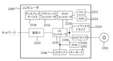
2200 コンピュータ
2201 DVD-ROM
2210 ホストコントローラ
2212 CPU
2214 RAM
2216 グラフィックコントローラ
2218 ディスプレイデバイス
2220 入/出力コントローラ
2222 通信インターフェイス
2224 ハードディスクドライブ
2226 DVD-ROMドライブ
2230 ROM
2240 入/出力チップ
2242 キーボード
Claims (15)
- 予め定められた大きさの第1電圧、または、予め定めれらた大きさの第1電流を出力する第1電源と、
複数の被試験デバイスの接続端子のうち試験対象の被試験デバイスの接続端子を前記第1電源に対して接続する第1スイッチ部と、
前記第1電源が前記試験対象の被試験デバイスに接続されることに応じた当該試験対象の被試験デバイスの電気的特性を測定する第1測定部と、
前記複数の被試験デバイスのうち前記試験対象の被試験デバイスとは異なる他の少なくとも1つの被試験デバイスの前記接続端子に対して予め定められた大きさの第2電圧を出力する第2電圧源と、
を備える試験装置。 - 前記第2電圧源と前記他の少なくとも1つの被試験デバイスとの間の電流経路、および、前記第1電源と前記試験対象の被試験デバイスとの間の電流経路は、互いに別々の経路である、請求項1に記載の試験装置。
- 前記第2電圧源は、前記第1測定部による測定と並行して電圧を出力する、請求項1に記載の試験装置。
- 前記他の少なくとも1つの被試験デバイスの接続端子のそれぞれに対して前記第2電圧源を選択的に接続する第2スイッチ部をさらに備える、請求項1に記載の試験装置。
- 前記他の少なくとも1つの被試験デバイスは、前記複数の被試験デバイスのうち、前記第1測定部によって前記試験対象の被試験デバイスの次に測定が行われる被試験デバイスを含む、請求項4に記載の試験装置。
- 前記第1測定部は、前記第1電源から前記第1電圧が印加されることに応じて前記試験対象の被試験デバイスに流れる電流に応じた値を測定し、
当該試験装置は、前記第1測定部による測定タイミングとは異なるタイミングで、予め定められた大きさの電流が流されることに応じて試験対象の被試験デバイスに生じる電圧に応じた値を測定する第2測定部をさらに備え、
前記第2測定部は、前記第2電圧源と、前記第2スイッチ部との間に接続され、
前記第2スイッチ部は、前記第2測定部が測定を行うときに、前記第2測定部による試験対象の被試験デバイスに前記第2測定部を接続する、請求項4に記載の試験装置。 - 前記第2電圧源と、前記複数の被試験デバイスの接続端子のそれぞれとを接続した各配線に設けられた複数の抵抗をさらに備える、請求項1に記載の試験装置。
- 前記第1測定部は、前記第1スイッチ部が前記試験対象の被試験デバイスを前記第1電源に対して接続していない状態における測定値に応じて、前記第1スイッチ部が前記試験対象の被試験デバイスを前記第1電源に対して接続している状態における測定値を調整する、請求項7に記載の試験装置。
- 前記第1電源は、予め定められた第1電圧を出力し、
前記第2電圧源は、前記第1電源から出力される第1電圧を予め設定されたゲインで増幅するアンプである、請求項1に記載の試験装置。 - 前記第1電源は、予め定められた第1電圧を出力し、
前記第2電圧は、前記第1電圧と同じ大きさの電圧である、請求項1に記載の試験装置。 - 前記第1電源は、予め定められた第1電圧を出力し、
前記第2電圧は、前記複数の被試験デバイスのグランド電圧よりも、前記第1電圧に近い電圧である、請求項1に記載の試験装置。 - 前記第2電圧源が前記他の少なくとも1つの被試験デバイスに流す電流は、前記第1電源が前記試験対象の被試験デバイスに流す電流よりも大きい、請求項1に記載の試験装置。
- 前記第1測定部による測定結果に基づいて前記試験対象の被試験デバイスの良否を判定する判定部をさらに備え、
前記判定部は、前記第1電源を前記試験対象の被試験デバイスに対して接続してから基準時間内に前記第1測定部による測定結果の値の変化速度が基準値以下とならないことに応じて、当該試験対象の被試験デバイスを不良と判定する、請求項1に記載の試験装置。 - 前記第1測定部は、前記第1電源から前記第1電圧が印加されることに応じて前記試験対象の被試験デバイスに流れる電流に応じた値を測定するか、或いは、前記第1電源から前記第1電流が流されることに応じて前記試験対象の被試験デバイスに生じる電圧に応じた値を測定する、請求項1に記載の試験装置。
- 複数の被試験デバイスの接続端子のうち試験対象の被試験デバイスの接続端子を、予め定められた大きさの第1電圧、または、予め定めれらた大きさの第1電流を出力する第1電源に対して接続すると共に、前記複数の被試験デバイスのうち当該試験対象の被試験デバイスとは異なる他の少なくとも1つの被試験デバイスの前記接続端子に対し、予め定められた大きさの第2電圧を第2電圧源から印加する段階と、
前記第1電源が前記試験対象の被試験デバイスに接続されることに応じた当該試験対象の被試験デバイスの電気的特性を測定する段階と、
を備える試験方法。
Priority Applications (5)
| Application Number | Priority Date | Filing Date | Title |
|---|---|---|---|
| KR1020257042130A KR20260012766A (ko) | 2023-08-22 | 2023-08-22 | 시험 장치 및 시험 방법 |
| CN202380098510.4A CN121152976A (zh) | 2023-08-22 | 2023-08-22 | 试验装置及试验方法 |
| PCT/JP2023/030205 WO2025041281A1 (ja) | 2023-08-22 | 2023-08-22 | 試験装置および試験方法 |
| TW113119647A TWI914817B (zh) | 2023-08-22 | 2024-05-28 | 試驗裝置及試驗方法 |
| US19/402,994 US20260079197A1 (en) | 2023-08-22 | 2025-11-27 | Test apparatus and test method |
Applications Claiming Priority (1)
| Application Number | Priority Date | Filing Date | Title |
|---|---|---|---|
| PCT/JP2023/030205 WO2025041281A1 (ja) | 2023-08-22 | 2023-08-22 | 試験装置および試験方法 |
Related Child Applications (1)
| Application Number | Title | Priority Date | Filing Date |
|---|---|---|---|
| US19/402,994 Continuation US20260079197A1 (en) | 2023-08-22 | 2025-11-27 | Test apparatus and test method |
Publications (1)
| Publication Number | Publication Date |
|---|---|
| WO2025041281A1 true WO2025041281A1 (ja) | 2025-02-27 |
Family
ID=94731695
Family Applications (1)
| Application Number | Title | Priority Date | Filing Date |
|---|---|---|---|
| PCT/JP2023/030205 Pending WO2025041281A1 (ja) | 2023-08-22 | 2023-08-22 | 試験装置および試験方法 |
Country Status (4)
| Country | Link |
|---|---|
| US (1) | US20260079197A1 (ja) |
| KR (1) | KR20260012766A (ja) |
| CN (1) | CN121152976A (ja) |
| WO (1) | WO2025041281A1 (ja) |
Citations (7)
| Publication number | Priority date | Publication date | Assignee | Title |
|---|---|---|---|---|
| JP2001041997A (ja) * | 1999-07-30 | 2001-02-16 | Advantest Corp | 電源電流測定装置 |
| JP2001242222A (ja) * | 2000-02-29 | 2001-09-07 | Ando Electric Co Ltd | テストボード試験装置、及びテストボード試験方法 |
| JP2002040098A (ja) * | 2000-07-24 | 2002-02-06 | Advantest Corp | 試験装置 |
| JP2005516226A (ja) * | 2002-01-30 | 2005-06-02 | フォームファクター,インコーポレイテッド | 被テスト集積回路用の予測適応電源 |
| JP2009025129A (ja) * | 2007-07-19 | 2009-02-05 | Yokogawa Electric Corp | 信号選択装置及び半導体試験装置 |
| WO2010029597A1 (ja) * | 2008-09-10 | 2010-03-18 | 株式会社アドバンテスト | 試験装置および回路システム |
| US20130214616A1 (en) * | 2012-02-21 | 2013-08-22 | Texas Instruments Incorporated | Transmission line pulsing |
Family Cites Families (2)
| Publication number | Priority date | Publication date | Assignee | Title |
|---|---|---|---|---|
| JP2005300495A (ja) | 2004-04-16 | 2005-10-27 | Agilent Technol Inc | 半導体特性測定装置および接続装置 |
| JP2010190768A (ja) | 2009-02-19 | 2010-09-02 | Yokogawa Electric Corp | 半導体試験装置 |
-
2023
- 2023-08-22 KR KR1020257042130A patent/KR20260012766A/ko active Pending
- 2023-08-22 WO PCT/JP2023/030205 patent/WO2025041281A1/ja active Pending
- 2023-08-22 CN CN202380098510.4A patent/CN121152976A/zh active Pending
-
2025
- 2025-11-27 US US19/402,994 patent/US20260079197A1/en active Pending
Patent Citations (7)
| Publication number | Priority date | Publication date | Assignee | Title |
|---|---|---|---|---|
| JP2001041997A (ja) * | 1999-07-30 | 2001-02-16 | Advantest Corp | 電源電流測定装置 |
| JP2001242222A (ja) * | 2000-02-29 | 2001-09-07 | Ando Electric Co Ltd | テストボード試験装置、及びテストボード試験方法 |
| JP2002040098A (ja) * | 2000-07-24 | 2002-02-06 | Advantest Corp | 試験装置 |
| JP2005516226A (ja) * | 2002-01-30 | 2005-06-02 | フォームファクター,インコーポレイテッド | 被テスト集積回路用の予測適応電源 |
| JP2009025129A (ja) * | 2007-07-19 | 2009-02-05 | Yokogawa Electric Corp | 信号選択装置及び半導体試験装置 |
| WO2010029597A1 (ja) * | 2008-09-10 | 2010-03-18 | 株式会社アドバンテスト | 試験装置および回路システム |
| US20130214616A1 (en) * | 2012-02-21 | 2013-08-22 | Texas Instruments Incorporated | Transmission line pulsing |
Also Published As
| Publication number | Publication date |
|---|---|
| CN121152976A (zh) | 2025-12-16 |
| TW202509506A (zh) | 2025-03-01 |
| US20260079197A1 (en) | 2026-03-19 |
| KR20260012766A (ko) | 2026-01-27 |
Similar Documents
| Publication | Publication Date | Title |
|---|---|---|
| KR101489542B1 (ko) | 레거시 테스트 시스템의 동작 에뮬레이팅 | |
| US7818137B2 (en) | Characterization circuit for fast determination of device capacitance variation | |
| US9746520B2 (en) | Systems and methods mitigating temperature dependence of circuitry in electronic devices | |
| JPS60100065A (ja) | 電子回路の自動化テスト中にプログラムしたテスト信号を印加すると共にモニタする方法及び装置 | |
| KR20180137945A (ko) | 피시험 디바이스를 테스트하기 위한 프로세서 기반의 계측 방법 및 이를 이용한 계측 장치 | |
| JPH065261B2 (ja) | 電子デバイス又は回路テスト方法及び装置 | |
| EP1039389B1 (en) | Method and apparatus for adaptively learning test error sources to reduce the total number of test measurements required in real-time | |
| JP2539897B2 (ja) | 漏れ電流試験装置 | |
| JP2001099900A (ja) | 半導体集積回路の検査装置及びその検査方法並びにその検査プログラムを記録した記憶媒体 | |
| US4862069A (en) | Method of in-circuit testing | |
| CN111220901B (zh) | 运放测试系统和方法 | |
| WO2025041281A1 (ja) | 試験装置および試験方法 | |
| US11067623B2 (en) | Test system and method of operating the same | |
| CN107436379B (zh) | 用于测试模拟信号的系统 | |
| TWI914817B (zh) | 試驗裝置及試驗方法 | |
| JP2000165244A (ja) | 半導体集積回路装置 | |
| US20250216447A1 (en) | Procedure for making on-die-parametric measurements of circuit devices | |
| EP4653882A1 (en) | Method for determining at least one of a first contact resistance and a second contact resistance of a two-wire kelvin connection | |
| JPS6329277A (ja) | 論理集積回路の試験装置 | |
| JPH07183346A (ja) | 半導体テスト装置 | |
| JP4214361B2 (ja) | Ic試験装置及びその出力信号のタイミング調整方法 | |
| JPH11142489A (ja) | Lsi検査方法 | |
| JPS5951369A (ja) | 自動特性測定装置 | |
| JPH09101330A (ja) | プルアップ抵抗及びプルダウン抵抗の自動試験器 | |
| JPH04190175A (ja) | Ic試験装置 |
Legal Events
| Date | Code | Title | Description |
|---|---|---|---|
| 121 | Ep: the epo has been informed by wipo that ep was designated in this application |
Ref document number: 23949742 Country of ref document: EP Kind code of ref document: A1 |
|
| ENP | Entry into the national phase |
Ref document number: 1020257042130 Country of ref document: KR Free format text: ST27 STATUS EVENT CODE: A-0-1-A10-A15-NAP-PA0105 (AS PROVIDED BY THE NATIONAL OFFICE) |
|
| WWE | Wipo information: entry into national phase |
Ref document number: 1020257042130 Country of ref document: KR |
|
| WWP | Wipo information: published in national office |
Ref document number: 1020257042130 Country of ref document: KR |
|
| NENP | Non-entry into the national phase |
Ref country code: DE |