WO2025037642A1 - 金属スパッタリングターゲット、金属スパッタリングターゲット構造体及びこれらを用いた膜の製造方法、並びに金属スパッタリングターゲットの製造方法 - Google Patents
金属スパッタリングターゲット、金属スパッタリングターゲット構造体及びこれらを用いた膜の製造方法、並びに金属スパッタリングターゲットの製造方法 Download PDFInfo
- Publication number
- WO2025037642A1 WO2025037642A1 PCT/JP2024/029116 JP2024029116W WO2025037642A1 WO 2025037642 A1 WO2025037642 A1 WO 2025037642A1 JP 2024029116 W JP2024029116 W JP 2024029116W WO 2025037642 A1 WO2025037642 A1 WO 2025037642A1
- Authority
- WO
- WIPO (PCT)
- Prior art keywords
- orientation
- sputtering target
- ingot
- metal
- metal sputtering
- Prior art date
- Legal status (The legal status is an assumption and is not a legal conclusion. Google has not performed a legal analysis and makes no representation as to the accuracy of the status listed.)
- Pending
Links
Images

Classifications
-
- C—CHEMISTRY; METALLURGY
- C23—COATING METALLIC MATERIAL; COATING MATERIAL WITH METALLIC MATERIAL; CHEMICAL SURFACE TREATMENT; DIFFUSION TREATMENT OF METALLIC MATERIAL; COATING BY VACUUM EVAPORATION, BY SPUTTERING, BY ION IMPLANTATION OR BY CHEMICAL VAPOUR DEPOSITION, IN GENERAL; INHIBITING CORROSION OF METALLIC MATERIAL OR INCRUSTATION IN GENERAL
- C23C—COATING METALLIC MATERIAL; COATING MATERIAL WITH METALLIC MATERIAL; SURFACE TREATMENT OF METALLIC MATERIAL BY DIFFUSION INTO THE SURFACE, BY CHEMICAL CONVERSION OR SUBSTITUTION; COATING BY VACUUM EVAPORATION, BY SPUTTERING, BY ION IMPLANTATION OR BY CHEMICAL VAPOUR DEPOSITION, IN GENERAL
- C23C14/00—Coating by vacuum evaporation, by sputtering or by ion implantation of the coating forming material
- C23C14/22—Coating by vacuum evaporation, by sputtering or by ion implantation of the coating forming material characterised by the process of coating
- C23C14/34—Sputtering
Definitions
- This disclosure relates to metal sputtering targets, metal sputtering target structures, methods for manufacturing films using these, and methods for manufacturing metal sputtering targets.
- Sputtering targets are widely used as materials for forming thin films for semiconductor wiring and lithography masks. As the integration density of semiconductors has increased in recent years, the thin films that make them up have also become finer. In particular, minute differences in the film thickness of the thin film (film thickness distribution) have a significant impact on product yield.
- Non-Patent Document 1 states that sputter particles fly out in the closest-packed direction of the sputtering target.
- Non-Patent Document 2 reports that the closest-packed direction fluctuates due to lattice vibration caused by thermal disturbance, and that lattice vibration expands due to high temperatures, meaning that film thickness uniformity deteriorates when film is formed at high temperatures.
- Patent Documents 1 and 2 report that film thickness uniformity is improved by fabricating a sputtering target so that the closest-packed direction is oriented in the normal direction of the sputtering surface.
- Non-Patent Documents 1 and 2 and Patent Documents 1 and 2 only have orientation control in the normal direction of the sputtering surface.
- the present disclosure aims to provide at least one of a metal sputtering target suitable for forming a sputtering film with a uniform thickness by sputtering, a metal sputtering target structure, a method for manufacturing a film using the same, and a method for manufacturing a metal sputtering target.
- the inventors have investigated ways to improve the uniformity of film thickness by sputtering deposition, focusing on the crystal structure of metal sputtering targets.
- the inventors have found that with conventional metal sputtering targets, anisotropy occurs in the angle at which sputtered particles emerge due to the in-plane anisotropy of the sputtering surface, which results in non-uniform thickness of the sputtered film formed.
- they have found that by setting the in-plane orientation of the metal sputtering target to a specific state, the uniformity of the thickness of the resulting sputtered film (thin film) can be improved.
- the present invention is as defined in the claims, and the gist of the present disclosure is as follows.
- a metal sputtering target containing a metal having a body-centered cubic structure or a face-centered cubic structure When a cross section perpendicular to the sputtering surface of a metal sputtering target is observed using a backscattered electron diffraction method and the crystal orientation is analyzed from the normal direction (ND direction) of the sputtering surface, the ratio of measurement points having a plane orientation within 15° from the plane orientation with the highest intensity in an inverse pole figure space obtained from all measurement points to all measurement points is 35 area % or more, and a crystal coordinate system in which the [100] orientation of the crystal is the X-axis, the [010] orientation is the Y-axis, and the [001] orientation is the Z-axis, and the crystal coordinate system is rotated around the Z-axis by ⁇ 1 from a state in which the crystal coordinate system coincides with the orthogon
- [2] The metal sputtering target according to [1], wherein the ratio is 98 area % or less.
- [6] The metal sputtering target according to any one of [1] to [5] above, wherein the metal is one or more selected from the group consisting of chromium (Cr), iron (Fe), ruthenium (Ru), niobium (Nb), molybdenum (Mo), tantalum (Ta), vanadium (V), tungsten (W), aluminum (Al), copper (Cu), and nickel (Ni).
- the metal is one or more selected from the group consisting of chromium (Cr), ruthenium (Ru), molybdenum (Mo) and tungsten (W).
- the present disclosure provides at least one of a metal sputtering target capable of forming a sputtering film with a uniform thickness by sputtering, a metal sputtering target structure, a film manufacturing method using these, and a method for manufacturing a metal sputtering target.
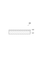
- 1 is a cross-sectional view illustrating one embodiment of a metal sputtering target structure of the present disclosure. 1 is a cross-sectional view showing an example of a film-coated substrate manufactured by a film manufacturing method according to the present disclosure.
- a metal sputtering target containing a metal having a body-centered cubic structure or a face-centered cubic structure When a cross section perpendicular to the sputtering surface of a metal sputtering target is observed using a backscattered electron diffraction method and the crystal orientation is analyzed from the normal direction (ND direction) of the sputtering surface, the ratio of measurement points having an orientation (plane orientation) within 15° from the plane orientation with the highest intensity in the inverse pole figure space obtained from all measurement points to all measurement points is 35 area % or more, and
- This metal sputtering target has a crystal orientation distribution function of the metal sputtering target, in which a crystal coordinate system with the [100] orientation of the crystal as the X-axis, the [010] orientation as the Y-axis, and the [001] orientation as the Z-axis is aligned with the orthogonal sample coordinate systems RD,
- the average value of the orientation density in the range of 0 ⁇ k ⁇ 90 is 1.2 or more in the orientation group of ⁇ 1:k° (0 ⁇ k ⁇ 90), ⁇ :x° (0 ⁇ x ⁇ 90), and ⁇ 2:y° (0 ⁇ y ⁇ 90), and the coefficient of variation of the average value is 0.5 or less for all combinations of (x, y).
- the metal sputtering target of this embodiment is suitable for forming a sputtering film with a uniform thickness by sputtering.
- This embodiment relates to a metal sputtering target containing a metal having a body-centered cubic structure or a face-centered cubic structure (hereinafter also referred to as the "target of this embodiment"), and may be a metal sputtering target containing a metal having a body-centered cubic structure (hereinafter also referred to as a "bcc metal”), or may be a metal sputtering target composed of a bcc metal.
- this embodiment may be a metal sputtering target containing a metal having a face-centered cubic structure (hereinafter also referred to as an "fcc metal”), or may be a metal sputtering target composed of an fcc metal.
- the bcc metal is preferably one or more selected from the group consisting of chromium (Cr), iron (Fe), ruthenium (Ru), niobium (Nb), molybdenum (Mo), tantalum (Ta), vanadium (V) and tungsten (W), more preferably one or more selected from the group consisting of chromium, molybdenum, ruthenium and tungsten, even more preferably one or more selected from the group consisting of chromium, molybdenum and tungsten, and particularly preferably one or more selected from chromium and molybdenum.
- Chromium is preferred from the viewpoint of application of the sputtering film formed by the target of this embodiment as a light-shielding film material in mask blanks, while molybdenum is preferred from the viewpoint of application of the sputtering film formed by the target of this embodiment as a reflective layer material in EUV mask blanks.
- the bcc metal may be an alloy, and examples of alloys constituting the target of this embodiment include alloys containing one or more selected from the group consisting of chromium, iron, ruthenium, niobium, molybdenum, tantalum, vanadium, and tungsten, alloys containing one or more selected from the group consisting of chromium, molybdenum, ruthenium, and tungsten, alloys containing one or more selected from the group consisting of chromium, molybdenum, and tungsten, alloys containing chromium and molybdenum, alloys containing chromium, and chromium-molybdenum alloys.
- the fcc metal is preferably one or more selected from the group consisting of aluminum (Al), copper (Cu) and nickel (Ni), with copper (Cu) being more preferred.
- the fcc metal may be an alloy, and the alloy constituting the target of this embodiment is preferably one or more selected from the group consisting of aluminum (Al), copper (Cu), and nickel (Ni), and examples thereof include an alloy containing one or more selected from the group consisting of aluminum (Al) and copper (Cu), and further an alloy containing one or more selected from the group consisting of copper (Cu) and nickel (Ni).
- the target of this embodiment will be referred to as a "molybdenum sputtering target” if the metal contained in the metal sputtering target is molybdenum, or as a "chromium-molybdenum sputtering target” if the metal contained in the metal sputtering target is a chromium-molybdenum alloy.
- the target of this embodiment may contain an amorphous phase as long as particle generation can be suppressed when using the target of this embodiment.
- the average crystal grain size of the metal contained in the target of this embodiment can be, for example, 200 ⁇ m or less, 150 ⁇ m or less, 100 ⁇ m or less, 80 ⁇ m or less, or 50 ⁇ m or less.
- the average crystal grain size can be, for example, 5 ⁇ m or more, 10 ⁇ m or more, 20 ⁇ m or more, or 30 ⁇ m or more.
- the average crystal grain size can be, for example, 5 ⁇ m or more to 200 ⁇ m or less, 10 ⁇ m or more to 150 ⁇ m or less, or 20 ⁇ m or more to 100 ⁇ m or less.
- the average crystal grain size is the average value of the crystal grain size that can be determined by a method conforming to JIS G 0551:2020 and Annex JC.
- the target of this embodiment preferably has a low content of metal impurities, and for example, the purity of the target of this embodiment is preferably greater than 99.6%, greater than or equal to 99.9%, greater than or equal to 99.99% (4N), or greater than or equal to 99.999% (5N), and may be less than or equal to 100%.
- the purity of the target of this embodiment may be greater than 99.6% and less than or equal to 100%, greater than or equal to 99.9% and less than or equal to 100%, greater than or equal to 99.9% and less than 100%, or greater than or equal to 99.99% and less than 100%.
- the metal impurity content is the content of metal impurities measured by glow discharge mass spectrometry (hereinafter also referred to as "GDMS") according to ASTM F 1593.
- the metal impurities are metals other than bcc metals, and in metal materials made of specific bcc metals, metals other than these.
- metals other than molybdenum are included, and in the case of a chromium-molybdenum sputtering target, metals other than chromium and molybdenum are included.
- the measurement sample may be a prismatic metal material of 10-25 mm x 10-25 mm x 0.5-15 mm.
- the measurement sample may be polished using SiC polishing paper (#800) until the Ra is 1.6 ⁇ m or less, and then pretreated by ultrasonic cleaning in pure water for 10 minutes, dehydrating with alcohol, drying with hot air, and vacuum packaging.
- SiC polishing paper #800
- the oxygen content of the target of this embodiment is preferably 200 ppm by mass or less, and more preferably 150 ppm by mass or less, 30 ppm by mass or less, or 10 ppm by mass or less. This makes it easier to suppress particle generation when the target of this embodiment is used.
- the inclusion of oxygen is permitted as long as it is within a range in which particle generation is suppressed, and examples of the oxygen content include 0 ppm by mass or more, more than 0 ppm by mass, 1 ppm by mass or more, or 3 ppm by mass or more.
- oxygen content examples include 0 ppm by mass or more and 200 ppm by mass or less, more than 0 ppm by mass or more and 150 ppm by mass or less, or 1 ppm by mass or more and 30 ppm by mass or less.
- the oxygen content of the target in this embodiment can be measured using a general oxygen/nitrogen analyzer (e.g., ON736, manufactured by LECO).
- a general oxygen/nitrogen analyzer e.g., ON736, manufactured by LECO.
- the shape of the target in this embodiment is arbitrary, but it is preferable that the shape is suitable for sputtering, for example, one or more selected from the group consisting of plate-like, columnar, and cylindrical.
- the area of the sputtering surface of the target of this embodiment is not particularly limited, but from the viewpoint of increasing the film formation area, it is preferably 200 cm 2 or more, 350 cm 2 or more, or 800 cm 2 or more.
- the area of the sputtering surface may be, for example, 2000 cm 2 or less, 1500 cm 2 or less, or 1200 cm 2 or less.
- the area of the sputtering surface may be 200 cm 2 or more and 2000 cm 2 or less, 350 cm 2 or more and 2000 cm 2 or less, or 350 cm 2 or more and 1500 cm 2 or less.
- ⁇ Orientation rate> when a cross section perpendicular to the sputtering surface of a metal sputtering target is observed using backscattered electron diffraction and the crystal orientation is analyzed from the normal direction (ND direction) of the sputtering surface, the plane orientation (orientation plane orientation) with the highest intensity in the inverse pole figure space obtained from all measurement points on the cross section is specified, and measurement points having an orientation (plane orientation) within 15° from the plane orientation are extracted, and the area ratio to all measurement points is taken as the orientation ratio, and the orientation ratio is 35 area% or more. If the orientation ratio is less than 35 area%, the thickness of the resulting film (sputtering film) becomes non-uniform.
- the orientation rate is preferably 40 area % or more.
- the orientation rate may be 50 area % or more, 60 area % or more, 70 area % or more, or 80 area % or more.
- a high orientation rate is preferable, and examples of the orientation rate include less than 100 area %, 98 area % or less, 95 area % or less, 90 area % or less, 80 area % or less, 70 area % or less, and 60 area % or less.
- the orientation rate may be 35 area % or more and less than 100 area %, 40 area % or more and 98 area % or less, or 50 area % or more and 95 area % or less.
- the orientation rate can be determined from an SEM observation image obtained by scanning electron microscope-electron backscatter diffraction (hereinafter also referred to as "SEM-EBSD") measurement under the following conditions.
- SEM-EBSD scanning electron microscope-electron backscatter diffraction
- the SEM observation image is divided into a 5 ⁇ m ⁇ 5 ⁇ m grid to set the grid points, which are used as measurement points. Then, the orientation planes of all the measurement points are identified, and the area of the orientation planes is measured. Also, the intensity in the inverse pole figure space obtained from each measurement point is obtained, and the plane orientation with the highest intensity is identified.
- the intensity refers to the frequency of occurrence of a specific plane orientation in a state in which the specific plane orientation is completely random, and is a unitless parameter. For example, if the intensity of a specific plane orientation is "5", it means that the specific plane orientation appears five times more frequently than when it is completely random.
- the orientation ratio is calculated from the area ratio of the measurement points having an orientation (plane orientation) within 15° of this plane orientation to all the measurement points.
- SEM observation, identification of the orientation plane, and measurement of its area and the intensity of the inverse pole figure space obtained from each measurement point can be performed using a general SEM-EBSD device (e.g., JSM-IT800, manufactured by JEOL Ltd.) and its associated measurement/analysis program (e.g., AZtec, AZtec Crystal).
- a general SEM-EBSD device e.g., JSM-IT800, manufactured by JEOL Ltd.
- measurement/analysis program e.g., AZtec, AZtec Crystal
- the measurement sample (metal sputtering target) may be mirror-polished using SiC polishing paper and buffing, and then the altered layer of the material may be removed using acid or plasma etching. For example, it may be pretreated by electrolytic etching using a 5% by volume aqueous solution of sulfuric acid.
- ⁇ Crystal orientation distribution function> when a crystal coordinate system in which the [100] orientation of the crystal is the X-axis, the [010] orientation is the Y-axis, and the [001] orientation is the Z-axis, and the crystal coordinate system is rotated around the Z-axis by ⁇ 1 from a state in which it coincides with the orthogonal sample coordinate systems RD, TD, and ND of the sputtering target, and then rotated ⁇ around the X-axis after the rotation, and then rotated ⁇ 2 around the Z-axis after the rotation, the crystal orientation distribution function of the metal sputtering target is expressed using Euler angles ( ⁇ 1, ⁇ , ⁇ 2) that represent crystal orientations.
- the average value of the orientation density in the range of 0 ⁇ k ⁇ 90 (hereinafter also referred to as the “average orientation density”) is 1.2 or more, the variation coefficient of the average orientation density is 0.5 or less for all combinations of (x, y) (combinations of x and y).
- the Euler angles ( ⁇ 1, ⁇ , ⁇ 2) are a set of angles that express the crystal orientation in the sample coordinate system of the metal sputtering target, by rotating the crystal coordinate system around the Z axis by ⁇ 1 from a state in which the crystal coordinate system, with the [100] orientation of the crystal as the X axis, the [010] orientation as the Y axis, and the [001] orientation as the Z axis, coincides with the orthogonal sample coordinate systems RD, TD, and ND of the sputtering target, and then rotating the crystal coordinate system around the Z axis by ⁇ , and then rotating it around the X axis after the rotation, and then rotating it around the Z axis by ⁇ 2.
- the Euler angles ( ⁇ 1, ⁇ , ⁇ 2) are expressed by the Bunge method.
- "ND” is the normal direction of the sputtering surface (the direction perpendicular to the sputtering surface)
- "TD” is the direction perpendicular to "ND” and "RD.”
- "RD” varies depending on the shape of the sputtering surface of the target. For example, if the shape of the sputtering surface is rectangular, “RD” is the longitudinal direction of the rectangle. In this case, “TD” is the direction perpendicular to "ND” and “RD” and is also the width direction. If the sputtering surface is circular in shape, “RD” is the direction along the diameter passing through the center of the circle.
- the in-plane anisotropy of the crystal structure is reduced, which results in improved thickness uniformity of the film during deposition.
- the crystal orientation distribution function is expressed as Euler angles, among all combinations of (x, y) in the orientation group of ⁇ 1:k° (0 ⁇ k ⁇ 90), ⁇ :x° (0 ⁇ x ⁇ 90), and ⁇ 2:y° (0 ⁇ y ⁇ 90)
- the variation coefficient of the average orientation density of any of the combinations of (x, y) in which the average orientation density in the range of 0 ⁇ k ⁇ 90 is 1.2 or more exceeds 0.5, the in-plane anisotropy of the crystal structure becomes large, and the uniformity of the thickness of the obtained film decreases.
- the coefficient of variation of the average orientation density may be 0.4 or less, or 0.3 or less.
- the lower limit of the coefficient of variation of the average orientation density is not particularly limited, but may be 0.01 or more, 0.05 or more, 0.1 or more, or 0.2 or more.
- the coefficient of variation of the average orientation density may be 0.01 or more and 0.5 or less, 0.01 or more and 0.4 or less, or 0.01 or more and 0.3 or less.
- the coefficient of variation of the average orientation density may be 0.01 or more and 0.5 or less, 0.05 or more and 0.5 or less, or 0.1 or more and 0.5 or less.
- the maximum value of the crystal orientation distribution function of the target of this embodiment is preferably 2.0 or more, more preferably 2.5 or more. If the maximum value of the crystal orientation distribution function is 2.0 or more, the anisotropy in the launch angle of the sputtered particles is further reduced, and the film thickness during sputtering is easily controlled.
- As the upper limit of the maximum value of the crystal orientation distribution function for example, 50 or less, 40 or less, or 30 or less can be exemplified.
- the upper limit of the maximum value of the crystal orientation distribution function may be 2.0 or more and 50 or less, 2.0 or more and 40 or less, or 2.5 or more and 30 or less.
- the maximum value of the crystal orientation distribution function may be the maximum value of the orientation density.
- the maximum value of the crystal orientation distribution function in this embodiment is the maximum value of the crystal orientation distribution function (hereinafter also referred to as "ODF") obtained from an SEM observation diagram obtained by a method similar to that for measuring the orientation rate. That is, the SEM observation diagram is analyzed, and the crystal orientations of all measurement points are expressed as Euler angles based on Bunge's notation ( ⁇ 1, ⁇ , ⁇ 2). Next, for the Euler angles, the crystal orientation distribution function (ODF) is calculated using an expansion index of 22 and a Gaussian half-width of 5° as spherical harmonic functions.
- ODF crystal orientation distribution function
- the ODF is calculated at 5° intervals for each, and the maximum value is taken as the maximum value of the crystal orientation distribution function.
- a general analysis program e.g., Aztec Crystal
- the target of the present embodiment can be manufactured by any method, but a preferred method includes a method for manufacturing a target, which includes a pressurizing step of pressurizing an ingot made of a metal having a body-centered cubic structure or a face-centered cubic structure at a pressurizing temperature of 500° C. or higher using a buffer member having a buffer layer to obtain a processed ingot, and a heat treatment step of heat treating the processed ingot at 900° C. or higher.
- an ingot made of a metal having a body-centered cubic structure or a face-centered cubic structure is pressurized at a pressurizing temperature of 500°C or higher and a pressurizing speed of less than 15 mm/s to obtain a processed ingot.
- the ingot to be subjected to the pressurizing process may be an ingot made of a metal having a body-centered cubic structure or a face-centered cubic structure, and is preferably an ingot made of one or more selected from the group consisting of chromium (Cr), iron (Fe), ruthenium (Ru), niobium (Nb), molybdenum (Mo), tantalum (Ta), vanadium (V), tungsten (W), aluminum (Al), copper (Cu), and nickel (Ni), more preferably an ingot made of one or more selected from the group consisting of chromium, molybdenum, ruthenium, and tungsten, even more preferably an ingot made of one or more selected from the group consisting of chromium, molybdenum, and tungsten, even more preferably an ingot made of at least one of chromium and molybdenum, and particularly preferably an ingot made of molybdenum.
- Cr chromium
- the ingot may be an ingot made of an alloy, and examples thereof include an ingot made of an alloy containing one or more selected from the group consisting of chromium, iron, ruthenium, niobium, molybdenum, tantalum, vanadium, tungsten, aluminum, copper, and nickel, an ingot made of an alloy containing one or more selected from the group consisting of chromium, molybdenum, tantalum, vanadium, and tungsten, an ingot made of an alloy containing one or more selected from the group consisting of chromium, molybdenum, and tungsten, an ingot made of an alloy containing chromium and molybdenum, an ingot made of an alloy containing molybdenum, and an ingot made of a chromium-molybdenum alloy.
- the purity of the ingot to be subjected to the pressurizing process may be the same as that of the metal contained in the desired target, and it is preferable that the purity and oxygen content of the ingot to be subjected to the pressurizing process are the same as those of the above-mentioned target.
- the relative density of the ingot to be subjected to the pressing step is preferably 99% or more, or 99.5% or more, which tends to increase the strength of the resulting metal material.
- the relative density of the ingot can be, for example, 100% or less, and the relative density of the ingot can be, for example, 99% to 100% or 99.5% to 100%.
- the average crystal grain size of the ingot subjected to the pressurizing process is arbitrary, but examples of the average crystal grain size are more than 20 ⁇ m or more than 30 ⁇ m.
- examples of the average crystal grain size of the ingot are 2000 ⁇ m or less, 1000 ⁇ m or less, or 400 ⁇ m or less, and examples of the average crystal grain size of the ingot are more than 20 ⁇ m and less than 2000 ⁇ m, more than 20 ⁇ m and less than 1000 ⁇ m, or 30 ⁇ m or more and less than 1000 ⁇ m.
- the maximum value of the orientation distribution function of the ingot subjected to the pressurizing process can be, for example, 5.0 or less.
- the orientation distribution function can be determined in the same manner as the crystal orientation distribution function of the target. This improves the uniformity of the structure after the pressurizing process, and tends to increase the in-plane orientation.
- the maximum value of the orientation distribution function of the ingot can be, for example, 1.2 or more, 2.0 or more, or 2.5 or more, and can be, for example, 1.2 to 5.0, 2.0 to 5.0, or 2.5 to 5.0.
- the ingot is pressurized using a buffer member having a buffer layer in the pressurizing process. That is, in the processing process, the ingot is pressurized while covered with two buffer members.
- one of the two buffer members is a first buffer member made of a buffer layer
- the other buffer member is a second buffer member having a buffer layer and a cylindrical side wall portion provided on the buffer layer.
- the ingot is pressurized while placed in a container formed using the first buffer member and the second buffer member.
- the first buffer member and the second buffer member are preferably welded by electron beam welding or the like in a vacuum atmosphere. At this time, it is preferable that the atmosphere inside the container is a vacuum atmosphere.
- the material of the buffer layer may be any material that can suppress deformation of the surface, etc., where stress is concentrated, by applying pressure together with the ingot during pressure processing.
- the buffer layer has a main body, and the material of the main body of the buffer layer may be any metal whose yield stress is within ⁇ 50% of the yield stress of the ingot.
- the material may be any metal whose yield stress is 200 MPa or more and 600 MPa or less.
- Specific examples include a buffer layer made of chromium-free steel, a buffer layer having a main body made of rolled steel, and a buffer layer having a main body made of carbon steel (SS400) or carbon steel (SN490B).
- the total thickness of the buffer layers of the buffer members arranged on both sides of the ingot is preferably 30% or more of the thickness of the ingot, and more preferably 40% or more.
- the thickness of the buffer layer is not particularly limited, but examples of the thickness include 160% or less, 140% or less, or 100% or less of the thickness of the ingot in order to suppress deformation of the buffer layer itself due to pressure.
- the ratio of the thickness of the buffer layer to the thickness of the ingot is preferably 30% or more and 160% or less, more preferably 30% or more and 140% or less, and even more preferably 40% or more and 100% or less.
- the buffer layer is preferably coated in order to suppress the bonding (thermocompression bonding) between the ingot and the buffer layer during processing. That is, the buffer layer preferably comprises a main body and a coating provided on the surface of the main body.
- the buffer layer having a coating may be one or more selected from the group consisting of powder coating, glass coating, oil-based lubricant coating, and graphite lubricant coating.
- the buffer layer having a graphite lubricant coating is preferable because it has a high effect of preventing thermocompression bonding.
- the coating is preferably heat-treated in a non-oxidizing atmosphere. By performing heat treatment in a non-oxidizing atmosphere, a part of the coating is altered, and the heat resistance of the coating is improved.
- the non-oxidizing atmosphere can be a vacuum atmosphere, an argon atmosphere, a nitrogen atmosphere, or an argon + nitrogen atmosphere, and a vacuum atmosphere is preferable.
- the heat treatment temperature can be 200° C. or more, 225° C. or more, 250° C. or more, or 300° C. or more, and can be 450° C. or less, 400° C. or less, or 350° C. or less.
- the heat treatment temperature can be 200° C.
- the viscosity of the coating liquid containing the graphite lubricant can be, for example, 10 Pa ⁇ s or more or 20 Pa ⁇ s or more.
- the viscosity can be measured using a general cylindrical rotational viscometer (for example, a rotational viscometer VT-06 Viscotester, manufactured by Riontec Co., Ltd.) in accordance with JIS Z 8803.
- examples of the viscosity include 100 Pa ⁇ s or less or 50 Pa ⁇ s or less, and examples of the viscosity include 10 Pa ⁇ s or more and 100 Pa ⁇ s or less, or 20 Pa ⁇ s or more and 50 Pa ⁇ s or less.
- the ingot is pressurized at a pressurizing temperature of 500°C or higher.
- the pressurizing temperature is preferably 600°C or higher or 700°C or higher.
- the pressurizing temperature is preferably 1000°C or lower or 900°C or lower.
- the pressurizing temperature is preferably 500°C or higher and 1000°C or lower, more preferably 600°C or higher and 1000°C or lower, and even more preferably 700°C or higher and 900°C or lower.
- the method of pressure treatment may be any method capable of applying pressure to the ingot, and may be, for example, one or more methods selected from the group consisting of forging, drawing, extrusion, and rolling.
- the pressurization process it is preferable to pressurize the ingot so that the ratio of the ingot's length in the X direction to the ingot's length in the Z direction (hereinafter also referred to as the "size ratio") is 0.5 or more or 0.6 or more, where the direction in which pressure is applied to the ingot is the Z direction and the direction perpendicular to the Z direction is the X direction.
- the size ratio is 8 or less or 4 or less further suppresses the generation of cracks due to deformation. It is more preferable that the size ratio of the ingot before the pressurization process is 0.5 to 8 or 0.6 to 4.
- both the size ratio calculated from the ratio of the ingot's maximum length in the X direction to the ingot's length in the Z direction and the size ratio calculated from the ratio of the ingot's minimum length in the X direction to the ingot's length in the Z direction satisfy the above-mentioned values.
- Pressure treatment in the pressurizing step is preferably performed two or more times, and more preferably three or more times.
- pressure treatment By performing pressure treatment under the above conditions multiple times, it is possible to introduce strain into the target without causing defects such as ingot cracking. As a result, a target with a high orientation area ratio (orientation rate) is more likely to be obtained. Since the surface and interior of the obtained target tend to have a more uniform structure, it is preferable that pressure treatment be performed 20 times or less.
- Pressure treatment is preferably performed 2 to 20 times, and more preferably 3 to 20 times.
- the temperature of the ingot may decrease before and after the pressure treatment. If the pressure treatment is performed multiple times in the pressure process, it is preferable to heat the ingot to the pressure temperature before each pressure treatment before performing the pressure treatment in order to prevent a decrease in the ingot temperature.
- the total rolling reduction of the processed ingot after the pressurizing step is preferably 50% or more or 60% or more.
- the upper limit of the total rolling reduction can be, for example, 95% or less or 90% or less.
- the total rolling reduction is preferably 50% or more and 95% or less, more preferably 60% or more and 95% or less, and even more preferably 60% or more and 90% or less.
- the total rolling reduction can be calculated from the following formula.
- Total rolling reduction rate [%] (1 - thickness of pressed ingot / thickness of ingot before processing) x 100
- the heat treatment step it is preferable to heat treat the processed ingot at a heat treatment temperature of 900°C or higher. If the heat treatment temperature is less than 900°C, it is difficult to align the orientation.
- the heat treatment temperature is preferably 1500°C or higher.
- the heat treatment temperature does not need to be higher than necessary, and may be 2200°C or lower or 2000°C or lower.
- the heat treatment temperature is preferably 900°C or higher and 2200°C or lower, and more preferably 1500°C or higher and 2000°C or lower.
- the heat treatment atmosphere is arbitrary and may be an air atmosphere, an inert atmosphere, a reducing atmosphere, or a vacuum atmosphere, and is preferably an inert atmosphere, a reducing atmosphere, or a vacuum atmosphere. It is more preferable that the heat treatment atmosphere is a reducing atmosphere or a vacuum atmosphere.
- the heat treatment time can be adjusted appropriately depending on the size of the processed ingot to be subjected to the heat treatment process and the performance of the heat treatment furnace, and can be, for example, from 1 hour to 5 hours.
- the manufacturing method of this embodiment may include a processing step of processing the processed ingot prior to the heat treatment step.
- the processing method is arbitrary, and may be, for example, cutting.
- the manufacturing method of this embodiment may further include a surface treatment step of surface-treating the metal material after the heat treatment step.
- a metal sputtering target structure (hereinafter also referred to as a "target structure”) 100 of this embodiment includes a target 10 and a backing plate 20.
- the target 10 is formed from the target described above.
- This target structure 100 is also suitable for forming a film with a uniform thickness by sputtering.
- the backing plate 20 may be made of any material that can conduct electricity and dissipate heat during sputtering, and examples of such materials include backing plates made of one or more materials selected from the group consisting of copper (Cu), aluminum (Al), titanium (Ti), and stainless steel.
- the backing plate 20 may be directly bonded to the target 10, or may be bonded via a bonding material 30 as shown in FIG. 1.
- the bonding material 30 may be any known material, such as indium (In).
- the target structure 100 of this embodiment can be manufactured by a manufacturing method that includes a bonding process for bonding the target 10 and the backing plate 20.
- the bonding method in the bonding process may be any method capable of bonding the backing plate 20 and the target 10, and may be, for example, one or more methods selected from the group consisting of diffusion bonding, solder bonding, and friction stir bonding.
- the film manufacturing method (film formation method) of the present embodiment is a method using the target or target structure of the present embodiment. That is, the target or target structure of the present embodiment can be used in a film manufacturing method using the target or target structure.
- the film 202 is formed by a sputtering method. That is, the film manufacturing method of the present embodiment is a method of manufacturing a film-coated substrate 200 by sputtering the target 10 of the present embodiment to manufacture a film 202 on a substrate 201 (see FIG. 2).
- the film manufacturing method of the present embodiment provides a film 202.
- the film 202 may be a thin film or a sputtered film (sputtering film).
- the substrate 201 is not particularly limited, but examples thereof include a silicon substrate, a glass substrate, and a quartz substrate.
- the temperature of the substrate 201 (film formation temperature) is not particularly limited, but may be, for example, room temperature (25° C.).
- the process gas used during film formation is not particularly limited as long as it is a gas type that causes sputtering by discharge, and may be, for example, argon.
- the gas pressure during film formation is not particularly limited, but may be, for example, 0.1 Pa or more and 1 Pa or less.
- the acceleration voltage during film formation is not particularly limited, but may be, for example, 1 kV or more and 3 kV or less.
- the film formation time is not particularly limited, but may be, for example, 10 minutes or more and 60 minutes or less.
- the sputtering can be carried out using a general sputtering device.
- the film may be produced (formed) by any method, but may be produced, for example, by the following method.
- Ultimate vacuum 1 ⁇ 10 -4 Pa
- Process gas Argon (Ar)
- Gas partial pressure 0.5 Pa
- Film forming temperature room temperature (25°C)
- Substrate Si substrate Acceleration voltage: 2 kV
- the orientation rate of the plane direction was determined as follows. First, a SEM-EBSD apparatus (apparatus name: JSM-IT800, manufactured by JEOL Ltd.), a measurement program (software name: AZtec) and an analysis program (software name: AZtec Crystal) were used to obtain SEM observation diagrams by SEM-EBSD measurement under the following conditions for the metal sputtering targets obtained in the following examples and comparative examples. Observation magnification: 10x Acceleration voltage: 20 kV Irradiation current: 100 ⁇ A Working distance: 10mm Step width: 5 ⁇ m
- the SEM observation image was then divided into a 5 ⁇ m x 5 ⁇ m grid to create grid points, and each grid point was used as a measurement point.
- the orientation plane and area of all measurement points were measured, and the intensity in the inverse pole figure space obtained from each measurement point was determined, and the plane orientation (orientation plane orientation) with the highest intensity was identified.
- Measurement points with an orientation (plane orientation) within 15° of the plane orientation were selected, and the orientation rate [area %] was calculated from the area ratio to all measurement points.
- the above SEM-EBSD measurements were performed on metal sputtering targets obtained as follows. That is, first, the radius of the circular sputtering surface (sputter surface) of the disk-shaped target was taken as R, and a width of 3 mm was taken radially inward from a position 0.7R away from the center of the circle, and a cross-sectional portion of width 3 mm x total target thickness t (mm) was observed in a direction perpendicular to the sputter surface.
- the cross-sectional portion (the portion that would become the measurement surface) was mirror-polished using SiC polishing paper and buff polishing, and then pretreated by electrolytic etching with a 5% by volume aqueous sulfuric acid solution to obtain a measurement area. SEM-EBSD measurements were then performed on the measurement area.
- Crystal orientation distribution function (Crystal orientation distribution function) Using the SEM observation diagram obtained in the measurement of the orientation rate, the measurement results were analyzed using an analysis program (Aztec Crystal) at all measurement points of the SEM observation diagram, and the crystal orientation at each measurement point was obtained and expressed as Euler angles. The Euler angles were expressed using Bunge's notation ( ⁇ 1, ⁇ , ⁇ 2). Based on the Euler angles obtained at each measurement point, an analysis program (Aztec Crystal) was used to calculate a crystal orientation distribution function (ODF) using an expansion index of 22 and a Gaussian half-width of 5° as a spherical harmonic function.
- ODF crystal orientation distribution function
- x, y and k were each output at 5° intervals.
- the oxygen content was measured using an oxygen/nitrogen analyzer (device name: ON736, manufactured by LECO). A metal material cut into a prismatic shape of 4 mm x 4 mm x 5 mm was used as a measurement sample.
- Example 1 210 kg of molybdenum powder (purity 5N) was placed in a soft iron can measuring 350 mm ⁇ 350 mm ⁇ 350 mm and subjected to HIP treatment under the following conditions.
- HIP treatment atmosphere Argon gas atmosphere
- HIP treatment temperature 1250°C
- HIP processing pressure 150 MPa
- HIP processing time 5 hours
- the resulting HIP body was ground and cut to adjust the shape, obtaining a disk-shaped ingot with a diameter of 180 mm and a thickness of 50 mm (dimension ratio 3.6), which was used as the molybdenum material for this example.
- the average crystal grain size of the ingot was 22.7 ⁇ m, and the maximum ODF was 3.7.
- a first buffer member and a second buffer member were prepared as buffer members for the ingot.
- an oil-based lubricant containing 30% or more graphite manufactured by Nippon Graphite Industries Co., Ltd., product name: Rolling Oil, viscosity: 24 Pa ⁇ s
- a coating liquid with a viscosity of 20 Pa ⁇ s was applied to the surface of a disk-shaped member made of SS400 (thickness 25 mm, diameter 240 mm), and heat treatment was performed for 30 minutes in a vacuum atmosphere at a heat treatment temperature of 300°C to obtain a buffer layer.
- a cylindrical box-shaped buffer member was used, which was obtained by applying the above coating liquid to the surface of the buffer layer and the inner surface of the side wall of a cylindrical member consisting of a disk-shaped buffer layer made of SS400 (thickness 25 mm, diameter 240 mm) and a cylindrical side wall portion with a height of 55 mm extending from the peripheral portion of the surface of the buffer layer, and heat treatment was performed for 30 minutes in a vacuum atmosphere at a heat treatment temperature of 300°C.
- the ingot was then placed on the surface of the buffer layer of the second buffer member, and the first buffer member was placed on the side wall of the second buffer member so as to cover the ingot to form a container.
- the inside of the container was placed in a vacuum atmosphere, and the first buffer member and the second buffer member were welded together by electron beam welding to perform sealing.
- the thickness of the buffer layers placed on both sides of the ingot was 100% of the thickness of the ingot.
- the ingot placed in the cylindrical box-shaped buffer layer was heated to 800°C, and then pressure treatment was performed on the heated ingot in the thickness direction of the ingot at a pressure speed of 7 mm/sec.
- pressure treatment was performed so that the length of the ingot in the direction in which pressure was applied (Z direction) was 50 mm, and the length in the direction perpendicular to the Z direction (X direction) was 180 mm.
- This pressure treatment was repeated 16 times to obtain an ingot (processed ingot) with a diameter of 330 mm and a thickness of 15 mm (total reduction rate of 85%).
- the temperature of the ingot after each pressure treatment was 450°C or lower, the ingot was heated to 800°C and then pressure treatment was performed.
- the processed ingot was treated in an argon atmosphere at 1500°C for 3 hours to obtain a disk-shaped molybdenum sputtering target with a diameter of 330 mm and a thickness of 15 mm, which was used as the molybdenum sputtering target of this example.
- the orientation plane direction, orientation rate, and maximum ODF of this molybdenum sputtering target were as shown in Table 1.
- Example 2 A molybdenum sputtering target was produced in the same manner as in Example 1, except that a molybdenum ingot was obtained in the same manner as in Example 1, the obtained ingot was ground and cut to adjust the shape to a diameter of 180 mm and a thickness of 55 mm (dimension ratio 3.3), the ingot was pressurized with the ratio of the thickness of the buffer layer to the thickness of the ingot being 91%, and the total rolling reduction was set to 70% so that the orientation plane orientation, orientation rate, and maximum value of ODF were as shown in Table 1.
- Example 3 Chromium powder (purity 4N) was placed in a soft iron can of 350 mm ⁇ 350 mm ⁇ 350 mm and subjected to HIP treatment under the following conditions.
- HIP treatment atmosphere Argon gas atmosphere
- HIP treatment temperature 1150°C
- HIP processing pressure 100 MPa
- HIP processing time 2 hours
- the resulting HIP body was ground and cut to adjust the shape, yielding a disk-shaped chromium ingot with a diameter of 180 mm and a thickness of 60 mm.
- the average crystal grain size of the ingot was 116.4 ⁇ m, and the maximum ODF was 1.3.
- the pressurized ingot was obtained in the same manner as in Example 1, except that the obtained ingot was ground and cut to adjust the shape to 90 mm in diameter and 60 mm in thickness (dimension ratio 1.5), the thickness of the buffer layer was set to 83% of the thickness of the ingot, and the pressurization was performed 8 times.
- the processed ingot was treated in an argon atmosphere at 1600°C for 1 hour, and then ground and cut to adjust the shape to obtain a chromium sputtering target, which was used as the chromium sputtering target of this example.
- the orientation plane direction, orientation rate, and maximum ODF of this chromium sputtering target were as shown in Table 1.
- Example 4 A chromium ingot was obtained in the same manner as in Example 3, and the obtained ingot was ground and cut to adjust the shape to a diameter of 60 mm and a thickness of 90 mm (dimension ratio 0.67).
- a pressurized ingot was obtained in the same manner as in Example 1, except that SN490B was used instead of SS400 as the disk-shaped member, the ratio of the thickness of the buffer layer to the thickness of the ingot was 56%, the temperature of the ingot was 1000° C., the pressure treatment was performed 8 times, and the total rolling reduction was 70%, so that the maximum values of the orientation plane orientation, orientation rate, and ODF were as shown in Table 1.
- the processed ingot was treated in air at 1000°C for 1 hour to produce a chromium sputtering target.
- Example 5 A chromium ingot was obtained in the same manner as in Example 3, and the obtained ingot was ground and cut to adjust the shape to a diameter of 120 mm and a thickness of 40 mm (dimension ratio 3.0).
- a pressurized ingot was obtained in the same manner as in Example 1, except that the heat treatment temperature of the buffer member was 400° C., the ratio of the thickness of the buffer layer to the thickness of the ingot was 125%, and the total rolling reduction was 70%, so that the orientation plane orientation, orientation rate, and maximum value of ODF were as shown in Table 1.
- the obtained processed ingot was treated in an air atmosphere at 1000° C. for 1 hour to prepare a chromium sputtering target.
- Example 6 The obtained HIP body was ground and cut to adjust the shape to 180 mm in diameter and 55 mm in thickness (dimension ratio 3.3), the heat treatment temperature of the buffer member was set to 250° C., the ratio of the thickness of the buffer layer to the thickness of the ingot was set to 91%, and the total rolling reduction was set to 70%, so that the orientation plane orientation, orientation rate, and maximum value of ODF were as shown in Table 1.
- a molybdenum sputtering target was produced in the same manner as in Example 1, except for the following.
- Example 7 The obtained HIP body was ground and cut to adjust the shape to 180 mm in diameter and 55 mm in thickness (dimension ratio 3.3), a buffer layer with a thickness of SS400 of 10 mm instead of 25 mm was used, the ratio of the buffer layer thickness to the ingot thickness was 36%, and the total rolling reduction was 70% so that the orientation plane orientation, orientation rate, and maximum value of ODF were as shown in Table 1.
- a molybdenum sputtering target was produced in the same manner as in Example 1, except for the following.
- the resulting HIP body was ground and cut to adjust the shape, yielding a disk-shaped ingot with a diameter of 180 mm and a thickness of 50 mm.
- a first buffer member and a second buffer member were prepared as the buffer layer of the ingot.
- an oil-based lubricant containing 30% or more of graphite manufactured by Nippon Graphite Industries Co., Ltd., product name: Rolling Oil, viscosity: 24 Pa ⁇ s
- a coating liquid with a viscosity of 20 Pa ⁇ s was applied to the surface of a disk-shaped member (thickness 25 mm, diameter 240 mm) made of SS400, and a heat treatment was performed for 30 minutes at a heat treatment temperature of 300 ° C. in the atmosphere to obtain a buffer layer.
- a cylindrical box-shaped buffer member was used, which was obtained by applying the above coating liquid to the surface of the buffer layer and the inner surface of the side wall of a cylindrical member consisting of a disk-shaped buffer layer (thickness 25 mm, diameter 240 mm) made of SS400 and a cylindrical side wall portion with a height of 55 mm extending from the peripheral portion of the surface of the buffer layer, and performing a heat treatment for 30 minutes at a heat treatment temperature of 300 ° C. in the atmosphere.
- the ingot was placed on the surface of the buffer layer of the second buffer member, and the first buffer member was placed on the side wall of the second buffer member so as to cover the ingot to form a container.
- the inside of the container was made into a vacuum atmosphere, and the first buffer member and the second buffer member were welded together by electron beam welding to perform sealing.
- the ratio of the thickness of the buffer layer to the thickness of the ingot was 100%.
- the obtained ingot was heated to 800°C, and then pressure treatment was performed on the heated ingot in the thickness direction at a pressure speed of 7 mm/sec.
- the pressure treatment was repeated 16 times to obtain an ingot (processed ingot) with a diameter of 330 mm and a thickness of 15 mm (total rolling reduction rate of 70%).
- the temperature of the ingot after each pressure treatment was 450°C or less, the ingot was heated to 800°C and then pressure treatment was performed.
- the processed ingot was treated in an argon atmosphere at 1500°C for 3 hours to obtain a disk-shaped molybdenum sputtering target with a diameter of 330 mm and a thickness of 15 mm, which was used as the molybdenum sputtering target of this comparative example.
- the orientation plane direction, orientation rate, and maximum ODF of this molybdenum sputtering target were as shown in Table 1.
- Example 2 A chromium ingot was obtained in the same manner as in Example 3, and the shape of the chromium ingot was adjusted by grinding and cutting to a diameter of 200 mm and a thickness of 50 mm (a dimension ratio of 4.0).
- a buffer member having a thickness of SS400 of 7 mm instead of 25 mm was used.
- the ratio of the thickness of the buffer layer to the thickness of the ingot was set to 28%.
- the total rolling reduction was set to 80%, so that the maximum values of the orientation plane orientation, the orientation rate, and the ODF were as shown in Table 1.
- a pressed ingot was obtained in the same manner as in Example 1.
- the obtained processed ingot was treated in an air atmosphere at 1000° C. for 1 hour to prepare a chromium sputtering target.
- Example 3 A chromium ingot was obtained in the same manner as in Example 3, and the shape of the chromium ingot was adjusted by grinding and cutting to a diameter of 90 mm and a thickness of 30 mm (a dimension ratio of 3.0).
- a pressurized ingot was obtained in the same manner as in Example 1, except that a buffer member was not used, the pressurization treatment was repeated eight times, the ratio of the thickness of the buffer layer to the thickness of the ingot was set to 167%, and the total rolling reduction was set to 70%, so that the maximum values of the orientation plane orientation, the orientation rate, and the ODF were as shown in Table 1.
- the obtained processed ingot was treated in an air atmosphere at 1000° C. for 1 hour to prepare a chromium sputtering target.
- Example 4 A chromium ingot was obtained in the same manner as in Example 3, and the chromium ingot was ground and cut to adjust the shape to a diameter of 80 mm and a thickness of 40 mm (a dimension ratio of 2.0).
- a buffer member made of cast iron (FC200, thickness 25 mm) instead of SS400 was used.
- the ratio of the thickness of the buffer layer to the thickness of the ingot was 167%.
- the total rolling reduction was 80%, so that the maximum values of the orientation plane orientation, the orientation rate, and the ODF were as shown in Table 1.
- a pressed ingot was obtained in the same manner as in Example 1.
- the obtained processed ingot was treated in an air atmosphere at 1000° C. for 1 hour to prepare a chromium sputtering target.
- Example 5 A chromium ingot was obtained in the same manner as in Example 3, and the shape of the chromium ingot was adjusted by grinding and cutting to a diameter of 75 mm and a thickness of 25 mm (a dimension ratio of 3.0).
- a BN-based release agent manufactured by Advanced Technical Products, Inc., model number: ATP-R33
- the ratio of the thickness of the buffer layer to the thickness of the ingot was set to 200%.
- the total rolling reduction was set to 65%, so that the maximum values of the orientation plane orientation, the orientation rate, and the ODF were as shown in Table 1.
- a pressed ingot was obtained in the same manner as in Example 1. The obtained processed ingot was treated in an air atmosphere at 1000° C. for 1 hour to prepare a chromium sputtering target.
- Example 6 A chromium ingot was obtained in the same manner as in Example 3, and the chromium ingot was ground and cut to adjust the shape to a diameter of 70 mm and a thickness of 30 mm (a dimension ratio of 2.3).
- the heat treatment temperature of the buffer member was set to 500° C.
- the ratio of the thickness of the buffer layer to the thickness of the ingot was set to 167%
- the total rolling reduction was set to 70%, so that the orientation plane orientation, the orientation rate, and the maximum value of the ODF were as shown in Table 1.
- a pressed ingot was obtained in the same manner as in Example 1, except for the above.
- the obtained processed ingot was treated in an air atmosphere at 1000° C. for 1 hour to prepare a chromium sputtering target.
- a pressurized ingot was obtained in the same manner as in Example 1, except that the ingot was pressurized and the total rolling reduction rate was set to 70% so that the orientation plane orientation, orientation rate, and maximum value of ODF were as shown in Table 1.
- the obtained processed ingot was treated in an argon atmosphere at 1500° C. for 3 hours to prepare a molybdenum sputtering target.
- the (x, y) values with an average orientation density of 1.2 or more were 110 in Example 1, 35 in Example 2, 21 in Example 3, 157 in Example 4, 88 in Example 5, 38 in Example 6, and 36 in Example 7, and it was confirmed that the coefficients of variation for all of them were 0.5 or less.
- the coefficients of variation for (x, y) with an average orientation density of 1.2 or more sometimes exceeded 0.5.
- Tables 2A and 2B show the average orientation density of Example 1, and Tables 3A and 3B show the variation coefficients of (x, y) when the average orientation density of Example 1 is 1.2 or more.
- Tables 4A and 4B show the average orientation density of Example 2, and Tables 5A and 5B show the variation coefficients of (x, y) when the average orientation density of Example 2 is 1.2 or more.
- Tables 6A and 6B show the average orientation density of Example 3 and Tables 7A and 7B show the variation coefficients of (x, y) when the average orientation density of Example 3 is 1.2 or more.
- Tables 8A and 8B show the average orientation density of Example 4, and Tables 9A and 9B show the variation coefficients of (x, y) when the average orientation density of Example 4 is 1.2 or more.
- Tables 10A and 10B show the average orientation density of Example 5, and Tables 11A and 11B show the variation coefficients of (x, y) when the average orientation density of Example 5 is 1.2 or more.
- Tables 12A and 12B show the average orientation density of Example 6, and Tables 13A and 13B show the variation coefficients of (x, y) when the average orientation density of Example 6 is 1.2 or more.
- Tables 14A and 14B show the average orientation density of Example 7, and Tables 15A and 15B show the variation coefficients of (x, y) when the average orientation density of Example 7 is 1.2 or more.
- Tables 16A and 16B show the average orientation density of Comparative Example 1
- Tables 17A and 17B show the variation coefficients of (x, y) when the average orientation density of Comparative Example 1 is 1.2 or more.
- Tables 18A and 18B show the average orientation density of Comparative Example 2
- Tables 19A and 19B show the variation coefficients of (x, y) when the average orientation density of Comparative Example 2 is 1.2 or more.
- Tables 20A and 20B show the average orientation density of Comparative Example 3, and Tables 21A and 21B show the variation coefficients of (x, y) when the average orientation density of Comparative Example 3 is 1.2 or more.
- Tables 22A and 22B show the average orientation density of Comparative Example 4, and Tables 23A and 23B show the variation coefficients of (x, y) when the average orientation density of Comparative Example 4 is 1.2 or more.
- Tables 24A and 24B show the average orientation density of Comparative Example 5, and Tables 25A and 25B show the variation coefficients of (x, y) when the average orientation density of Comparative Example 5 is 1.2 or more.
- Tables 26A and 26B show the average orientation density of Comparative Example 6, and Tables 27A and 27B show the variation coefficients of (x, y) when the average orientation density of Comparative Example 6 is 1.2 or more.
- Tables 28A and 28B show the average orientation density of Comparative Example 7, and Tables 29A and 29B show the variation coefficients of (x, y) when the average orientation density of Comparative Example 7 is 1.2 or more.
- Tables 30A and 30B show the average orientation density of Comparative Example 8, and Tables 31A and 31B show the variation coefficients of (x, y) when the average orientation density of Comparative Example 8 is 1.2 or more.
- Tables 3A and 3B Tables 5A and 5B, Tables 7A and 7B, Tables 9A and 9B, Tables 11A and 11B, Tables 13A and 13B, Tables 15A and 15B, Tables 17A and 17B, Tables 19A and 19B, Tables 21A and 21B, Tables 23A and 23B, Tables 25A and 25B, Tables 27A and 27B, Tables 29A and 29B, and Tables 31A and 31B, "Not applicable" indicates a combination of (x, y) for which the average orientation density is less than 1.2.
- the deposition rate was calculated by the following formula.
- Film formation rate [nm/min] average film thickness [nm] / film formation time [min]
- the average film thickness is the average value of the film thicknesses at the measurement points.
- the film thickness was measured at a total of 64 points on the glass substrate after film formation (glass substrate having a sputtered film): (1) the center, (2) six equally spaced points on the circumference of a concentric circle having a diameter equivalent to 1 ⁇ 4 of the diameter of the substrate, (3) 13 equally spaced points on the circumference of a concentric circle having a diameter equivalent to 1 ⁇ 4 of the diameter of the substrate, (4) 19 equally spaced points on the circumference of a concentric circle having a diameter equivalent to 3 ⁇ 4 of the diameter of the substrate, and (5) 25 equally spaced points on the circumference of a concentric circle having a diameter equivalent to 3 ⁇ 4 of the diameter of the substrate.
Landscapes
- Chemical & Material Sciences (AREA)
- Chemical Kinetics & Catalysis (AREA)
- Engineering & Computer Science (AREA)
- Materials Engineering (AREA)
- Mechanical Engineering (AREA)
- Metallurgy (AREA)
- Organic Chemistry (AREA)
- Physical Vapour Deposition (AREA)
Priority Applications (2)
| Application Number | Priority Date | Filing Date | Title |
|---|---|---|---|
| JP2025540718A JPWO2025037642A1 (https=) | 2023-08-17 | 2024-08-15 | |
| KR1020267004277A KR20260043103A (ko) | 2023-08-17 | 2024-08-15 | 금속 스퍼터링 타깃, 금속 스퍼터링 타깃 구조체 및 이것들을 사용한 막의 제조 방법, 그리고 금속 스퍼터링 타깃의 제조 방법 |
Applications Claiming Priority (4)
| Application Number | Priority Date | Filing Date | Title |
|---|---|---|---|
| JP2023-133069 | 2023-08-17 | ||
| JP2023133069 | 2023-08-17 | ||
| JP2023-202660 | 2023-11-30 | ||
| JP2023202660 | 2023-11-30 |
Publications (1)
| Publication Number | Publication Date |
|---|---|
| WO2025037642A1 true WO2025037642A1 (ja) | 2025-02-20 |
Family
ID=94632577
Family Applications (1)
| Application Number | Title | Priority Date | Filing Date |
|---|---|---|---|
| PCT/JP2024/029116 Pending WO2025037642A1 (ja) | 2023-08-17 | 2024-08-15 | 金属スパッタリングターゲット、金属スパッタリングターゲット構造体及びこれらを用いた膜の製造方法、並びに金属スパッタリングターゲットの製造方法 |
Country Status (4)
| Country | Link |
|---|---|
| JP (1) | JPWO2025037642A1 (https=) |
| KR (1) | KR20260043103A (https=) |
| TW (1) | TW202509256A (https=) |
| WO (1) | WO2025037642A1 (https=) |
Citations (7)
| Publication number | Priority date | Publication date | Assignee | Title |
|---|---|---|---|---|
| US20050155677A1 (en) * | 2004-01-08 | 2005-07-21 | Wickersham Charles E.Jr. | Tantalum and other metals with (110) orientation |
| WO2009107763A1 (ja) * | 2008-02-29 | 2009-09-03 | 新日鉄マテリアルズ株式会社 | 金属系スパッタリングターゲット材 |
| WO2011052171A1 (ja) * | 2009-10-26 | 2011-05-05 | 株式会社アルバック | チタン含有スパッタリングターゲットの製造方法 |
| JP2012507626A (ja) | 2008-11-03 | 2012-03-29 | トーソー エスエムディー,インク. | スパッターターゲットを製造する方法と当該方法によって製造されるスパッターターゲット |
| JP2014129599A (ja) | 2007-05-04 | 2014-07-10 | Hc Starck Inc | 均一ランダム結晶配向の、微細粒でバンディングのない耐火金属スパッタリングターゲット、そのような膜の製造方法、およびそれから作製される薄膜ベースのデバイスおよび製品 |
| CN111286703A (zh) * | 2020-03-31 | 2020-06-16 | 贵研铂业股份有限公司 | 一种镍铂合金溅射靶材及其制备方法 |
| JP2023133069A (ja) | 2022-03-11 | 2023-09-22 | 株式会社リコー | 液体吐出装置、および液体吐出方法 |
-
2024
- 2024-08-15 KR KR1020267004277A patent/KR20260043103A/ko active Pending
- 2024-08-15 JP JP2025540718A patent/JPWO2025037642A1/ja active Pending
- 2024-08-15 WO PCT/JP2024/029116 patent/WO2025037642A1/ja active Pending
- 2024-08-15 TW TW113130751A patent/TW202509256A/zh unknown
Patent Citations (7)
| Publication number | Priority date | Publication date | Assignee | Title |
|---|---|---|---|---|
| US20050155677A1 (en) * | 2004-01-08 | 2005-07-21 | Wickersham Charles E.Jr. | Tantalum and other metals with (110) orientation |
| JP2014129599A (ja) | 2007-05-04 | 2014-07-10 | Hc Starck Inc | 均一ランダム結晶配向の、微細粒でバンディングのない耐火金属スパッタリングターゲット、そのような膜の製造方法、およびそれから作製される薄膜ベースのデバイスおよび製品 |
| WO2009107763A1 (ja) * | 2008-02-29 | 2009-09-03 | 新日鉄マテリアルズ株式会社 | 金属系スパッタリングターゲット材 |
| JP2012507626A (ja) | 2008-11-03 | 2012-03-29 | トーソー エスエムディー,インク. | スパッターターゲットを製造する方法と当該方法によって製造されるスパッターターゲット |
| WO2011052171A1 (ja) * | 2009-10-26 | 2011-05-05 | 株式会社アルバック | チタン含有スパッタリングターゲットの製造方法 |
| CN111286703A (zh) * | 2020-03-31 | 2020-06-16 | 贵研铂业股份有限公司 | 一种镍铂合金溅射靶材及其制备方法 |
| JP2023133069A (ja) | 2022-03-11 | 2023-09-22 | 株式会社リコー | 液体吐出装置、および液体吐出方法 |
Non-Patent Citations (2)
| Title |
|---|
| F. BOUCHARD ET AL., J. VAC. SCI. TECHNOL. A, vol. 11, 1993, pages 2765 |
| GOTTFRIED K. WEHNER, PHYS. REV., vol. 102, 1956, pages 690 |
Also Published As
| Publication number | Publication date |
|---|---|
| KR20260043103A (ko) | 2026-03-31 |
| TW202509256A (zh) | 2025-03-01 |
| JPWO2025037642A1 (https=) | 2025-02-20 |
Similar Documents
| Publication | Publication Date | Title |
|---|---|---|
| CN101155650B (zh) | 溅射靶 | |
| CN103797153B (zh) | Mo-W靶材及其制造方法 | |
| CN101278071B (zh) | 溅射靶 | |
| JP7108606B2 (ja) | スパッタリングターゲット | |
| WO2025037642A1 (ja) | 金属スパッタリングターゲット、金属スパッタリングターゲット構造体及びこれらを用いた膜の製造方法、並びに金属スパッタリングターゲットの製造方法 | |
| JP6602550B2 (ja) | スパッタリングターゲット用材料 | |
| EP3467141B1 (en) | Gold sputtering target | |
| CN121986184A (en) | Metal sputtering target, metal sputtering target structure, method for producing film using same, and method for producing metal sputtering target | |
| CN109154074B (zh) | 钽溅射靶 | |
| US20250354251A1 (en) | Metallic sputtering target, production method therefor, and metallic material and production method therefor | |
| JP6871301B2 (ja) | スパッタリングターゲット、窒化チタン膜の製造方法、および半導体素子の製造方法 | |
| US12020916B2 (en) | Niobium sputtering target | |
| JP2001303243A (ja) | スパッタリングターゲットとその製造方法、および電子部品 | |
| CN118591653A (zh) | 金属溅射靶及其制造方法、以及金属材料及其制造方法 | |
| TW202319555A (zh) | 濺鍍靶材、其製造方法、及經使用濺鍍靶材的濺鍍膜的製造方法 | |
| EP4570943A1 (en) | Molybdenum sputtering target, method for producing same, and method for producing sputtering film using molybdenum sputtering target | |
| KR20230133222A (ko) | 크롬 소결체 및 그 제조 방법, 스퍼터링 타깃 및 크롬막 부착 기판의 제조 방법 | |
| JP2002038260A (ja) | スパッタリングターゲットおよびその製造方法 |
Legal Events
| Date | Code | Title | Description |
|---|---|---|---|
| 121 | Ep: the epo has been informed by wipo that ep was designated in this application |
Ref document number: 24854230 Country of ref document: EP Kind code of ref document: A1 |
|
| ENP | Entry into the national phase |
Ref document number: 2025540718 Country of ref document: JP Kind code of ref document: A |
|
| WWE | Wipo information: entry into national phase |
Ref document number: 2025540718 Country of ref document: JP |
|
| ENP | Entry into the national phase |
Ref document number: 1020267004277 Country of ref document: KR Free format text: ST27 STATUS EVENT CODE: A-0-1-A10-A15-NAP-PA0105 (AS PROVIDED BY THE NATIONAL OFFICE) |
|
| WWE | Wipo information: entry into national phase |
Ref document number: 2024854230 Country of ref document: EP |
|
| NENP | Non-entry into the national phase |
Ref country code: DE |
|
| WWE | Wipo information: entry into national phase |
Ref document number: 11202600893X Country of ref document: SG |
|
| WWP | Wipo information: published in national office |
Ref document number: 11202600893X Country of ref document: SG |