WO2025022820A1 - 樹脂積層基板及び樹脂積層基板の製造方法 - Google Patents
樹脂積層基板及び樹脂積層基板の製造方法 Download PDFInfo
- Publication number
- WO2025022820A1 WO2025022820A1 PCT/JP2024/020154 JP2024020154W WO2025022820A1 WO 2025022820 A1 WO2025022820 A1 WO 2025022820A1 JP 2024020154 W JP2024020154 W JP 2024020154W WO 2025022820 A1 WO2025022820 A1 WO 2025022820A1
- Authority
- WO
- WIPO (PCT)
- Prior art keywords
- resin
- resin layer
- layer
- conductor
- main surface
- Prior art date
- Legal status (The legal status is an assumption and is not a legal conclusion. Google has not performed a legal analysis and makes no representation as to the accuracy of the status listed.)
- Pending
Links
Images


Classifications
-
- H—ELECTRICITY
- H05—ELECTRIC TECHNIQUES NOT OTHERWISE PROVIDED FOR
- H05K—PRINTED CIRCUITS; CASINGS OR CONSTRUCTIONAL DETAILS OF ELECTRIC APPARATUS; MANUFACTURE OF ASSEMBLAGES OF ELECTRICAL COMPONENTS
- H05K3/00—Apparatus or processes for manufacturing printed circuits
- H05K3/46—Manufacturing multilayer circuits
- H05K3/4688—Composite multilayer circuits, i.e. comprising insulating layers having different properties
-
- H—ELECTRICITY
- H05—ELECTRIC TECHNIQUES NOT OTHERWISE PROVIDED FOR
- H05K—PRINTED CIRCUITS; CASINGS OR CONSTRUCTIONAL DETAILS OF ELECTRIC APPARATUS; MANUFACTURE OF ASSEMBLAGES OF ELECTRICAL COMPONENTS
- H05K1/00—Printed circuits
- H05K1/02—Details
- H05K1/0213—Electrical arrangements not otherwise provided for
- H05K1/0237—High frequency adaptations
- H05K1/024—Dielectric details, e.g. changing the dielectric material around a transmission line
-
- H—ELECTRICITY
- H05—ELECTRIC TECHNIQUES NOT OTHERWISE PROVIDED FOR
- H05K—PRINTED CIRCUITS; CASINGS OR CONSTRUCTIONAL DETAILS OF ELECTRIC APPARATUS; MANUFACTURE OF ASSEMBLAGES OF ELECTRICAL COMPONENTS
- H05K1/00—Printed circuits
- H05K1/02—Details
- H05K1/03—Use of materials for the substrate
- H05K1/0313—Organic insulating material
- H05K1/0353—Organic insulating material consisting of two or more materials, e.g. two or more polymers, polymer + filler, + reinforcement
- H05K1/036—Multilayers with layers of different types
-
- H—ELECTRICITY
- H05—ELECTRIC TECHNIQUES NOT OTHERWISE PROVIDED FOR
- H05K—PRINTED CIRCUITS; CASINGS OR CONSTRUCTIONAL DETAILS OF ELECTRIC APPARATUS; MANUFACTURE OF ASSEMBLAGES OF ELECTRICAL COMPONENTS
- H05K1/00—Printed circuits
- H05K1/02—Details
- H05K1/11—Printed elements for providing electric connections to or between printed circuits
- H05K1/115—Via connections; Lands around holes or via connections
-
- H—ELECTRICITY
- H05—ELECTRIC TECHNIQUES NOT OTHERWISE PROVIDED FOR
- H05K—PRINTED CIRCUITS; CASINGS OR CONSTRUCTIONAL DETAILS OF ELECTRIC APPARATUS; MANUFACTURE OF ASSEMBLAGES OF ELECTRICAL COMPONENTS
- H05K1/00—Printed circuits
- H05K1/16—Printed circuits incorporating printed electric components, e.g. printed resistors, capacitors or inductors
- H05K1/165—Printed circuits incorporating printed electric components, e.g. printed resistors, capacitors or inductors incorporating printed inductors
-
- H—ELECTRICITY
- H05—ELECTRIC TECHNIQUES NOT OTHERWISE PROVIDED FOR
- H05K—PRINTED CIRCUITS; CASINGS OR CONSTRUCTIONAL DETAILS OF ELECTRIC APPARATUS; MANUFACTURE OF ASSEMBLAGES OF ELECTRICAL COMPONENTS
- H05K1/00—Printed circuits
- H05K1/18—Printed circuits structurally associated with non-printed electric components
- H05K1/182—Printed circuits structurally associated with non-printed electric components associated with components mounted in printed circuit boards [PCB], e.g. insert-mounted components [IMC]
- H05K1/185—Printed circuits structurally associated with non-printed electric components associated with components mounted in printed circuit boards [PCB], e.g. insert-mounted components [IMC] associated with components encapsulated in the insulating substrate of the PCBs; associated with components incorporated in internal layers of multilayer circuit boards
- H05K1/186—Printed circuits structurally associated with non-printed electric components associated with components mounted in printed circuit boards [PCB], e.g. insert-mounted components [IMC] associated with components encapsulated in the insulating substrate of the PCBs; associated with components incorporated in internal layers of multilayer circuit boards manufactured by mounting on or connecting to patterned circuits before or during embedding
-
- H—ELECTRICITY
- H05—ELECTRIC TECHNIQUES NOT OTHERWISE PROVIDED FOR
- H05K—PRINTED CIRCUITS; CASINGS OR CONSTRUCTIONAL DETAILS OF ELECTRIC APPARATUS; MANUFACTURE OF ASSEMBLAGES OF ELECTRICAL COMPONENTS
- H05K3/00—Apparatus or processes for manufacturing printed circuits
- H05K3/46—Manufacturing multilayer circuits
- H05K3/4611—Manufacturing multilayer circuits by laminating two or more circuit boards
- H05K3/4614—Manufacturing multilayer circuits by laminating two or more circuit boards the electrical connections between the circuit boards being made during lamination
- H05K3/4617—Manufacturing multilayer circuits by laminating two or more circuit boards the electrical connections between the circuit boards being made during lamination characterized by laminating only or mainly similar single-sided circuit boards
-
- H—ELECTRICITY
- H05—ELECTRIC TECHNIQUES NOT OTHERWISE PROVIDED FOR
- H05K—PRINTED CIRCUITS; CASINGS OR CONSTRUCTIONAL DETAILS OF ELECTRIC APPARATUS; MANUFACTURE OF ASSEMBLAGES OF ELECTRICAL COMPONENTS
- H05K3/00—Apparatus or processes for manufacturing printed circuits
- H05K3/46—Manufacturing multilayer circuits
- H05K3/4611—Manufacturing multilayer circuits by laminating two or more circuit boards
- H05K3/4626—Manufacturing multilayer circuits by laminating two or more circuit boards characterised by the insulating layers or materials
- H05K3/4632—Manufacturing multilayer circuits by laminating two or more circuit boards characterised by the insulating layers or materials laminating thermoplastic or uncured resin sheets comprising printed circuits without added adhesive materials between the sheets
-
- H—ELECTRICITY
- H05—ELECTRIC TECHNIQUES NOT OTHERWISE PROVIDED FOR
- H05K—PRINTED CIRCUITS; CASINGS OR CONSTRUCTIONAL DETAILS OF ELECTRIC APPARATUS; MANUFACTURE OF ASSEMBLAGES OF ELECTRICAL COMPONENTS
- H05K3/00—Apparatus or processes for manufacturing printed circuits
- H05K3/46—Manufacturing multilayer circuits
- H05K3/4697—Manufacturing multilayer circuits having cavities, e.g. for mounting components
-
- H—ELECTRICITY
- H05—ELECTRIC TECHNIQUES NOT OTHERWISE PROVIDED FOR
- H05K—PRINTED CIRCUITS; CASINGS OR CONSTRUCTIONAL DETAILS OF ELECTRIC APPARATUS; MANUFACTURE OF ASSEMBLAGES OF ELECTRICAL COMPONENTS
- H05K2201/00—Indexing scheme relating to printed circuits covered by H05K1/00
- H05K2201/01—Dielectrics
- H05K2201/0104—Properties and characteristics in general
- H05K2201/0129—Thermoplastic polymer, e.g. auto-adhesive layer; Shaping of thermoplastic polymer
-
- H—ELECTRICITY
- H05—ELECTRIC TECHNIQUES NOT OTHERWISE PROVIDED FOR
- H05K—PRINTED CIRCUITS; CASINGS OR CONSTRUCTIONAL DETAILS OF ELECTRIC APPARATUS; MANUFACTURE OF ASSEMBLAGES OF ELECTRICAL COMPONENTS
- H05K2201/00—Indexing scheme relating to printed circuits covered by H05K1/00
- H05K2201/01—Dielectrics
- H05K2201/0137—Materials
- H05K2201/0141—Liquid crystal polymer [LCP]
-
- H—ELECTRICITY
- H05—ELECTRIC TECHNIQUES NOT OTHERWISE PROVIDED FOR
- H05K—PRINTED CIRCUITS; CASINGS OR CONSTRUCTIONAL DETAILS OF ELECTRIC APPARATUS; MANUFACTURE OF ASSEMBLAGES OF ELECTRICAL COMPONENTS
- H05K2201/00—Indexing scheme relating to printed circuits covered by H05K1/00
- H05K2201/01—Dielectrics
- H05K2201/0137—Materials
- H05K2201/015—Fluoropolymer, e.g. polytetrafluoroethylene [PTFE]
-
- H—ELECTRICITY
- H05—ELECTRIC TECHNIQUES NOT OTHERWISE PROVIDED FOR
- H05K—PRINTED CIRCUITS; CASINGS OR CONSTRUCTIONAL DETAILS OF ELECTRIC APPARATUS; MANUFACTURE OF ASSEMBLAGES OF ELECTRICAL COMPONENTS
- H05K2201/00—Indexing scheme relating to printed circuits covered by H05K1/00
- H05K2201/01—Dielectrics
- H05K2201/0183—Dielectric layers
- H05K2201/0195—Dielectric or adhesive layers comprising a plurality of layers, e.g. in a multilayer structure
-
- H—ELECTRICITY
- H05—ELECTRIC TECHNIQUES NOT OTHERWISE PROVIDED FOR
- H05K—PRINTED CIRCUITS; CASINGS OR CONSTRUCTIONAL DETAILS OF ELECTRIC APPARATUS; MANUFACTURE OF ASSEMBLAGES OF ELECTRICAL COMPONENTS
- H05K2201/00—Indexing scheme relating to printed circuits covered by H05K1/00
- H05K2201/09—Shape and layout
- H05K2201/09209—Shape and layout details of conductors
- H05K2201/0929—Conductive planes
- H05K2201/093—Layout of power planes, ground planes or power supply conductors, e.g. having special clearance holes therein
-
- H—ELECTRICITY
- H05—ELECTRIC TECHNIQUES NOT OTHERWISE PROVIDED FOR
- H05K—PRINTED CIRCUITS; CASINGS OR CONSTRUCTIONAL DETAILS OF ELECTRIC APPARATUS; MANUFACTURE OF ASSEMBLAGES OF ELECTRICAL COMPONENTS
- H05K2201/00—Indexing scheme relating to printed circuits covered by H05K1/00
- H05K2201/10—Details of components or other objects attached to or integrated in a printed circuit board
- H05K2201/10007—Types of components
- H05K2201/10098—Components for radio transmission, e.g. radio frequency identification [RFID] tag, printed or non-printed antennas
Definitions
- the present invention relates to a resin laminate substrate that includes multiple resin layers that are stacked together to form a part of a laminate, and conductor layers that are disposed on the exterior and interior of the laminate, and a method for manufacturing the same.
- Patent Document 1 discloses a method for manufacturing a multilayer wiring board that includes a process for thermocompression bonding multiple laminated resin sheets using a one-time multilayer pressing method, and a multilayer wiring board manufactured by such a method.
- the multilayer wiring board described in Patent Document 1 uses multiple wiring layers, and the multiple wiring layers are connected by inner vias.
- the manufacturing method of this multilayer board includes the steps of forming a conductor pattern that will become the wiring layer on the surface of a thermoplastic resin sheet, positioning a laminate formed by stacking multiple resin sheets between a first press plate and a second press plate, and arranging a compressible cushion sheet formed of a graphite sheet obtained by pressing expanded graphite between at least one of the laminate and the first press plate and the second press plate, and heating and pressing the laminate in the stacking direction between the first press plate and the second press plate.
- the residual copper ratio and the arrangement of the interlayer connection conductors differ for each layer, which deteriorates the uniformity (coplanarity) of the resin layer surface and the copper foil surface (substrate surface) of the multilayer wiring board after pressing.
- the object of the present invention is to provide a resin laminate substrate with improved surface uniformity and a method for manufacturing the same.
- a resin laminate substrate as an example of the present disclosure includes:
- the present invention includes a plurality of resin layers stacked on one another, and conductors disposed on the exterior and interior of the plurality of stacked resin layers,
- the plurality of resin layers include a first resin layer, a second resin layer, and a third resin layer which are laminated in order,
- the conductor includes a first conductor layer, a second conductor layer, and an interlayer connection conductor;
- the first resin layer has an upper main surface and a lower main surface opposed to each other
- the second resin layer has an upper main surface and a lower main surface opposed to each other, the upper main surface of the first resin layer is in contact with the lower main surface of the second resin layer, the first conductor layer is disposed on the lower main surface of the first resin layer;
- the second conductor layer or the interlayer connection conductor is disposed in the third resin layer so as to overlap a portion of the first conductor layer when viewed in a thickness direction of the third resin layer;
- the method for producing a resin laminated substrate according to the present disclosure includes: The heat pressing is performed in a state in which the melting point of the second resin layer is lower than the temperature of the heat pressing, and the melting point of the first resin layer is higher than the temperature of the heat pressing.
- the present invention provides a resin laminate substrate with improved surface uniformity.
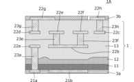
- FIG. 1 is a cross-sectional view showing the structure of each resin layer which is a part of the resin laminated substrate according to the first embodiment.
- FIG. 2 is a cross-sectional view of the resin laminate substrate 1 formed by hot pressing.
- FIG. 3 is a cross-sectional view of a resin laminated substrate 1A according to a first embodiment, which is different from the resin laminated substrate shown in FIG.
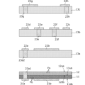
- FIG. 4 is a cross-sectional view showing the structure of each resin layer which is a part of the resin laminated substrate according to the second embodiment.
- FIG. 5 is a cross-sectional view showing the structure of each resin layer which is a part of the resin laminated substrate according to the third embodiment.
- FIG. 6 is a cross-sectional view of a resin laminated substrate 3 formed by hot pressing.
- FIG. 7 is a cross-sectional view showing the structure of each resin layer which is a part of the resin laminated substrate according to the fourth embodiment.
- FIG. 8 is a cross-sectional view of a resin laminated substrate 4 formed by laminating the resin layers shown in FIG. 7 and hot pressing them with a rigid member.
- FIG. 9 is a cross-sectional view of a resin laminated substrate 4A according to a fourth embodiment, which is different from the resin laminated substrate 4 shown in FIG.
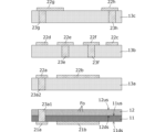
- FIG. 10 is a perspective view showing a structure of each resin layer which is a part of the resin laminated substrate according to the fifth embodiment.
- FIG. 11 is a cross-sectional view showing the structure of each resin layer which is a part of the resin laminated substrate according to the fifth embodiment.
- FIG. 12 is a cross-sectional view of a resin laminated substrate 5 formed by laminating the resin layers shown in FIG. 11 and hot pressing them with a rigid member.
- FIG. 13 is a cross-sectional view of a resin laminated substrate 5A according to a fifth embodiment, which is different from the resin laminated substrate shown in FIG.
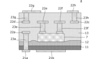
- First Embodiment Fig. 1 is a cross-sectional view showing the structure of each resin layer which is a part of the resin laminated substrate according to the first embodiment Fig. 2 is a cross-sectional view of the resin laminated substrate 1 formed by hot pressing.
- the resin laminated substrate 1 comprises a plurality of resin layers laminated on top of each other, and conductors disposed on the exterior and interior of the laminated resin layers.
- the first resin layer 11, the second resin layer 12, and the third resin layers 13a, 13b, and 13c are the above-mentioned "resin layers.”
- the first conductor layers 21a and 21b, the second conductor layers 22a to 22h, and the interlayer connecting conductors 23a1, 23a2, 23e, 23f, 23g, and 23h are the above-mentioned "conductors.”
- the first resin layer 11, the second resin layer 12, and the third resin layers 13a, 13b, and 13c are all made of LCP (liquid crystal polymer), PTFE (fluororesin), PI (polyimide), etc., but have different melting points.
- at least the second resin layer 12 is a thermoplastic resin.
- the first resin layer 11 has an upper main surface 11us and a lower main surface 11ds that face each other.
- the second resin layer 12 has an upper main surface 12us and a lower main surface 12ds that face each other.
- the upper principal surface 11us of the first resin layer 11 is in contact with the lower principal surface 12ds of the second resin layer 12.
- the first resin layer 11 and the second resin layer 12 are in direct contact with each other, and no conductor layer is disposed between the first resin layer 11 and the second resin layer 12.
- First conductor layers 21a and 21b are disposed on the lower main surface 11ds of the first resin layer 11.
- the third resin layer 13a is provided with an interlayer connection conductor 23a2 and a second conductor layer 22a that overlap the first conductor layer 21a when viewed in the thickness direction of the third resin layer 13a.
- the second conductor layer 22b is provided on the third resin layer 13a.
- Interlayer connection conductors 23e, 23f and second conductor layers 22e, 22f are arranged on the third resin layer 13b, overlapping the second conductor layer 22b when viewed in the thickness direction of the third resin layer 13b.
- second conductor layers 22c, 22d are arranged on the third resin layer 13b.
- An interlayer connection conductor 23g is arranged on the third resin layer 13c, overlapping the second conductor layer 22d when viewed in the thickness direction of the third resin layer 13c.
- An interlayer connection conductor 23h is also arranged on the third resin layer 13c.
- second conductor layers 22g and 22h are arranged on the third resin layer 13c, overlapping the interlayer connection conductors 23g and 23h.
- the second conductor layers 22b, 22e, 22f and the interlayer connection conductors 23e, 23f overlap the first conductor layer 21b when viewed in the thickness direction of the third resin layer.
- the second resin layer 12 is a thermoplastic resin, and the melting point of the second resin layer 12 is lower than the melting point of the first resin layer 11.
- the first resin layer 11 is a high-melting point resin
- the second resin layer 12 is a low-melting point resin.
- the melting point of the second resin layer 12 is lower than the heat press temperature, and the melting point of the first resin layer 11 is higher than the heat press temperature. Therefore, the second resin layer 12 becomes flexible earlier than the first resin layer 11 during heat press, and the air bubbles in the second resin layer 12 are filled with the second resin, effectively increasing the coplanarity of the outer surface of the first resin layer 11.
- the second resin layer 12 is a porous material having many air bubbles Fo. Therefore, when there is a partial pressure difference applied in the thickness direction of the second resin layer 12 during heat pressing, the amount of depression of the second resin layer 12 varies depending on the pressure. In other words, the more highly pressurized the second resin layer 12 is, the more it is depressed. Therefore, the second resin layer 12 can also be called a buffer layer (a layer with cushioning properties), a pressure relief layer, and an unevenness absorbing layer.
- the first resin layer 11 made of high melting point resin is pressurized during heat pressing while retaining high rigidity.
- the first resin layer 11, the second resin layer 12, and the third resin layers 13a, 13b, and 13c on which the conductor layers and interlayer connection conductors shown in FIG. 1 are formed are laminated and heat-pressed with a pressing member having a flat surface. That is, the pressing member presses and heats the first resin layer 11, the second resin layer 12, and the third resin layers 13a, 13b, and 13c of the laminate.
- FIG. 2 is a cross-sectional view of a resin laminate substrate 1 formed by stacking the resin layers shown in FIG. 1 and hot pressing them with a pressing member.
- the second resin layer 12, which is an inner layer, is a resin layer with a low melting point and is a resin layer of a thermoplastic porous material, rather than the first resin layer 11, which is the outermost layer.
- a resin laminate substrate 1 with high coplanarity on the side of the first resin layer, which is the outermost layer is obtained. Therefore, according to this embodiment, the coplanarity of the first conductor layer 21b formed on the outermost layer of the first resin layer 11 is improved.
- the third resin layers 13a, 13b, and 13c shown in FIG. 1 are integrated into the third resin layer 13.
- the second conductor layers 22g and 22h formed on the upper surface of the third resin layer 13c are embedded along the upper surface of the third resin layer 13.
- the upper surface of the resin laminate substrate 1 is flattened.
- the low-temperature resin absorbs the unevenness during heat pressing, making it possible to apply (equal) pressure to each interlayer connection conductor while maintaining the coplanarity of the surface layer. This reduces the unevenness of the stress applied to the conductor pattern in the outermost layer, improving the coplanarity of the conductor pattern in the outermost layer.
- the third resin layer made of a relatively high melting point resin maintains its rigidity during heat pressing, suppressing misalignment and sinking (buried amount) of the conductor pattern in the outermost layer, and improving the coplanarity of the conductor pattern in the outermost layer.
- the air in the bubbles of the first resin layer 11 easily flows into the bubbles of the second resin layer 12. This makes it easier for the second resin layer 12 to deform when pressurized, thereby maintaining the coplanarity of the outer surface of the first resin layer 11.
- the second resin layer 12 which is a low-melting point resin, is a thermoplastic resin, so it does not harden during heat pressing, the resin flows into the air bubbles with high efficiency, and the coplanarity of the outer surface of the first resin layer 11 is maintained.
- the resin flows into the air bubbles in the second resin layer to the extent that not all of the air bubbles are filled during heat pressing (air bubbles remain). Because the air bubble rate (the proportion of air bubbles in the resin, which can also be called the "air ratio") is high to that extent, the coplanarity of the conductor pattern on the outermost layer is improved in response to large differences in distribution density of the conductor layers.
- the air bubbles in the second resin layer 12 are crushed (resin is filled in the air bubbles) so that the air bubble content of the second resin layer 12 approaches the air bubble content of the first resin layer 11. This maintains high strength of the second resin layer and increases the rigidity of the entire resin laminate substrate.
- Examples of methods for forming a porous resin layer are as follows: (a) Compressed gas is mixed into heated resin to form bubbles. (b) A foaming agent is mixed into the resin, which is then heated to foam and form bubbles. (c) A solvent is mixed into the resin, which is then heated to vaporize the solvent, forming bubbles.
- FIG. 3 is a cross-sectional view of a resin laminated substrate 1A according to a first embodiment, which is different from the resin laminated substrate shown in FIG. 2.
- This resin laminated substrate 1A is constructed by forming a protective film 3a on the lower surface of the resin laminated substrate 1 shown in FIG. 2, and forming a protective film 3b on the upper surface of the resin laminated substrate 1.
- the configuration of the resin laminated substrate 1 in FIG. 3 is as shown in FIG. 2.
- the protective films 3a and 3b are provided, for example, by applying a solder resist. They can also be provided by attaching a coverlay layer such as PI (polyimide).
- conductor layer 22b is a signal conductor of the transmission line
- conductor layer 21b is an opposing ground conductor layer
- a microstrip line is formed by conductor layer 21b, conductor layer 22b, and parts of first resin layer 11, second resin layer 12, and third resin layer 13 between conductor layer 21b and conductor layer 22b.
- conductor layers 22e and 22f and interlayer connection conductors 23e and 23f function as signal lines for conductor layer 22b as a signal conductor.
- the coplanarity of the resin laminate substrate is improved, reducing the variation in the thickness of the resin layers above and below the transmission line portion, thereby suppressing the variation in the characteristic impedance of the transmission line.
- a resin laminate substrate having a transmission line is exemplified, but the present invention is not limited to this and can be applied to substrates having various conductor layers.
- a resin laminate substrate having an antenna function in which a radiating element is provided in the first resin layer 11 will be shown later.
- Second Embodiment In the second embodiment, a resin laminated substrate having a different configuration from that of the first resin layer 11 and the second resin layer 12 of the resin laminated substrate shown in the first embodiment will be illustrated.
- FIG. 4 is a cross-sectional view showing each resin layer structure which is a part of the resin laminate substrate according to the second embodiment.
- the second resin layer 12 is a porous material having many bubbles Fo, but in the second embodiment, the first resin layer 11 is also a porous material having many bubbles Fo.
- the second resin layer 12, which is a low-melting point resin has a higher bubble rate than the first resin layer 11, which is a relatively high-melting point resin. Therefore, when there is a partial pressure difference applied in the thickness direction of the first resin layer 11 and the second resin layer 12, the amount of depression of the first resin layer 11 and the second resin layer 12 differs depending on the pressure.
- both the first resin layer 11 and the second resin layer 12 can be called a buffer layer (a layer with cushioning properties), a pressure relaxation layer, and an unevenness absorption layer.
- the bubbles into which the resin flows during heat pressing are also arranged in the first resin layer 11, so that there are many escape routes for the molten resin. Therefore, by increasing the bubble ratio of the second resin layer 12, which is the low melting point resin side that is easily deformed, the bubbles are more likely to collapse. Also, as in the case of the first embodiment, the first resin layer 11 made of the high melting point resin is pressed while remaining highly rigid compared to the second resin layer during heat pressing. This is expected to improve the coplanarity of the outer surface of the first resin layer 11. Also, by making the bubble ratio of the second resin layer 12 relatively (relatively) high, the dielectric constant of this second resin layer 12 can be reduced. Therefore, the desired characteristic impedance can be obtained even if the line width is made thick. This also makes it possible to suppress the transmission loss in the signal transmission path.
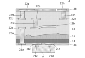
- FIG. 5 is a cross-sectional view showing the resin layer structure that is part of the resin laminate substrate according to the third embodiment.
- FIG. 6 is a cross-sectional view of the resin laminate substrate 3 formed by heat pressing.
- the resin laminated substrate 1 comprises a plurality of resin layers laminated on top of each other, and conductors disposed on the exterior and interior of the laminated resin layers.
- the first resin layer 11, the second resin layer 12, and the third resin layers 13a, 13b, and 13c are the above-mentioned "resin layers.”
- the first conductor layers 21a, 21c, and 21d, the second conductor layers 22a to 22h, and the interlayer connecting conductors 23a1, 23a2, 23e, 23g, and 23h are the above-mentioned "conductors.”
- the first resin layer 11 has an upper main surface 11us and a lower main surface 11ds that face each other.
- the second resin layer 12 has an upper main surface 12us and a lower main surface 12ds that face each other.
- the upper principal surface 11us of the first resin layer 11 is in contact with the lower principal surface 12ds of the second resin layer 12.
- First conductor layers 21a, 21c, and 21d are arranged on the lower main surface 11ds of the first resin layer 11.
- the third resin layer 13a is provided with an interlayer connection conductor 23a2 and a second conductor layer 22a that overlap the first conductor layer 21a when viewed in the thickness direction of the third resin layer 13a.
- the second conductor layer 22b is provided on the third resin layer 13a.
- An interlayer connection conductor 23e is arranged on the third resin layer 13b, overlapping with the second conductor layer 22b when viewed in the thickness direction of the third resin layer 13b. Also, a second conductor layer 22e is arranged on the third resin layer 13b, overlapping with the interlayer connection conductor 23e. Also, second conductor layers 22c and 22d are arranged on the third resin layer 13b.
- An interlayer connection conductor 23g is arranged on the third resin layer 13c, overlapping with the second conductor layer 22d when viewed in the thickness direction of the third resin layer 13c.
- An interlayer connection conductor 23h is also arranged on the third resin layer 13c.
- second conductor layers 22g and 22h are arranged on the third resin layer 13c, overlapping with the interlayer connection conductors 23g and 23h.
- the second resin layer 12 is a thermoplastic resin, and the melting point of the second resin layer 12 is lower than the melting point of the first resin layer 11.
- the first resin layer 11 is a high-melting point resin
- the second resin layer 12 is a low-melting point resin.
- the second resin layer 12 is a porous material that has many air bubbles Fo. Therefore, when there is a partial pressure difference applied in the thickness direction of the second resin layer 12 during heat pressing, the amount of depression varies depending on the pressure. In other words, the second resin layer 12 is more depressed in the areas that are subjected to higher pressure. Therefore, the second resin layer 12 can also be called a buffer layer (a layer with cushioning properties), a pressure relief layer, and an unevenness absorbing layer.
- the first resin layer 11 made of a high melting point resin is pressurized during heat pressing while retaining its high rigidity compared to the second resin layer.
- the first resin layer 11, the second resin layer 12, and the third resin layers 13a, 13b, and 13c, on which the conductor layers and interlayer connection conductors shown in FIG. 5 are formed, are laminated and heat-pressed with a rigid member having a flat surface.
- FIG. 6 is a cross-sectional view of a resin laminate substrate 3 formed by laminating the resin layers shown in FIG. 5 and hot pressing them with a rigid member to form a protective film 3a on the lower surface of the resin laminate substrate and a protective film 3b on the upper surface of the resin laminate substrate.
- the second resin layer 12, which is an inner layer, is a low-melting-point resin layer made of a thermoplastic porous material, rather than the first resin layer 11, which is the outermost layer.
- the conductor layer 22b deforms in response to the upward pressure from the conductor layers 21c and 21d, but a resin laminate substrate 3 is obtained in which the first resin layer 11 side, which is the outermost layer, and the first conductor layers 21c and 21d have high coplanarity.
- the terminals 71c, 71d of the electronic component 7 are mounted on the first conductor layers 21c, 21d by soldering or the like. Even when mounting electronic components on the outer surface of the resin laminate substrate 3 as in this embodiment, the high coplanarity of the first conductor layers 21c, 21d makes mounting the electronic component 7 easy and reliable.
- FIG. 7 is a cross-sectional view showing the resin layer structure that is part of the resin laminate substrate according to the fourth embodiment.
- FIG. 8 is a cross-sectional view of a resin laminate substrate 4 formed by stacking the resin layers shown in FIG. 7 and hot pressing them with a rigid member.
- the resin laminated substrate 4 comprises a plurality of resin layers laminated on top of each other, and conductors disposed on the exterior and interior of the laminated resin layers.
- the first resin layer 11, the second resin layer 12, and the third resin layers 13a, 13b, and 13c are the above-mentioned "resin layers.”
- the first conductor layers 21a and 21b, the second conductor layers 22a, 22c to 22h, and the interlayer connecting conductors 23a1, 23a2, 23e, 23f, 23g, and 23h are the above-mentioned "conductors.”
- First conductor layers 21a and 21b are disposed on the lower main surface of the first resin layer 11.
- the third resin layer 13a for inserting (embedding) the electronic components 7, and the electronic components 7 are inserted into the through holes.
- Terminals 71e, 71f of the electronic components 7 contact the interlayer connection conductors 23e, 23f.
- the first resin layer 11 has a first conductor layer 21b disposed in a position overlapping the electronic components 7 when viewed in the thickness direction of the first resin layer 11.
- the electronic components 7 are components such as ICs, chip capacitors, and chip inductors.
- the coplanarity of the first conductor layer 21b of the resin laminate substrate 4 can be maintained at a high level during heat pressing.
- the coplanarity of the outer surface of the resin laminate substrate deteriorates, but the presence of the second resin layer 12, which is a low-melting point resin layer, improves the coplanarity of the outer surface of the resin laminate substrate.
- FIG. 9 is a cross-sectional view of a resin laminated substrate 4A according to a fourth embodiment, which is different from the resin laminated substrate 4 shown in FIG. 8.
- This resin laminated substrate 4A is constructed by forming a protective film 3a on the lower surface of the resin laminated substrate 4 shown in FIG. 8, and forming a protective film 3b on the upper surface of the resin laminated substrate 4.
- the configuration of the resin laminated substrate 4 in FIG. 9 is as shown in FIG. 8.
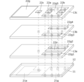
- FIG. 10 is a perspective view showing each resin layer structure that is a part of the resin laminated substrate according to the fifth embodiment.
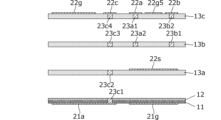
- FIG. 11 is a cross-sectional view showing each resin layer structure that is a part of the resin laminated substrate according to the fifth embodiment.
- FIG. 12 is a cross-sectional view of a resin laminated substrate 5 formed by stacking the resin layers shown in FIG. 11 and hot pressing them with a rigid member.
- the resin laminated substrate 1 comprises a plurality of resin layers laminated on top of each other, and conductors disposed on the exterior and interior of the laminated resin layers.
- the first resin layer 11, the second resin layer 12, and the third resin layers 13a, 13b, and 13c are the above-mentioned "resin layers.”
- the first conductor layers 21a and 21g, the second conductor layers 22g1, 22g2, 22g3, 22g4, 22g5, 22g, 22s, 22a, 22b, 22c, and 22s, and the interlayer connection conductors 23a1, 23a2, 23b1, 23b2, 23c1, 23c2, 23c3, and 23c4, etc. are the above-mentioned "conductors.”
- the second resin layer 12 is a thermoplastic resin, and the melting point of the second resin layer 12 is lower than the melting point of the first resin layer 11.
- the first resin layer 11 is a high-melting point resin
- the second resin layer 12 is a low-melting point resin.
- the second resin layer 12 is a porous material that has many air bubbles Fo. Therefore, when there is a partial pressure difference applied in the thickness direction of the second resin layer 12 during heat pressing, the amount of depression varies depending on that pressure.
- the first resin layer 11 made of a high melting point resin is pressurized during heat pressing while retaining its high rigidity compared to the second resin layer.
- the first conductor layer 21a is a radiating element, and the second conductor layer 22g is an opposing ground layer that faces the first conductor layer 21a.
- the first conductor layer 21a is electrically connected to the second conductor layer 22c via interlayer connection conductors 23c1, 23c2, 23c3, and 23c4.
- the first conductor layer 21a, the second conductor layers 22g and 22c, and the interlayer connection conductors 23c1, 23c2, 23c3, and 23c4 form a patch antenna.
- the second conductor layer 22s is a signal conductor, and the second conductor layers 22a and 22b are electrically connected to the second conductor layer 22s via the interlayer connection conductors 23a1, 23a2, 23b1, and 23b2.
- the second conductor layers 22s, 22a, and 22b and the interlayer connection conductors 23a1, 23a2, 23b1, and 23b2 form a microstrip line or a strip line.
- the second conductor layers 22g1, 22g2, 22g3, 22g4, and 22g5 and the interlayer connection conductors that connect them in the layer direction are at ground potential and act as shield electrodes that shield the microstrips.
- the dielectric constant of the first resin layer 11 with a high melting point, which is the outermost layer on which the conductor layer 21a, the radiating element, is formed, is higher than the dielectric constant of the second resin layer 12, which is an inner layer having holes. In this way, the high dielectric constant near the first conductor layer 21a, the radiating element, allows the antenna to be made smaller due to the wavelength compression effect.
- FIG. 13 is a cross-sectional view of a resin laminated substrate 5A according to a fifth embodiment, which is different from the resin laminated substrate shown in FIG. 12.
- This resin laminated substrate 5A is constructed by forming a protective film 3a on the lower surface of the resin laminated substrate 1 shown in FIG. 12, and forming a protective film 3b on the upper surface of the resin laminated substrate 1.
- the configuration of the resin laminated substrate 5 in FIG. 13 is as shown in FIG. 12.
- the variation in the distance between the first conductor layer 21a as the radiating element and the second conductor layer 22g as the opposing ground conductor layer is reduced, suppressing the variation in the resonant frequency of the antenna.
- the above effect can also be achieved by providing the second conductor layer as the radiating element on the second resin layer side and providing the first conductor layer as the opposing ground conductor layer on the first resin layer side.
- a conductor layer such as copper foil is provided on only one side of each resin layer prior to lamination by heat pressing.
- a conductor layer may be formed partially or entirely on both sides of a desired resin layer.
- a resin laminate substrate is exemplified in which the multiple resin layers include a first resin layer, a second resin layer, and a third resin layer that are laminated in order, and the first resin layer and the third resin layer are the outermost surfaces, but the first resin layer and the second resin layer may be provided on both sides of the resin laminate substrate.
- the resin laminate substrate may be constructed by laminating layers in the order of [first resin layer], [second resin layer], [third resin layer], [second resin layer], and [first resin layer], and then heat pressing.
- the resin laminate substrate and the method for producing the resin laminate substrate of the present invention may be provided in the following forms.
- the present invention includes a plurality of resin layers stacked on one another, and conductors disposed on the exterior and interior of the plurality of stacked resin layers,
- the plurality of resin layers include a first resin layer, a second resin layer, and a third resin layer which are laminated in order, the conductor includes a first conductor layer, a second conductor layer, and an interlayer connection conductor;
- the first resin layer has an upper main surface and a lower main surface opposed to each other,
- the second resin layer has an upper main surface and a lower main surface opposed to each other, the upper main surface of the first resin layer is in contact with the lower main surface of the second resin layer, the first conductor layer is disposed on the lower main surface of the first resin layer;
- the second conductor layer or the interlayer connection conductor is disposed in the third resin layer so as to overlap a portion of the first conductor layer when viewed in a thickness direction of the third resin layer;
- the second resin layer is a thermoplastic resin, and the melting point of the second resin
- the second resin layer has a higher void content than the first resin layer.
- the second conductor layer is disposed on the third resin layer, the second conductor layer overlapping at least a portion of the first conductor layer when viewed in the thickness direction of the third resin layer; At least a portion of the first conductor layer is a radiating element, and the second conductor layer overlapping at least a portion of the first conductor layer is a ground conductor. Alternatively, at least a part of the second conductor layer is a radiating element, and the first conductor layer overlapping at least a part of the second conductor layer is a ground conductor.
- the resin laminated substrate according to any one of ⁇ 1> to ⁇ 3>.
- the radiating element is disposed on the first resin layer, and the dielectric constant of the first resin layer is higher than the dielectric constant of the second resin layer; or the radiating element is disposed on the third resin layer, and the dielectric constant of the third resin layer is higher than the dielectric constant of the first resin layer.
- a protective film is formed on an outer surface of a laminate including the plurality of resin layers stacked on each other and the conductors disposed on the outside and inside of the plurality of stacked resin layers.
- an electronic component is disposed in the third resin layer at a position overlapping the first conductor layer;
- ⁇ 6> The resin laminated substrate according to any one of ⁇ 1> to ⁇ 6>.
- the lower main surface of the first resin layer is an outermost layer of a laminate including the plurality of resin layers stacked on each other and the conductors disposed on the outside and inside of the plurality of stacked resin layers, and a portion of the first conductor layer is disposed on the lower main surface of the first resin layer; ⁇ 8> The resin laminated substrate according to any one of ⁇ 1> to ⁇ 7>.
- the present invention includes a plurality of resin layers stacked on one another, and conductors disposed on the exterior and interior of the plurality of stacked resin layers,
- the plurality of resin layers include a first resin layer, a second resin layer, and a third resin layer which are laminated in order, the conductor includes a first conductor layer, a second conductor layer, and an interlayer connection conductor;
- the first resin layer has an upper main surface and a lower main surface opposed to each other,
- the second resin layer has an upper main surface and a lower main surface opposed to each other, the upper main surface of the first resin layer is in contact with the lower main surface of the second resin layer, the first conductor layer is disposed on the lower main surface of the first resin layer;
- the second conductor layer or the interlayer connection conductor is arranged in the third resin layer so as to overlap a part of the first conductor layer when viewed in a thickness direction of the third resin layer.
- a method for manufacturing a resin laminated substrate the second resin layer is a thermoplastic resin and has bubbles therein before the heat pressing;
- the melting point of the second resin layer is lower than the melting point of the first resin layer, a heat press performed on the first resin layer, the second resin layer, and the third resin layer in a laminated state at a temperature lower than a melting point of the first resin layer and higher than a melting point of the second resin layer;
- a method for manufacturing a resin laminated substrate is a thermoplastic resin and has bubbles therein before the heat pressing;
- the melting point of the second resin layer is lower than the melting point of the first resin layer, a heat press performed on the first resin layer, the second resin layer, and the third resin layer in a laminated state at a temperature lower than a melting point of the first resin layer and higher than a melting point of the second resin layer;
Landscapes
- Engineering & Computer Science (AREA)
- Microelectronics & Electronic Packaging (AREA)
- Manufacturing & Machinery (AREA)
- Production Of Multi-Layered Print Wiring Board (AREA)
Priority Applications (4)
| Application Number | Priority Date | Filing Date | Title |
|---|---|---|---|
| CN202480041790.XA CN121420631A (zh) | 2023-07-25 | 2024-06-03 | 树脂层叠基板以及树脂层叠基板的制造方法 |
| JP2025535605A JPWO2025022820A1 (https=) | 2023-07-25 | 2024-06-03 | |
| DE112024003086.6T DE112024003086T5 (de) | 2023-07-25 | 2024-06-03 | Harzlaminierplatte und verfahren zur herstellung einer harzlaminierplatte |
| US19/407,811 US20260089834A1 (en) | 2023-07-25 | 2025-12-03 | Resin laminated board and method for manufacturing resin laminated board |
Applications Claiming Priority (2)
| Application Number | Priority Date | Filing Date | Title |
|---|---|---|---|
| JP2023-120566 | 2023-07-25 | ||
| JP2023120566 | 2023-07-25 |
Related Child Applications (1)
| Application Number | Title | Priority Date | Filing Date |
|---|---|---|---|
| US19/407,811 Continuation US20260089834A1 (en) | 2023-07-25 | 2025-12-03 | Resin laminated board and method for manufacturing resin laminated board |
Publications (1)
| Publication Number | Publication Date |
|---|---|
| WO2025022820A1 true WO2025022820A1 (ja) | 2025-01-30 |
Family
ID=94374820
Family Applications (1)
| Application Number | Title | Priority Date | Filing Date |
|---|---|---|---|
| PCT/JP2024/020154 Pending WO2025022820A1 (ja) | 2023-07-25 | 2024-06-03 | 樹脂積層基板及び樹脂積層基板の製造方法 |
Country Status (5)
| Country | Link |
|---|---|
| US (1) | US20260089834A1 (https=) |
| JP (1) | JPWO2025022820A1 (https=) |
| CN (1) | CN121420631A (https=) |
| DE (1) | DE112024003086T5 (https=) |
| WO (1) | WO2025022820A1 (https=) |
Citations (3)
| Publication number | Priority date | Publication date | Assignee | Title |
|---|---|---|---|---|
| JPH07202439A (ja) * | 1993-12-27 | 1995-08-04 | Furukawa Electric Co Ltd:The | 高周波用多層回路基板 |
| WO2022260085A1 (ja) * | 2021-06-09 | 2022-12-15 | 株式会社村田製作所 | 多孔質樹脂シート、金属層付き多孔質樹脂シート、電子回路基板、多孔質樹脂シートの製造方法、金属層付き多孔質樹脂シートの製造方法、及び、電子回路基板の製造方法 |
| WO2022260094A1 (ja) * | 2021-06-09 | 2022-12-15 | 株式会社村田製作所 | 導体層付き樹脂フィルム、積層基板、及び、導体層付き樹脂フィルムの製造方法 |
Family Cites Families (2)
| Publication number | Priority date | Publication date | Assignee | Title |
|---|---|---|---|---|
| JP2005050860A (ja) * | 2003-07-29 | 2005-02-24 | Nitto Denko Corp | 多孔質配線板及びそれを用いた電子部品 |
| JP5927946B2 (ja) | 2011-02-14 | 2016-06-01 | 株式会社村田製作所 | 多層配線板の製造方法 |
-
2024
- 2024-06-03 WO PCT/JP2024/020154 patent/WO2025022820A1/ja active Pending
- 2024-06-03 JP JP2025535605A patent/JPWO2025022820A1/ja active Pending
- 2024-06-03 DE DE112024003086.6T patent/DE112024003086T5/de active Pending
- 2024-06-03 CN CN202480041790.XA patent/CN121420631A/zh active Pending
-
2025
- 2025-12-03 US US19/407,811 patent/US20260089834A1/en active Pending
Patent Citations (3)
| Publication number | Priority date | Publication date | Assignee | Title |
|---|---|---|---|---|
| JPH07202439A (ja) * | 1993-12-27 | 1995-08-04 | Furukawa Electric Co Ltd:The | 高周波用多層回路基板 |
| WO2022260085A1 (ja) * | 2021-06-09 | 2022-12-15 | 株式会社村田製作所 | 多孔質樹脂シート、金属層付き多孔質樹脂シート、電子回路基板、多孔質樹脂シートの製造方法、金属層付き多孔質樹脂シートの製造方法、及び、電子回路基板の製造方法 |
| WO2022260094A1 (ja) * | 2021-06-09 | 2022-12-15 | 株式会社村田製作所 | 導体層付き樹脂フィルム、積層基板、及び、導体層付き樹脂フィルムの製造方法 |
Also Published As
| Publication number | Publication date |
|---|---|
| DE112024003086T5 (de) | 2026-05-07 |
| US20260089834A1 (en) | 2026-03-26 |
| JPWO2025022820A1 (https=) | 2025-01-30 |
| CN121420631A (zh) | 2026-01-27 |
Similar Documents
| Publication | Publication Date | Title |
|---|---|---|
| JP3407737B2 (ja) | 多層基板の製造方法およびその製造方法によって形成される多層基板 | |
| US8178191B2 (en) | Multilayer wiring board and method of making the same | |
| JP4798237B2 (ja) | Ic搭載基板、及び多層プリント配線板 | |
| US10477704B2 (en) | Multilayer board and electronic device | |
| US8182729B2 (en) | Wiring board and method of making the same | |
| JP2026012559A (ja) | プリント配線板及びプリント配線板の製造方法 | |
| WO2025022820A1 (ja) | 樹脂積層基板及び樹脂積層基板の製造方法 | |
| JP6263167B2 (ja) | 多層基板および多層基板の製造方法 | |
| CN101322449A (zh) | 氟树脂层叠基板 | |
| JP3230727B2 (ja) | 多層プリント配線板及びその製造方法 | |
| JP6497486B2 (ja) | 多層基板およびその製造方法 | |
| JP2009206225A (ja) | 回路基板の製造方法 | |
| CN209676640U (zh) | 多层基板 | |
| JPH0359597B2 (https=) | ||
| JP4785473B2 (ja) | 多層プリント配線板、多層プリント配線板の製造方法、及び電子装置 | |
| JP2003168873A (ja) | 中空多層プリント配線基板 | |
| CN205491421U (zh) | 部件内置基板 | |
| CN221354668U (zh) | 多层基板 | |
| JPH10303553A (ja) | プリント配線板の製造方法 | |
| JP4803918B2 (ja) | 多層配線基板の製造方法 | |
| JP7234651B2 (ja) | 多層基板の製造方法 | |
| JP6750728B2 (ja) | 積層型電子部品および積層型電子部品モジュール | |
| JP2004221433A (ja) | 回路基板および多層配線回路基板の層間接続方法 | |
| JP2001085847A (ja) | 多層プリント配線基板製造方法及び多層プリント配線基板 | |
| JP4239423B2 (ja) | プリント基板の製造方法 |
Legal Events
| Date | Code | Title | Description |
|---|---|---|---|
| 121 | Ep: the epo has been informed by wipo that ep was designated in this application |
Ref document number: 24845202 Country of ref document: EP Kind code of ref document: A1 |
|
| ENP | Entry into the national phase |
Ref document number: 2025535605 Country of ref document: JP Kind code of ref document: A |
|
| WWE | Wipo information: entry into national phase |
Ref document number: 2025535605 Country of ref document: JP |
|
| WWE | Wipo information: entry into national phase |
Ref document number: 112024003086 Country of ref document: DE |