WO2025018006A1 - 積層セラミックコンデンサ - Google Patents
積層セラミックコンデンサ Download PDFInfo
- Publication number
- WO2025018006A1 WO2025018006A1 PCT/JP2024/017065 JP2024017065W WO2025018006A1 WO 2025018006 A1 WO2025018006 A1 WO 2025018006A1 JP 2024017065 W JP2024017065 W JP 2024017065W WO 2025018006 A1 WO2025018006 A1 WO 2025018006A1
- Authority
- WO
- WIPO (PCT)
- Prior art keywords
- length
- layer
- internal electrode
- inner layer
- width direction
- Prior art date
- Legal status (The legal status is an assumption and is not a legal conclusion. Google has not performed a legal analysis and makes no representation as to the accuracy of the status listed.)
- Pending
Links
Images


Classifications
-
- H—ELECTRICITY
- H01—ELECTRIC ELEMENTS
- H01G—CAPACITORS; CAPACITORS, RECTIFIERS, DETECTORS, SWITCHING DEVICES, LIGHT-SENSITIVE OR TEMPERATURE-SENSITIVE DEVICES OF THE ELECTROLYTIC TYPE
- H01G4/00—Fixed capacitors; Processes of their manufacture
- H01G4/30—Stacked capacitors
-
- H—ELECTRICITY
- H01—ELECTRIC ELEMENTS
- H01G—CAPACITORS; CAPACITORS, RECTIFIERS, DETECTORS, SWITCHING DEVICES, LIGHT-SENSITIVE OR TEMPERATURE-SENSITIVE DEVICES OF THE ELECTROLYTIC TYPE
- H01G4/00—Fixed capacitors; Processes of their manufacture
- H01G4/002—Details
- H01G4/005—Electrodes
- H01G4/012—Form of non-self-supporting electrodes
-
- H—ELECTRICITY
- H01—ELECTRIC ELEMENTS
- H01G—CAPACITORS; CAPACITORS, RECTIFIERS, DETECTORS, SWITCHING DEVICES, LIGHT-SENSITIVE OR TEMPERATURE-SENSITIVE DEVICES OF THE ELECTROLYTIC TYPE
- H01G4/00—Fixed capacitors; Processes of their manufacture
- H01G4/002—Details
- H01G4/018—Dielectrics
- H01G4/06—Solid dielectrics
- H01G4/08—Inorganic dielectrics
- H01G4/12—Ceramic dielectrics
-
- H—ELECTRICITY
- H01—ELECTRIC ELEMENTS
- H01G—CAPACITORS; CAPACITORS, RECTIFIERS, DETECTORS, SWITCHING DEVICES, LIGHT-SENSITIVE OR TEMPERATURE-SENSITIVE DEVICES OF THE ELECTROLYTIC TYPE
- H01G4/00—Fixed capacitors; Processes of their manufacture
- H01G4/002—Details
- H01G4/228—Terminals
- H01G4/232—Terminals electrically connecting two or more layers of a stacked or rolled capacitor
Definitions
- the present invention relates to a multilayer ceramic capacitor.
- Patent Document 1 discloses a technology in which a glass component is incorporated into the external electrodes.
- stacked dielectric sheets are pressed. This pressing can cause the dielectric layer to become thinner at the ends of the internal electrode layers.
- the edge effect causes the electric field strength to be greater than in other parts of the internal electrode layers. As a result, electric field concentration occurs at the ends of the internal electrode layers where the dielectric layer is thin, causing insulation breakdown.
- the objective of the present invention is to provide a multilayer ceramic capacitor that has high capacity while also being highly reliable.
- the multilayer ceramic capacitor of the present invention has a plurality of laminated dielectric layers, a plurality of first internal electrode layers and a plurality of second internal electrode layers laminated on the dielectric layers, and has a laminate having a first main surface and a second main surface facing each other in the lamination direction, a first end surface and a second end surface facing each other in a length direction perpendicular to the lamination direction, and a first side surface and a second side surface facing each other in a width direction perpendicular to the lamination direction and the length direction, a first external electrode disposed on the first end surface, and a second external electrode disposed on the second end surface,
- the device has an inner layer portion in which the plurality of first internal electrode layers and the plurality of second internal electrode layers face each other, and an outer layer portion made of a dielectric material, and when the length of the inner layer portion in a direction parallel to the stacking direction at the center position in the width direction is defined as a first length, and the length of the inner layer portion in
- the present invention provides a multilayer ceramic capacitor that is easy to improve in both capacity and reliability.
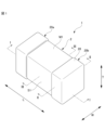
- FIG. 1 is a perspective view of a multilayer ceramic capacitor according to an embodiment of the present invention
- 2 is a cross-sectional view taken along line II in FIG. 1.
- 2 is a cross-sectional view taken along line II-II of FIG. 1.
- 3 is a cross-sectional view taken along line III-III in FIG. 1.
- 13 is a diagram showing a state in which a conductive paste and a step reducing paste are printed on a dielectric sheet.
- FIG. FIG. 2 is a diagram showing two dielectric sheets 40 to be laminated. This is a W-W' cross-sectional view of Figure 5A.
- Fig. 1 is a perspective view of a multilayer ceramic capacitor 1 according to an embodiment of the present invention.
- the laminate 2 includes a plurality of dielectric layers and a plurality of internal electrode layers that are stacked.
- the shape of the laminate 2 is approximately a rectangular parallelepiped.
- the direction in which the dielectric layers and the internal electrode layers are stacked is defined as the stacking direction T.
- the direction perpendicular to the stacking direction T is defined as the width direction W.
- the direction perpendicular to the stacking direction T and the width direction W is defined as the length direction L.
- one of the two surfaces facing each other in the stacking direction T is the first main surface M1.
- the remaining surface is the second main surface M2.
- one of the two surfaces facing each other in the width direction W is the first side surface S1.
- the remaining surface is the second side surface S2.
- one of the two surfaces facing each other in the length direction L is the first end surface E1.
- the remaining surface is the second end surface E2.
- the mounting surface of the multilayer ceramic capacitor 1 is the second main surface M2.
- the mounting surface refers to the surface that faces a wiring board when the multilayer ceramic capacitor 1 is mounted on a wiring board or the like.
- the cross section taken along line I-I in FIG. 1 is taken as the LT cross section.
- the cross section taken along line II-II in FIG. 1 is taken as the WT cross section.
- the cross section taken along line III-III in FIG. 1 is taken as the LW cross section.
- the corners and ridges of the laminate 2 are preferably rounded.
- the corners are the parts where three faces of the laminate 2 intersect.
- the ridges are the parts where two faces of the laminate 2 intersect.
- the main surface, side surfaces, and end surfaces may all or partly have irregularities.
- the total number of dielectric layers laminated in the laminate 2 is preferably 15 or more and 2000 or less.
- the main material of the dielectric layers is a ceramic material.
- the ceramic material include dielectric ceramics containing BaTiO 3 , CaTiO 3 , SrTiO 3 , CaZrO 3 or the like as main components.
- the ceramic material may be a dielectric ceramic containing these main components and additional components such as Mn compounds, Fe compounds, Cr compounds, Co compounds, Ni compounds or the like.
- each dielectric layer is preferably 0.5 ⁇ m or more and 10 ⁇ m or less.
- Fig. 2 is a cross-sectional view taken along line II in Fig. 1.
- the laminate 2 can be divided into a first main surface side outer layer portion OL1, an inner layer range IL, and a second main surface side outer layer portion OL2 in the stacking direction T.
- the first main surface side outer layer portion OL1, the inner layer range IL, and the second main surface side outer layer portion OL2 are arranged in this order from the first main surface M1 to the second main surface M2 in the stacking direction T.
- the first main surface side outer layer portion OL1 is the portion between the internal electrode layer closest to the first main surface M1 and the first main surface M1.
- the internal layer range IL is the range where the internal electrode layers face each other.
- the second main surface side outer layer portion OL2 is the portion between the internal electrode layer closest to the second main surface M2 and the second main surface M2.
- the first main surface side outer layer portion OL1 is located on the first main surface M1 side of the laminate 2.
- the first main surface side outer layer portion OL1 is formed by an assembly of multiple dielectric layers located between the first main surface M1 and the internal electrode layer closest to the first main surface M1.
- the first main surface side outer layer portion OL1 is formed by multiple dielectric layers located between the first main surface M1 and the outermost surface of the inner layer range IL on the first main surface M1 side and an extension of that outermost surface.
- the second main surface side outer layer portion OL2 is located on the second main surface M2 side of the laminate 2.
- the second main surface side outer layer portion OL2 is formed by an assembly of multiple dielectric layers located between the second main surface M2 and the internal electrode layer closest to the second main surface M2.
- the second main surface side outer layer portion OL2 is formed by multiple dielectric layers located between the second main surface M2 and the outermost surface of the inner layer range IL on the second main surface M2 side and an extension of that outermost surface.
- the inner layer range IL is the range sandwiched between the first main surface side outer layer portion OL1 and the second main surface side outer layer portion OL2.
- the dielectric layers disposed in the first main surface side outer layer portion OL1 and the second main surface side outer layer portion OL2 are referred to as outer dielectric layer 3.
- the dielectric layers disposed in the inner layer range IL are referred to as inner dielectric layer 4.
- the length in the length direction L is referred to as the length direction length.
- the length in the width direction W is referred to as the width direction length.
- the length in the stacking direction T is referred to as the stacking direction length.
- the position that is half the length direction length is referred to as the center position in the length direction L.
- the center position in the length direction L is referred to as the center position in the length direction.
- the position that is half the width direction length is referred to as the center position in the width direction W.
- the center position in the width direction W is referred to as the center position in the width direction.
- the position that is half the stacking length is referred to as the center position in the stacking direction T.
- the center position in the stacking direction T is referred to as the center position in the stacking direction.
- the end portions in the length direction L are referred to as the length direction end portions.
- the end portions in the width direction W are referred to as the width direction end portions.
- the end portions in the stacking direction T are referred to as the stacking direction end portions.
- the size of the laminate 2 is not particularly limited.
- the length of the laminate in the longitudinal direction is preferably 0.2 mm or more and 10 mm or less.
- the length of the laminate 2 in the width direction is preferably 0.1 mm or more and 5 mm or less.
- the length of the laminate 2 in the stacking direction is preferably 0.1 mm or more and 5 mm or less.
- the laminate 2 can be divided into a first end surface side outer layer portion LG1, a longitudinally facing portion LF, and a second end surface side outer layer portion LG2 in the longitudinal direction L.
- the first end surface side outer layer portion LG1, the longitudinally facing portion LF, and the second end surface side outer layer portion LG2 are arranged in this order in the longitudinal direction L from the first end surface E1 to the second end surface E2.
- the longitudinal opposing portion LF is the portion where the first internal electrode layer 6a and the second internal electrode layer 6b oppose each other in the stacking direction T.
- the first end face side outer layer portion LG1 is the portion between the longitudinal opposing portion LF and the first end face E1.
- the second end face side outer layer portion LG2 is the portion between the longitudinal opposing portion LF and the second end face E2.
- the longitudinal opposing portion LF is the portion corresponding to the opposing electrode portion of the internal electrode layer.
- the first end face side outer layer portion LG1 and the second end face side outer layer portion LG2 are the portions corresponding to the lead-out electrode portion of the internal electrode layer.
- the first end face side outer layer portion LG1 and the second end face side outer layer portion LG2 are also called L gaps.
- the first end face side outer layer portion LG1 is located on the first end face E1 side.
- the first end face side outer layer portion LG1 is located between the first end face E1 and the outermost surface of the end portion of the second internal electrode layer 6b on the first end face E1 side.
- the second end face side outer layer portion LG2 is located on the second end face E2 side.
- the second end face side outer layer portion LG2 is located between the second end face E2 and the outermost surface of the end portion of the first internal electrode layer 6a on the second end face E2 side.
- Fig. 3 is a cross-sectional view taken along line II-II in Fig. 1.
- the laminate 2 can be divided into a first side surface outer layer portion WG1, a widthwise opposing portion WF, and a second side surface outer layer portion WG2 in the width direction W.
- the first side surface outer layer portion WG1, the widthwise opposing portion WF, and the second side surface outer layer portion WG2 are arranged in this order in the width direction W from the first side surface S1 to the second side surface S2.
- the widthwise opposing portion WF is the portion where the internal electrode layers face each other in the stacking direction T.
- the first side surface side outer layer portion WG1 is the portion between the widthwise opposing portion WF and the first side surface S1.
- the second side surface side outer layer portion WG2 is the portion between the widthwise opposing portion WF and the second side surface S2.
- the first side surface side outer layer portion WG1 and the second side surface side outer layer portion WG2 are also called the W gap.
- the first side surface side outer layer portion WG1 and the second side surface side outer layer portion WG2 are portions where no internal electrode layer is present in the stacking direction T.
- the first side surface side outer layer portion WG1 is located on the first side surface S1 side.
- the first side surface side outer layer portion WG1 is formed by multiple dielectric layers located between the first side surface S1 and the outermost surface of the widthwise opposing portion WF on the first side surface S1 side.
- the second side surface outer layer portion WG2 is located on the second side surface S2 side.
- the second side surface outer layer portion WG2 is formed by multiple dielectric layers located between the second side surface S2 and the outermost surface of the widthwise opposing portion WF on the second side surface S2 side.
- the internal electrode layers include a plurality of first internal electrode layers 6a and a plurality of second internal electrode layers 6b.
- the first internal electrode layers 6a are internal electrode layers exposed at the first end face E1.
- the second internal electrode layers 6b are internal electrode layers exposed at the second end face E2.
- the first internal electrode layer 6a can be divided into a first opposing electrode portion 7a and a first extraction electrode portion 8a.
- the first opposing electrode portion 7a is a portion that faces the second internal electrode layer 6b.
- the first extraction electrode portion 8a is a portion that is extracted from the first opposing electrode portion 7a to the first end surface E1 of the laminate 2.
- the end of the first extraction electrode portion 8a on the first end face E1 side is extended to the surface of the first end face E1 of the laminate 2.
- the end of the first extraction electrode portion 8a extended to the first end face E1 forms an exposed portion at the first end face E1.
- the second internal electrode layer 6b can be divided into a second opposing electrode portion 7b and a second extraction electrode portion 8b.
- the second opposing electrode portion 7b is a portion that faces the first internal electrode layer 6a.
- the second extraction electrode portion 8b is a portion that is extracted from the second opposing electrode portion 7b to the second end face E2 of the laminate 2.
- the end of the second extraction electrode portion 8b on the second end face E2 side is extended to the surface of the second end face E2 of the laminate 2.
- the end of the second extraction electrode portion 8b extended to the second end face E2 forms an exposed portion at the second end face E2.
- the shapes of the first opposing electrode portion 7a and the second opposing electrode portion 7b are not particularly limited.
- the shapes of the first opposing electrode portion 7a and the second opposing electrode portion 7b are preferably rectangular.
- the corners of the first opposing electrode portion 7a and the corners of the second opposing electrode portion 7b may be rounded.
- the corners of the first opposing electrode portion 7a and the corners of the second opposing electrode portion 7b may be formed at an angle. Forming at an angle means forming them in a tapered shape.
- the shapes of the first and second extraction electrodes 8a and 8b are not particularly limited.
- the shapes of the first and second extraction electrodes 8a and 8b are preferably rectangular.
- the corners of the first and second extraction electrodes 8a and 8b may be rounded.
- the corners of the first and second extraction electrodes 8a and 8b may be formed at an angle. Forming at an angle means forming them in a tapered shape.
- the width of the first opposing electrode portion 7a and the width of the first extension electrode portion 8a may be the same. Either one of the width of the first opposing electrode portion 7a and the width of the first extension electrode portion 8a may be narrower than the remaining one.
- the width of the second opposing electrode portion 7b and the width of the second extension electrode portion 8b may be the same. Either one of the width of the second opposing electrode portion 7b and the width of the second extension electrode portion 8b may be narrower than the remaining one.
- the material of the first internal electrode layer 6a and the second internal electrode layer 6b can be an appropriate conductive material, such as a metal such as Ni, Cu, Ag, Pd, or Au, or an alloy containing at least one of these metals, such as an Ag-Pd alloy.
- the first opposing electrode portion 7a and the second opposing electrode portion 7b face each other via the inner dielectric layer 4, forming a capacitance. This allows the multilayer ceramic capacitor 1 to exhibit the characteristics of a capacitor.
- the thickness of the first internal electrode layer 6a and the second internal electrode layer 6b is preferably, for example, about 0.2 ⁇ m or more and 2.0 ⁇ m or less.
- the total number of the first internal electrode layers 6a and the second internal electrode layers 6b is preferably 15 or more and 2000 or less.
- a second dielectric layer 5b is disposed in the multilayer ceramic capacitor 1.
- the second dielectric layer 5b is a dielectric layer that is disposed in order to make the length of the laminate 2 in the lamination direction approximately uniform.
- the difference between the stacking direction length of the laminate 2 at the longitudinal opposing portion LF and the stacking direction length of the laminate 2 at the first end face side outer layer portion LG1 is small. It is preferable that the difference between the stacking direction length of the laminate 2 at the longitudinal opposing portion LF and the stacking direction length of the laminate 2 at the second end face side outer layer portion LG2 is small.
- the difference between the stacking direction length of the laminate 2 in the lengthwise opposing portion LF and the stacking direction length of the laminate 2 in the first end face side outer layer portion LG1 tends to be large.
- the difference between the stacking direction length of the laminate 2 in the lengthwise opposing portion LF and the stacking direction length of the laminate 2 in the second end face side outer layer portion LG2 tends not to be large.
- the inner layer dielectric layer 4 As well as the first internal electrode layer 6a and the second internal electrode layer 6b are laminated in the longitudinal opposing portion LF.
- the second internal electrode layer 6b is not laminated on the first end face side outer layer portion LG1.
- the layers stacked in the lengthwise opposing portion LF are different from those stacked in the first end face side outer layer portion LG1 and the second end face side outer layer portion LG2. Therefore, the stacking direction length is likely to differ between the lengthwise opposing portion LF and the first end face side outer layer portion LG1 and the second end face side outer layer portion LG2.
- an additional inner dielectric layer 4 is disposed on the first and second end face side outer layer portions LG1 and LG2.
- This additional inner dielectric layer 4 is referred to as the second dielectric layer 5b.
- the dielectric layer other than the second dielectric layer 5b included in the laminate 2 is referred to as the first dielectric layer 5a.
- the second dielectric layer 5b is disposed between the longitudinal end of the first internal electrode layer 6a and the second end face E2.
- the second dielectric layer 5b is disposed between the longitudinal end of the second internal electrode layer 6b and the first end face E1.
- the main component of the second dielectric layer 5b is preferably the same as the main component of the first dielectric layer 5a.
- the components of the second dielectric layer 5b are not limited to this.
- the second dielectric layer 5b is also disposed near the side surface.
- the lamination direction length of the laminate 2 is uniform not only in the length direction L but also in the width direction W.
- the lamination direction length tends to differ in the width direction W between the width direction opposing portion WF and the first side surface side outer layer portion WG1 and the second side surface side outer layer portion WG2, as in the length direction L.
- the inner layer dielectric layer 4 as well as the first internal electrode layer 6a and the second internal electrode layer 6b are laminated in the widthwise opposing portion WF.
- the first and second inner electrode layers 6a and 6b are not laminated on the first and second side outer layer portions WG1 and WG2. Only the inner dielectric layer 4 is laminated on the first and second side outer layer portions WG1 and WG2.
- the layers stacked in the widthwise opposing portion WF are different from those stacked in the first side outer layer portion WG1 and the second side outer layer portion WG2. Therefore, the stacking direction length is likely to differ between the widthwise opposing portion WF and the first side outer layer portion WG1 and the second side outer layer portion WG2.
- an additional inner dielectric layer 4 is disposed on the first and second side surface outer layer portions WG1 and WG2. This additional inner dielectric layer 4 is the second dielectric layer 5b.
- the second dielectric layer 5b is disposed between the ends of the first internal electrode layer 6a and the second internal electrode layer 6b on the side of the first side surface S1 in the width direction W and the first side surface S1.
- the second dielectric layer 5b is disposed between the ends of the first internal electrode layer 6a and the second internal electrode layer 6b on the side of the second side surface S2 in the width direction W and the second side surface S2.
- the portion where the first internal electrode layer 6a and the second internal electrode layer 6b face each other is defined as an inner layer portion 10.
- the inner layer portion 10 is a portion where the lengthwise facing portion LF shown in FIG. 2 and the widthwise facing portion WF shown in FIG. 3 intersect with the inner layer range IL.
- the shape of the inner layer portion 10 is approximately a rectangular parallelepiped.
- the portion where the lengthwise facing portion LF and the inner layer range IL intersect is shown as the inner layer portion 10.
- the portion where the widthwise facing portion WF and the inner layer range IL intersect is shown as the inner layer portion 10.
- the external electrodes include a first external electrode 20a and a second external electrode 20b.
- the first external electrode 20a is connected to the first internal electrode layer 6a.
- the first external electrode 20a is disposed from the first end face E1 to a part of the first main face M1 and a part of the second main face M2, as well as a part of the first side face S1 and a part of the second side face S2.
- the second external electrode 20b is connected to the second internal electrode layer 6b.
- the second external electrode 20b is also disposed on a portion of the first main surface M1 and a portion of the second main surface M2 from the second end face E2, as well as a portion of the first side surface S1 and a portion of the second side surface S2.
- the first external electrode 20a and the second external electrode 20b preferably have an underlying electrode layer and a plating layer.
- the underlying electrode layer may include at least one layer selected from a baked layer, a conductive resin layer, a thin film layer, etc.
- the conductive resin layer may be provided separately from the underlying electrode layer. An example will be described in which a baked layer is provided as the underlying electrode layer, and a conductive resin layer is provided separately from the underlying electrode layer.
- the first external electrode 20a includes a first base electrode layer 21a, a first conductive resin layer 22a, a first lower plating layer 23a, and a first upper plating layer 24a.
- the second external electrode 20b includes a second base electrode layer 21b, a second conductive resin layer 22b, a second lower plating layer 23b, and a second upper plating layer 24b.
- the first base electrode layer 21a and the second external electrode 20b are layers containing conductive metal and glass components.
- the first conductive resin layer 22a and the second conductive resin layer 22b do not contain metal components.
- the first conductive resin layer 22a and the second conductive resin layer 22b are formed of a thermosetting resin.
- the first lower plating layer 23a and the second lower plating layer 23b can be, for example, Ni plating layers.
- the first upper plating layer 24a and the second upper plating layer 24b can be, for example, Sn plating layers.
- the base electrode layer includes a first base electrode layer 21a and a second base electrode layer 21b.
- the first base electrode layer 21a is disposed from the first end face E1 to a part of the first main surface M1 and a part of the second main surface M2, as well as a part of the first side surface S1 and a part of the second side surface S2.
- the second base electrode layer 21b is disposed from the second end face E2 to a part of the first main surface M1 and a part of the second main surface M2, as well as a part of the first side surface S1 and a part of the second side surface S2.
- the first and second base electrode layers 21a and 21b contain a conductive metal and a glass component.
- the conductive metal is, for example, at least one of Cu, Ni, Ag, Pd, Ag-Pd alloy, Au, etc.
- the glass component is at least one of B, Si, Ba, Mg, Al, Li, etc.
- the first base electrode layer 21a and the second base electrode layer 21b may be formed in multiple layers.
- the first base electrode layer 21a and the second base electrode layer 21b may be formed by applying a conductive paste containing a glass component and a metal to the laminate and then baking it. This baking may be performed simultaneously with the baking of the internal electrode layer. This baking may be performed after the baking of the internal electrode layer.
- the first base electrode layer 21a and the second base electrode layer 21b are baked layers formed by baking.
- the thickness of the first base electrode layer 21a at the center position in the stacking direction of the first base electrode layer 21a located on the first end face E1 is preferably, for example, about 10 ⁇ m or more and 150 ⁇ m or less.
- the thickness of the second base electrode layer 21b at the center position in the stacking direction of the second base electrode layer 21b located on the second end face E2 is preferably, for example, about 10 ⁇ m or more and 150 ⁇ m or less.
- the thickness of the first and second underlying electrode layers 21a and 21b at the longitudinal center position of the first and second underlying electrode layers 21a and 21b located on the first and second main surfaces M1 and M2, and the first and second side surfaces S1 and S2 is, for example, about 5 ⁇ m or more and 50 ⁇ m or less.
- the thin film layer can be formed by a thin film formation method such as a sputtering method or a vapor deposition method.
- the formed thin film layer is a layer in which metal particles are deposited.
- the formed thin film layer has a thickness of 1 ⁇ m or less.
- a conductive resin layer is disposed on the base electrode layer.
- the conductive resin layer contains a resin component and a metal component.
- the conductive resin layer has a first conductive resin layer 22a and a second conductive resin layer 22b.
- the first conductive resin layer 22a and the second conductive resin layer 22b contain a thermosetting resin as a resin component.
- the base electrode layer does not contain a resin component.
- the base electrode layer contains a plating film, a metal component, a glass component, and the like.
- the base electrode layer is a fired product. For these reasons, the base electrode layer is not flexible.
- the conductive resin layer functions as a buffer layer. Therefore, when a bending stress is applied to the mounting board and this stress applies a physical impact to the multilayer ceramic capacitor 1, cracks are unlikely to occur in the multilayer ceramic capacitor 1. When a shock caused by a thermal cycle is applied to the multilayer ceramic capacitor 1, cracks are unlikely to occur in the multilayer ceramic capacitor 1.
- thermosetting resin contained in the conductive resin layer is, for example, various known thermosetting resins such as epoxy resin, phenolic resin, urethane resin, silicone resin, and polyimide resin.
- epoxy resin is one of the most suitable resins. This is because epoxy resin has excellent heat resistance, moisture resistance, and adhesion.
- the first conductive resin layer 22a is disposed on the first underlying electrode layer 21a.
- the first conductive resin layer 22a covers the first underlying electrode layer 21a. It is preferable that the end of the first conductive resin layer 22a is in contact with the laminate 2.
- the second conductive resin layer 22b is disposed on the second underlying electrode layer 21b.
- the second conductive resin layer 22b covers the second underlying electrode layer 21b. It is preferable that the end of the second conductive resin layer 22b is in contact with the laminate 2.
- the metal components contained in the first conductive resin layer 22a and the second conductive resin layer 22b can be Ag, Cu, Ni, Sn, Bi, or an alloy containing these.
- the shape of the metal components is preferably a filler shape.
- the metal components are metal powders, metal powders whose surfaces are coated with Sn, Ni, or Cu can be used.
- the metal powders are preferably powders of Ag, Cu, Ni, Sn, Bi, or alloys thereof.
- the metal components preferably contain Ag.
- Ag may be Ag alone.
- Ag may be an alloy containing Ag, or a metal powder whose surface is coated with Ag.
- Ag When using metal powder with an Ag coating on the surface, it is preferable to use powder of Cu, Ni, Sn, Bi or an alloy of these metals as the metal powder.
- Ag When Ag is used as the metal filler, there are the following advantages: Ag has the lowest resistivity of all metals. Ag can form electrodes with low electrical resistance. Ag is a precious metal. Ag is resistant to oxidation. Ag can increase the resistance of the conductive resin layer. Using Ag as the metal filler makes it possible to reduce the cost of the base metal while maintaining the properties of Ag.
- the shape of the metal filler contained in the first conductive resin layer 22a and the second conductive resin layer 22b is not particularly limited.
- the shape of the metal filler may be spherical or flat.
- the metal filler may be a mixture of spherical metal powder and flat metal powder.
- the average particle size of the metal filler contained in the first conductive resin layer 22a and the second conductive resin layer 22b is not particularly limited.
- the average particle size of the metal filler can be, for example, 0.3 ⁇ m or more and 10 ⁇ m or less.
- the average particle size of the metal filler contained in the conductive resin layer can be calculated using a laser diffraction particle size measurement method (based on IOS 13320). This method of calculating the average particle size can be applied regardless of the shape of the filler.
- the metal fillers contained in the first conductive resin layer 22a and the second conductive resin layer 22b allow the conductive resin layers to conduct electricity. Contact between the metal fillers forms a conductive path inside the conductive resin layers.
- the resins contained in the first conductive resin layer 22a and the second conductive resin layer 22b are various known thermosetting resins, such as epoxy resin, phenoxy resin, phenol resin, urethane resin, silicone resin, and polyimide resin.
- Epoxy resin has excellent heat resistance, moisture resistance, and adhesion. Epoxy resin is one of the most suitable resins.
- the first conductive resin layer 22a and the second conductive resin layer 22b preferably contain a curing agent in addition to the thermosetting resin.
- the curing agent can be any of various known compounds such as phenols, amines, acid anhydrides, imidazoles, active esters, and amide-imides.
- the amount of metal contained in the first conductive resin layer 22a is preferably 35 vmol% or more and 75 vmol% or less with respect to the total volume of the first conductive resin layer 22a.
- the amount of metal contained in the second conductive resin layer 22b is preferably 35 vmol% or more and 75 vmol% or less with respect to the total volume of the second conductive resin layer 22b.
- the amount of resin contained in the first conductive resin layer 22a is preferably 25 vmol% or more and 65 vmol% or less with respect to the total volume of the first conductive resin layer 22a.
- the amount of resin contained in the second conductive resin layer 22b is preferably 25 vmol% or more and 65 vmol% or less with respect to the total volume of the second conductive resin layer 22b.
- the thickness of the first conductive resin layer 22a or the second conductive resin layer 22b located on the first end face E1 or the second end face E2 at the center position in the stacking direction is preferably, for example, about 10 ⁇ m or more and 200 ⁇ m or less.
- the thickness of the conductive resin layer at the longitudinal center position of the first conductive resin layer 22a or the second conductive resin layer 22b located on the first main surface M1 and the second main surface M2, and the first side surface S1 and the second side surface S2 is preferably, for example, about 10 ⁇ m or more and 200 ⁇ m or less.
- the plating layer will be described.
- the plating layer includes a lower plating layer and an upper plating layer.
- the plating layer includes two layers.
- the plating layer may be a single layer or multiple layers.
- the lower-layer plating layer is disposed on the conductive resin layer.
- the lower-layer plating layer covers at least a portion of the conductive resin layer.
- the lower-layer plating layer includes a first lower-layer plating layer 23a and a second lower-layer plating layer 23b.
- the first lower-layer plating layer 23a is disposed on the first conductive resin layer 22a.
- the second lower-layer plating layer 23b is disposed on the second conductive resin layer 22b.
- the first underlayer plating layer 23a and the second underlayer plating layer 23b can be Ni plating layers. Using Ni plating layers for the underlayer plating layers prevents the underlayer electrode layer and the like from being eroded by solder when mounting the multilayer ceramic capacitor 1.
- the upper layer plating layer is disposed on the lower layer plating layer.
- the upper layer plating layer covers at least a portion of the lower layer plating layer.
- the upper layer plating layer includes a first upper layer plating layer 24a and a second upper layer plating layer 24b.
- the first upper layer plating layer 24a is disposed on the first lower layer plating layer 23a.
- the second upper layer plating layer 24b is disposed on the second lower layer plating layer 23b.
- the first upper plating layer 24a and the second upper plating layer 24b can be Sn plating layers.
- the solder wettability of the Sn plating layer is good. Therefore, using a Sn plating layer for the upper plating layer makes it easier to mount the multilayer ceramic capacitor 1 on a substrate, etc.
- the metals of the materials of the underlayer plating layer and the top plating layer are not particularly limited.
- the plating layers, including the underlayer plating layer and the top plating layer can be at least one of metals such as Cu, Ni, Ag, Pd, Au, and Sn, and alloys such as Ag-Pd alloys.
- each plating layer is preferably 2 ⁇ m or more and 15 ⁇ m or less.
- External electrodes can also be formed using only a plating layer. The following describes the case where only a plating layer is provided without providing a base electrode layer.
- the first external electrode 20a and the second external electrode 20b are formed directly on the surface of the laminate 2.
- the first external electrode 20a and the second external electrode 20b are plating layers.
- the multilayer ceramic capacitor 1 includes a plating layer electrically connected to the first internal electrode layer 6a or the second internal electrode layer 6b. Before forming the plating layer, a pretreatment can be performed. The pretreatment is, for example, disposing a catalyst on the surface of the laminate 2.
- the plating layer preferably includes a lower layer plating electrode and an upper layer plating electrode.
- the lower layer plating electrode is a plating electrode formed on the surface of the laminate 2.
- the upper layer plating electrode is a plating electrode formed on the surface of the lower layer plating electrode.
- the lower layer plating electrode and the upper layer plating electrode preferably include at least one metal selected from, for example, Cu, Ni, Sn, Pb, Au, Ag, Pd, Bi, and Zn, or an alloy containing the metal.
- the lower layer plated electrode is preferably formed using Ni. Ni has good solder barrier performance.
- the upper layer plated electrode is preferably formed using Sn or Au. Sn and Au have good solder wettability.
- the lower layer plating electrode is formed using Cu.
- Cu has good bonding with Ni.
- the upper layer plating electrode can be formed as necessary.
- the first external electrode 20a and the second external electrode 20b may be formed only by the lower layer plating electrode.
- the outermost layer of the plating layer may be an upper layer plating electrode. Another plating electrode may be formed on the surface of the upper layer plating electrode.
- the preferred thickness of each plating layer is 1 ⁇ m or more and 15 ⁇ m or less. It is preferred that the plating layer does not contain glass.
- the preferred metal ratio per unit volume of the plating layer is 99 volume % or more.
- the size of the multilayer ceramic capacitor 1 is not particularly limited.
- the preferred length in the longitudinal direction of the multilayer ceramic capacitor 1 including the laminate 2 and the external electrodes is 0.2 mm or more and 10 mm or less.
- the preferred length in the lamination direction of the multilayer ceramic capacitor 1 including the laminate 2 and the external electrodes is 0.1 mm or more and 5 mm or less.
- the preferred length in the width direction of the multilayer ceramic capacitor 1 including the laminate 2 and the external electrodes is 0.1 mm or more and 10 mm or less.
- the conductive paste for the dielectric sheet and the internal electrode layer contains a binder and a solvent.
- the binder and the solvent may be a known organic binder and an organic solvent, etc.
- a conductive paste for the internal electrode layer is printed in a predetermined pattern on the dielectric sheet.
- the internal electrode layer pattern is formed by printing the conductive paste.
- the printing can be performed by, for example, screen printing or gravure printing.
- a predetermined number of dielectric sheets for the outer layer are stacked. No internal electrode layer pattern is printed on the dielectric sheets for the outer layer. Dielectric sheets with internal electrode layer patterns printed on them are stacked in order on top of the stacked dielectric sheets. Furthermore, a predetermined number of dielectric sheets for the outer layer are stacked on top of them. A laminated sheet is produced by stacking these layers.
- the second dielectric layer 5b will now be described.
- the second dielectric layer 5b is arranged to reduce the step in the laminate 2.
- the dielectric paste that becomes the second dielectric layer 5b is called step reduction paste.
- the step-reducing paste is applied to the area surrounding the internal electrode layer pattern on the dielectric sheet on which the internal electrode layer pattern is printed.
- the step-reducing paste is applied to the area where the internal electrode layer pattern is not formed. This is because the step-reducing paste is a paste used to eliminate the step between the internal electrode layer pattern and its surrounding area.
- the step-reducing paste can be applied so as to overlap the end of the internal electrode layer pattern.
- the overlap width can be, for example, about 50 ⁇ m.
- the step-reducing paste can be applied so as to form a gap between the internal electrode layer pattern and the step-reducing paste.
- the gap width can be, for example, 50 ⁇ m.
- the step-reducing paste may be the same as the ceramic paste used when producing the dielectric sheet.
- the step-reducing paste may be different from the ceramic paste used when producing the dielectric sheet.
- the laminated sheets are pressed in the stacking direction to produce a laminated block.
- the pressing method can be isostatic pressing.
- the laminated block is cut to a predetermined size. This cutting process cuts out laminated chips. When cutting, the corners and edges of the laminated chips may be rounded. Barrel polishing may be used to round them.
- the laminated chip is fired. This firing produces a laminate.
- the preferred firing temperature is 900°C or higher and 1200°C or lower. The firing temperature can be changed depending on the materials of the dielectric and internal electrode layers.
- the laminate is provided with external electrodes.
- a conductive paste that will become the base electrodes is applied to both end surfaces of the laminate.
- the conductive paste contains a glass component and a metal.
- the application method can be, for example, a dipping method.
- a baking process is performed.
- a base electrode layer is formed by this baking process.
- the preferred temperature for the baking process is 700° C. or higher and 900° C. or lower.
- the base electrode layer is a baked layer.
- the conductive resin layer is formed on the base electrode layer.
- a conductive resin paste is prepared.
- the conductive resin paste contains a resin component and a metal component.
- the conductive resin paste is applied onto the base electrode layer.
- the application method can be a dipping method.
- a heat treatment is performed.
- the temperature of the heat treatment is 200°C or higher and 550°C or lower.
- the resin is thermally cured by this heat treatment.
- the conductive electrode layer is formed by this thermal curing.
- the atmosphere during the heat treatment is preferably a nitrogen gas atmosphere.
- the preferred oxygen concentration is 100 ppm or lower. This oxygen concentration makes it difficult for the resin to scatter. This oxygen concentration makes it difficult for various metal components to oxidize.
- Ni plating layer is formed on the surface of the conductive resin layer.
- This Ni plating layer becomes the first underlayer plating layer and the second underlayer plating layer.
- the method for forming the Ni plating layer can be an electrolytic plating method.
- a preferred plating method is barrel plating.
- a Sn plating layer is formed on the Ni plating layer.
- a first Sn plating layer is formed on the first Ni plating layer.
- a second Sn plating layer is formed on the second Ni plating layer.
- Reference numeral 101 in Fig. 4 is a cross-sectional view taken along line III-III in Fig. 1.
- Reference numeral 101 in Fig. 4 is a WT cross-sectional view of the laminate 2 at the center position in the longitudinal direction of the laminate 2.
- the lamination direction length of the inner layer section 10 will be described.
- the width direction length of the inner layer section 10 is indicated by length D7.
- the width direction end of the inner layer section 10 is indicated by line W3.
- Half the length of length D7 is length D8.
- a position that is a length D8 away from the width direction end W3 in the direction of the other width direction end in the width direction W of the inner layer section 10 is indicated by line W1.
- the position of line W1 is the center position in the width direction.
- the length equivalent to 0.3% to 8.0% of length D7 is defined as length D9.
- a position where the length from an end of the width direction W of the inner layer portion 10 in a direction parallel to another end of the width direction W of the inner layer portion 10 is 0.3% to 8.0% of the length in the width direction W of the inner layer portion 10 is included in the range of length D9.
- a position that is a length D9 away from the width direction end W3 in the direction of the other width direction end in the width direction W of the inner layer portion 10 is indicated by line W2.
- the position of line W2 is defined as end vicinity position W2 in the width direction W of the inner layer portion 10. End vicinity position W2 in the width direction W is defined as width direction end vicinity position W2.
- the length in the stacking direction of the inner layer section 10 at the widthwise center position W1 is defined as the first length D1.
- the length in the stacking direction of the inner layer section 10 at the widthwise end position W2 is defined as the second length D2.
- the length in the stacking direction of the inner layer section 10 at the widthwise end position W3 is defined as the third length D3.
- the second length D2 is longer than the first length D1.
- the stacking direction length of the inner layer section 10 is longer at the widthwise end vicinity position W2 than at the widthwise central position W1.
- the second length D2 is 102.6% or less of the first length D1. Or, the second length D2 is longer than the first length D1, and the difference between the second length D2 and the first length D1 is 30 ⁇ m or less.
- the third length D3 is shorter than the first length D1.
- the stacking direction length of the inner layer section 10 is shorter at the widthwise end portion W3 than at the widthwise central position W1.
- the stacking direction length of the inner layer 10 is: widthwise end vicinity position W2 > widthwise central position W1 > widthwise end position W3.
- the width direction length of the inner layer portion 10 will be explained. It is indicated by the stacking direction length D10 of the inner layer portion 10. The stacking direction end of the inner layer portion 10 is indicated by line T6. Half the length of length D10 is length D11. Line T4 indicates a position that is a length D11 away from stacking direction end T6 in the direction of the other stacking direction end of the inner layer portion 10 in the stacking direction T. The position of line T4 is the center position in the stacking direction.
- length D12 The length equivalent to 10% to 40% of length D10 is defined as length D12.
- a position that is a length D12 away from stacking direction end T6 in the direction of another stacking direction end of the inner layer portion 10 in the stacking direction T is indicated by line T5.
- the position of line T5 is defined as position T5 near the stacking direction end of the inner layer portion 10.
- the widthwise length of the inner layer 10 at the central position T4 in the stacking direction is defined as a fourth length D4.
- the widthwise length of the inner layer 10 at the position T5 near the end of the stacking direction is defined as a fifth length D5.
- the widthwise length of the inner layer 10 at the end T6 in the stacking direction is defined as a sixth length D6.
- the fifth length D5 is shorter than the fourth length D4.
- the width direction length of the inner layer portion 10 is shorter at the position T5 near the end in the stacking direction than at the center position T4 in the length direction.
- the fifth length D5 is 97.5% or more and less than 100% of the fourth length D4. Or, the fifth length D5 is longer than the fourth length D4, and the difference between the fifth length D5 and the fourth length D4 is 30 ⁇ m or less.
- the sixth length D6 is shorter than the fifth length D5.
- the width direction length of the inner layer portion 10 is shorter at the end T6 in the stacking direction than at the position T5 near the end in the stacking direction.
- the width direction length of the inner layer 10 is the stacking direction central position T4 > stacking direction end vicinity position T5 > stacking direction end T6.
- FIG. 4 is a diagram showing an enlarged view of a part of the inner layer portion 10.
- the first inner electrode layer 6a and the second inner electrode layer 6b are raised in the direction of the first inner electrode layer M1 from the second inner electrode layer M2 in the stacking direction T.
- a portion of the inner electrode layer located closer to the first inner electrode layer M1 at the width direction end vicinity position W2 than the position on the first inner electrode layer M1 side in the stacking direction T at the width direction center position W1 is defined as a raised portion 30.
- the raised portion 30 is formed by the inner electrode layer overlapping the second dielectric layer 5b. Due to the presence of the raised portion 30, the stacking direction length at the width direction end vicinity position W2 of the inner layer portion 10 is longer than the stacking direction length at the width direction center position W1.
- the stacking direction length of each layer will be described based on 102 in Fig. 4.
- the stacking direction length of each layer indicates the thickness of each layer.
- the stacking direction length of the dielectric layers will be described.
- the stacking direction length of the first dielectric layer 5a at the widthwise center position W1 is length D21.
- the stacking direction length of the second dielectric layer 5b at the widthwise end vicinity position W2 is length D22.
- the stacking direction length of the second dielectric layer 5b at the widthwise end W3 is length D23.
- the length of the dielectric layer in the stacking direction is longer at position W2 near the widthwise end than at position W11 in the widthwise center.
- Length D22 is longer than length D21.
- the length of the dielectric layer in the stacking direction is longer at the widthwise end W3 than at the position W2 near the widthwise end.
- Length D23 is longer than length D22.
- the stacking direction length of the internal electrode layer will be described.
- the internal electrode layer will be described using the first internal electrode layer 6a as an example.
- the contents described using the first internal electrode layer 6a as an example are similar to those for the second internal electrode layer 6b.
- the stacking direction length at the widthwise center position W1 of the first internal electrode layer 6a is length D24.
- the stacking direction length at the widthwise end vicinity position W2 of the first internal electrode layer 6a is length D25.
- the stacking direction length at the widthwise end W3 of the first internal electrode layer 6a is length D26.
- the length in the stacking direction of the first internal electrode layer 6a is shorter at the position W2 near the widthwise end than at the center position W1 in the widthwise direction.
- Length D25 is shorter than length D24.
- the lamination direction length of the first internal electrode layer 6a is shorter at the widthwise end W3 than at the position W2 near the widthwise end.
- Length D26 is shorter than length D25.
- One dielectric layer and one internal electrode layer in contact with this dielectric layer are combined to form one element.
- the sum of the stacking direction length of the dielectric layers included in one element and the stacking direction length of the internal electrode layers included in one element is the stacking direction length of the element.
- the stacking direction length of the element at the widthwise center position W1 is the sum of lengths D21 and D24.
- the stacking direction length of the element at the widthwise end vicinity position W2 is the sum of lengths D22 and D25.
- the stacking direction length of the element at the widthwise end W3 is the sum of lengths D23 and D26.
- the increase in length D22 of the dielectric layer from length D21 is greater than the decrease in length D25 of the internal electrode layer from length D24. Therefore, the stacking direction length of the element is longer at the widthwise end vicinity position W2 than at the widthwise center position W1. As a result, the stacking direction length of the inner layer portion 10 is longer at the widthwise end vicinity position W2 than at the widthwise center position W1.
- the increase in length D23 of the dielectric layer from length D21 is smaller than the decrease in length D26 of the internal electrode layer from length D24. Therefore, the stacking direction length of the element is shorter at the width direction end W3 than at the width direction center position W1. As a result, the stacking direction length of the inner layer portion 10 is shorter at the width direction end W3 than at the width direction center position W1.
- the second length D2 is longer than the first length D1, so that the capacitance of the multilayer ceramic capacitor 1 can be increased.
- the lamination direction length of the internal electrode layer included therein at the width direction end vicinity position W2 can be lengthened.
- the capacitance increases.
- the lamination direction length of the internal electrode layer does not suddenly decrease in two stages from the width direction center position W1 to the width direction end position W3 from the width direction center position W1 to the width direction end position W3.
- the lamination direction length of the internal electrode layer becomes a length D25 longer than the length D26 at the width direction end position W3 at the width direction end vicinity position W2 between the width direction center position W1 and the width direction end position W3. This is because the existence of the protuberance 30 increases the lamination direction length of the internal electrode layer at the width direction end vicinity position W2.
- the length of the internal electrode layer in the stacking direction is longer at position W2 near the widthwise end than at widthwise end W3. This allows the inner layer 10 to generate a larger capacitance.
- the laminate sheet may be pressed in the stacking direction T. This pressing may cause the stacking direction length of the inner layer portion 10 to be shorter at the widthwise end W3 than at the widthwise center position W1. If the stacking direction length of the inner layer portion 10 at the widthwise end W3 becomes shorter, the reliability of the multilayer ceramic capacitor 1 may decrease. In order to prevent the stacking direction length of the inner layer portion 10 at the widthwise end W3 from becoming shorter, the stacking direction length of the inner layer portion 10 at the widthwise center position W1 may be increased. In order to increase the stacking direction length of the inner layer portion 10 at the widthwise center position W1, for example, it is possible to increase the stacking direction length of the dielectric layer. Increasing the stacking direction length of the dielectric layer is a factor that reduces the electrostatic capacitance of the multilayer ceramic capacitor 1.
- the multilayer ceramic capacitor 1 at the position W2 near the widthwise end, a portion is formed where the lamination direction length of the inner layer portion 10 is longer than at the widthwise end W3. This makes it possible to suppress a decrease in the length of the inner layer portion 10 at the widthwise end W3. This means that there is no need to increase the lamination direction length of the inner layer portion 10 at the widthwise center position W1. This means that there is no need to increase the lamination direction length of the dielectric layer. This makes it possible to increase the capacitance of the multilayer ceramic capacitor 1.
- the second length D2 is longer than the first length D1, thereby improving the electrical strength of the multilayer ceramic capacitor 1.
- the multilayer ceramic capacitor 1 may be exposed to a strong electric field, particularly at the ends. When the multilayer ceramic capacitor 1 is exposed to a strong electric field, dielectric breakdown may occur in the multilayer ceramic capacitor 1.
- the lamination direction length of the dielectric layer is longer at a widthwise end vicinity position W2 than at a widthwise central position W1. Furthermore, at a widthwise end position W3, the lamination direction length of the dielectric layer is longer than at a widthwise end vicinity position W2.
- the multilayer ceramic capacitor 1 disclosed herein has increased strength against electric fields, especially at the ends.
- FIG. 5A is a diagram showing the state in which conductive paste 42 for internal electrode layers and step reduction paste 44 are printed on a dielectric sheet.
- Figure 5A is a top view of a surface parallel to the length direction L and width direction W.
- Figure 5B is a diagram showing two dielectric sheets 40 to be laminated.
- Figure 6 is a W-W' cross-sectional view of Figure 5A.
- a conductive paste 42 for the internal electrode layer is printed in a predetermined pattern on the dielectric sheet.
- the dielectric sheet is not shown in FIG. 5A.
- the dielectric sheet 40 is shown in FIG. 5B and FIG. 6.
- recessed portions 50 are provided at both widthwise ends near the center position in the length direction.
- the recessed portions 50 refer to portions where a part of the outline of the internal electrode layer pattern is cut out.
- the structure of the internal electrode layer pattern provided with the recessed portions 50 is also called a racket structure. Note that the internal electrode layer pattern is not limited to this racket structure. Also, the internal electrode layer pattern may be a pattern in which the recessed portions 50 are not provided.
- a step-reducing paste 44 is arranged around the pattern of the conductive paste 42 for the internal electrode layers.
- the step-reducing paste 44 is printed on the dielectric sheet 40 before the conductive paste 42 for the internal electrode layers is printed on the dielectric sheet 40.
- the conductive paste 42 for the internal electrode layers is printed so that a portion of it overlaps the step reduction paste 44.
- An explanation will be given based on FIG. 6.
- the width direction length of the portion where the conductive paste 42 for the internal electrode layers overlaps the conductive paste 44 is indicated by length D31.
- Length D31 is called the overlap length.
- the length of overlap length D31 can be determined appropriately.
- the length of overlap length D31 can be set to, for example, 50 ⁇ m.
- the configuration shown in FIG. 6 in which the conductive paste 42 overlaps the step-reducing paste 44 means that the conductive paste 42 is formed after the step-reducing paste 44 is formed. If the conductive paste 42 is formed after the step-reducing paste 44 is formed, the positions of the ends of the internal electrode layers in the length direction L in the subsequent laminate 2 tend to be aligned. This is because the step-reducing paste 44 acts as a dam for the conductive paste 42 when the conductive paste 42 is formed.
- the order of forming the step-reducing paste 44 and the conductive paste 42 may be such that the conductive paste 42 is formed first, followed by the step-reducing paste 44. Even with this order of formation, it is possible to obtain a multilayer ceramic capacitor 1 having the preferred first length D1 and second length D2.
- the portion where the conductive paste 42 for the internal electrode layer overlaps the step reduction paste 44 is called the overlapping portion 46.
- This overlapping portion 46 becomes the raised portion 30 in the inner layer portion 10, shown as 102 in FIG. 4.
- Length D32 in FIG. 6 indicates the printing thickness of the step-reducing paste 44.
- Length D33 in FIG. 6 indicates the printing thickness of the conductive paste 42 for the internal electrode layer.
- Lengths D32 and D33 can be set appropriately.
- the ratio of length D32 to length D33, i.e., D32/D33, can be set to, for example, 0.5.
- the length in the width direction W of the inner layer 10 can be manufactured so that D6 ⁇ D5 ⁇ D4 by stacking the inner layer 10 loosely without any countermeasures against unevenness, and then using a rubber press to locally push the outer layer into the gap.
- FIG. 5B With reference to FIG. 5B, the lamination of the dielectric sheets 40 on which the conductive paste 42 for the internal electrode layers is printed will be described.
- two dielectric sheets 40 are shown to explain the lamination method.
- a predetermined number of dielectric sheets 40 are laminated in sequence using the lamination method shown in FIG. 5B.
- the dielectric sheets 40 are stacked with every other sheet shifted in the length direction L.
- the two dielectric sheets 40 stacked consecutively are the first dielectric sheet 40A and the second dielectric sheet 40B.
- the second dielectric sheet 40B is stacked on the first dielectric sheet 40A in a state where it is shifted in the length direction L by approximately half the length of the dielectric sheet 40 in the length direction L with respect to the first dielectric sheet 40A.
- the laminate in which a predetermined number of dielectric sheets 40 are stacked, is cut at predetermined locations.
- the cutting positions are indicated by lines L1 and L2. After cutting, the cut pieces are fired to obtain the laminate 2.
- the conductive paste 42 for the internal electrode layer printed on the first dielectric sheet 40A becomes the first internal electrode layer 6a.
- the conductive paste 42 for the internal electrode layer printed on the second dielectric sheet 40B becomes the second internal electrode layer 6b.
- the starting points where the length in the width direction W becomes shorter are the first recess end 51 and the second recess end 52.
- the first recess end 51 and the second recess end 52 are located opposite each other in the width direction W.
- the line connecting the first recess end 51 and the second recess end 52 is indicated by line L3.
- the ends in the length direction L are the first square end 53 and the second square end 54.
- the first square end 53 and the second square end 54 are located opposite each other in the width direction W.
- the line connecting the first square end 53 and the second square end 54 is indicated by line L4.
- the first dielectric sheet 40A and the second dielectric sheet 40B are laminated so that the lines L3 and L4 do not overlap.
- the direction in which the line L3 is shifted from the line L4 is the direction in which the line L3 does not overlap the conductive paste 42 for the internal electrode layer printed on the dielectric sheet 40 to be laminated.
- the line L3 is shifted in the direction in which the line L3 on the first dielectric sheet 40A does not overlap the conductive paste 42 for the internal electrode layer printed on the second dielectric sheet 40B.
- the length by which the lines L3 and L4 are shifted is shown as length D50.
- the dielectric sheets 40 are laminated so that the lines L3 and L4 do not overlap. Therefore, in the laminate 2 after firing, the internal electrode layers are as follows. Below, the internal electrode layers will be described with reference to FIG. 5B, assuming that the conductive paste 42 for the internal electrode layers shown in FIG. 5B becomes the internal electrode layers by firing. In FIG. 5B, the reference numerals for the internal electrode layers are in parentheses.
- the first extraction electrode portion 8a of the first end face side outer layer portion LG1 has a portion whose length in the width direction W is the same as that of the first opposing electrode portion 7a of the longitudinal opposing portion LF.
- the portion indicated by length D50 is the portion where the length in the width direction W of the first extraction electrode portion 8a is the same as the length in the width direction W of the first opposing electrode portion 7a.
- the length in the width direction W of the first opposing electrode portion 7a of the longitudinal opposing portion LF is indicated by length D51.
- the length in the width direction W of the first lead electrode portion 8a of the first end face side outer layer portion LG1 is indicated by length D52 within the range indicated by D50.
- the length in the width direction W of the first lead electrode portion 8a of the first end face side outer layer portion LG1 on line L1 is indicated by D53.
- Line L1 is a line corresponding to the end face of the laminate 2.
- D52 is equal to D51.
- D53 is shorter than D51 and D52. This is because a recess 50 is formed.
- the length of each portion of the multilayer ceramic capacitor 1, the laminate 2, the inner layer portion 10, etc. can be measured with a micrometer or an optical microscope.
- the multilayer ceramic capacitor 1 is polished to a desired position, such as the center position in the longitudinal direction. Then, the cross section exposed by polishing can be observed with an optical microscope or the like to measure the length.
- the step reducing paste 44 may be printed on the dielectric sheet 40 after the conductive paste 42 for the internal electrode layers is printed on the dielectric sheet 40 .
- the overlap between the conductive paste 42 for the internal electrode layers and the step reducing paste 44 may be provided on the sides along the width direction W in addition to the sides along the length direction L in the outline of the internal electrode layer pattern.
- a laminate having a plurality of laminated dielectric layers, a plurality of first internal electrode layers and a plurality of second internal electrode layers laminated on the dielectric layers, the laminate having a first main surface and a second main surface opposed to each other in a lamination direction, a first end face and a second end face opposed to each other in a length direction perpendicular to the lamination direction, and a first side face and a second side face opposed to each other in a width direction perpendicular to the lamination direction and the length direction; a first external electrode disposed on the first end surface; a second external electrode disposed on the second end surface,
- the laminate comprises: an inner layer portion in which the plurality of first internal electrode layers and the plurality of second internal electrode layers face each other; and an outer layer portion made of a dielectric material, a length of the inner layer portion in a direction parallel to the stacking direction at a center position in the width direction of the inner layer portion is defined as a first length; a second length is defined as a first
- the second length is equal to or less than 102.6% of the first length.
- the second length is greater than the first length; A difference between the second length and the first length is 30 ⁇ m or less.
- ⁇ 4> When the length of the inner layer portion in the width direction at the end portion in the width direction in a direction parallel to the stacking direction of the inner layer portion is defined as a third length, The third length is shorter than the first length.
- a fourth length is a length in a direction parallel to the width direction of the inner layer portion at a center position in the stacking direction of the inner layer portion;
- a fifth length is a length in a direction parallel to the width direction of the inner layer portion at a position where the length from an end of the inner layer portion in the stacking direction toward the center position of the inner layer portion in the stacking direction is 10% to 40% of the length of the inner layer portion in the stacking direction, The fifth length is shorter than the fourth length.
- a portion of the first internal electrode layer and the second internal electrode layer that is disposed in the inner layer portion is defined as a counter electrode portion;
- the extraction electrode portion has a portion whose length in the width direction is equal to the length in the width direction of the counter electrode portion.
Landscapes
- Engineering & Computer Science (AREA)
- Power Engineering (AREA)
- Manufacturing & Machinery (AREA)
- Microelectronics & Electronic Packaging (AREA)
- Chemical & Material Sciences (AREA)
- Ceramic Engineering (AREA)
- Inorganic Chemistry (AREA)
- Fixed Capacitors And Capacitor Manufacturing Machines (AREA)
- Ceramic Capacitors (AREA)
Priority Applications (4)
| Application Number | Priority Date | Filing Date | Title |
|---|---|---|---|
| EP24842803.9A EP4730379A1 (en) | 2023-07-19 | 2024-05-08 | Multilayer ceramic capacitor |
| JP2025533877A JPWO2025018006A1 (https=) | 2023-07-19 | 2024-05-08 | |
| KR1020267001620A KR20260012837A (ko) | 2023-07-19 | 2024-05-08 | 적층 세라믹 콘덴서 |
| CN202480047670.0A CN121532842A (zh) | 2023-07-19 | 2024-05-08 | 层叠陶瓷电容器 |
Applications Claiming Priority (2)
| Application Number | Priority Date | Filing Date | Title |
|---|---|---|---|
| JP2023-117661 | 2023-07-19 | ||
| JP2023117661 | 2023-07-19 |
Related Child Applications (1)
| Application Number | Title | Priority Date | Filing Date |
|---|---|---|---|
| US19/439,826 Continuation US20260128229A1 (en) | 2023-07-19 | 2026-01-05 | Multilayer ceramic capacitor |
Publications (1)
| Publication Number | Publication Date |
|---|---|
| WO2025018006A1 true WO2025018006A1 (ja) | 2025-01-23 |
Family
ID=94281449
Family Applications (1)
| Application Number | Title | Priority Date | Filing Date |
|---|---|---|---|
| PCT/JP2024/017065 Pending WO2025018006A1 (ja) | 2023-07-19 | 2024-05-08 | 積層セラミックコンデンサ |
Country Status (5)
| Country | Link |
|---|---|
| EP (1) | EP4730379A1 (https=) |
| JP (1) | JPWO2025018006A1 (https=) |
| KR (1) | KR20260012837A (https=) |
| CN (1) | CN121532842A (https=) |
| WO (1) | WO2025018006A1 (https=) |
Citations (6)
| Publication number | Priority date | Publication date | Assignee | Title |
|---|---|---|---|---|
| JP2001267173A (ja) | 2000-03-17 | 2001-09-28 | Murata Mfg Co Ltd | 積層セラミックコンデンサ |
| JP2003217968A (ja) * | 2002-01-25 | 2003-07-31 | Murata Mfg Co Ltd | 積層電子部品の製造方法 |
| JP2004047536A (ja) * | 2002-07-09 | 2004-02-12 | Murata Mfg Co Ltd | 積層セラミックコンデンサ及びその製造方法 |
| JP2012099786A (ja) * | 2010-10-29 | 2012-05-24 | Samsung Electro-Mechanics Co Ltd | 積層型セラミックキャパシタ及びその製造方法 |
| JP2022075191A (ja) * | 2020-11-06 | 2022-05-18 | 株式会社村田製作所 | 積層セラミックコンデンサ及び積層セラミックコンデンサの製造方法 |
| JP2023009744A (ja) * | 2021-07-08 | 2023-01-20 | 株式会社村田製作所 | 積層セラミックコンデンサ |
-
2024
- 2024-05-08 JP JP2025533877A patent/JPWO2025018006A1/ja active Pending
- 2024-05-08 EP EP24842803.9A patent/EP4730379A1/en active Pending
- 2024-05-08 WO PCT/JP2024/017065 patent/WO2025018006A1/ja active Pending
- 2024-05-08 KR KR1020267001620A patent/KR20260012837A/ko active Pending
- 2024-05-08 CN CN202480047670.0A patent/CN121532842A/zh active Pending
Patent Citations (6)
| Publication number | Priority date | Publication date | Assignee | Title |
|---|---|---|---|---|
| JP2001267173A (ja) | 2000-03-17 | 2001-09-28 | Murata Mfg Co Ltd | 積層セラミックコンデンサ |
| JP2003217968A (ja) * | 2002-01-25 | 2003-07-31 | Murata Mfg Co Ltd | 積層電子部品の製造方法 |
| JP2004047536A (ja) * | 2002-07-09 | 2004-02-12 | Murata Mfg Co Ltd | 積層セラミックコンデンサ及びその製造方法 |
| JP2012099786A (ja) * | 2010-10-29 | 2012-05-24 | Samsung Electro-Mechanics Co Ltd | 積層型セラミックキャパシタ及びその製造方法 |
| JP2022075191A (ja) * | 2020-11-06 | 2022-05-18 | 株式会社村田製作所 | 積層セラミックコンデンサ及び積層セラミックコンデンサの製造方法 |
| JP2023009744A (ja) * | 2021-07-08 | 2023-01-20 | 株式会社村田製作所 | 積層セラミックコンデンサ |
Also Published As
| Publication number | Publication date |
|---|---|
| EP4730379A1 (en) | 2026-04-22 |
| JPWO2025018006A1 (https=) | 2025-01-23 |
| KR20260012837A (ko) | 2026-01-27 |
| CN121532842A (zh) | 2026-02-13 |
Similar Documents
| Publication | Publication Date | Title |
|---|---|---|
| JP7459858B2 (ja) | 積層セラミックコンデンサおよび積層セラミックコンデンサの実装構造 | |
| KR101397835B1 (ko) | 적층 세라믹 전자부품 및 이의 제조방법 | |
| JP2018073900A (ja) | 積層セラミックコンデンサ | |
| JP2022039808A (ja) | 積層セラミックコンデンサ | |
| JP2021044317A (ja) | 積層セラミック電子部品 | |
| JP2025074232A (ja) | 積層セラミックコンデンサ | |
| US11894198B2 (en) | Multilayer ceramic capacitor | |
| KR20250140456A (ko) | 적층 세라믹 콘덴서 | |
| JP2022129066A (ja) | 積層セラミックコンデンサ | |
| WO2025018006A1 (ja) | 積層セラミックコンデンサ | |
| KR20250002659A (ko) | 적층 세라믹 콘덴서 | |
| US20260128229A1 (en) | Multilayer ceramic capacitor | |
| JP2017103262A (ja) | 積層セラミックコンデンサ | |
| JP2021125673A (ja) | 積層セラミックコンデンサ | |
| JP2022039807A (ja) | 積層セラミックコンデンサ | |
| CN216773068U (zh) | 层叠陶瓷电容器 | |
| CN217061783U (zh) | 层叠陶瓷电容器 | |
| US20250372309A1 (en) | Multilayer ceramic capacitor | |
| US20250308792A1 (en) | Multilayer ceramic capacitor | |
| WO2024029150A1 (ja) | 積層セラミックコンデンサ | |
| WO2025004486A1 (ja) | 積層セラミックコンデンサ | |
| KR20250002661A (ko) | 적층 세라믹 콘덴서 | |
| WO2025004487A1 (ja) | 積層セラミックコンデンサ | |
| WO2024224760A1 (ja) | 積層セラミック電子部品 | |
| WO2024062684A1 (ja) | 積層セラミックコンデンサ |
Legal Events
| Date | Code | Title | Description |
|---|---|---|---|
| 121 | Ep: the epo has been informed by wipo that ep was designated in this application |
Ref document number: 24842803 Country of ref document: EP Kind code of ref document: A1 |
|
| ENP | Entry into the national phase |
Ref document number: 2025533877 Country of ref document: JP Kind code of ref document: A |
|
| WWE | Wipo information: entry into national phase |
Ref document number: 2025533877 Country of ref document: JP |
|
| WWE | Wipo information: entry into national phase |
Ref document number: 2024842803 Country of ref document: EP Ref document number: 202617003917 Country of ref document: IN |
|
| ENP | Entry into the national phase |
Ref document number: 1020267001620 Country of ref document: KR Free format text: ST27 STATUS EVENT CODE: A-0-1-A10-A15-NAP-PA0105 (AS PROVIDED BY THE NATIONAL OFFICE) |
|
| WWE | Wipo information: entry into national phase |
Ref document number: 1020267001620 Country of ref document: KR |
|
| ENP | Entry into the national phase |
Ref document number: 2024842803 Country of ref document: EP Effective date: 20260114 |
|
| ENP | Entry into the national phase |
Ref document number: 2024842803 Country of ref document: EP Effective date: 20260114 |
|
| WWP | Wipo information: published in national office |
Ref document number: 1020267001620 Country of ref document: KR |
|
| ENP | Entry into the national phase |
Ref document number: 2024842803 Country of ref document: EP Effective date: 20260114 |
|
| ENP | Entry into the national phase |
Ref document number: 2024842803 Country of ref document: EP Effective date: 20260114 |
|
| NENP | Non-entry into the national phase |
Ref country code: DE |
|
| WWP | Wipo information: published in national office |
Ref document number: 2024842803 Country of ref document: EP |