WO2024062684A1 - 積層セラミックコンデンサ - Google Patents
積層セラミックコンデンサ Download PDFInfo
- Publication number
- WO2024062684A1 WO2024062684A1 PCT/JP2023/019376 JP2023019376W WO2024062684A1 WO 2024062684 A1 WO2024062684 A1 WO 2024062684A1 JP 2023019376 W JP2023019376 W JP 2023019376W WO 2024062684 A1 WO2024062684 A1 WO 2024062684A1
- Authority
- WO
- WIPO (PCT)
- Prior art keywords
- main surface
- laminate
- ceramic capacitor
- multilayer ceramic
- external electrode
- Prior art date
Links
- 239000003985 ceramic capacitor Substances 0.000 title claims abstract description 123
- 230000001629 suppression Effects 0.000 claims abstract description 24
- 229910010293 ceramic material Inorganic materials 0.000 claims abstract description 5
- 239000011810 insulating material Substances 0.000 claims abstract description 5
- 125000006850 spacer group Chemical group 0.000 claims description 17
- 238000003475 lamination Methods 0.000 claims description 8
- 239000000463 material Substances 0.000 claims description 8
- 239000011521 glass Substances 0.000 claims description 7
- OKTJSMMVPCPJKN-UHFFFAOYSA-N Carbon Chemical compound [C] OKTJSMMVPCPJKN-UHFFFAOYSA-N 0.000 claims description 4
- 229910052799 carbon Inorganic materials 0.000 claims description 4
- 230000035882 stress Effects 0.000 abstract description 62
- 230000007423 decrease Effects 0.000 abstract description 6
- 230000006355 external stress Effects 0.000 abstract description 5
- 239000010410 layer Substances 0.000 description 197
- 239000010408 film Substances 0.000 description 54
- 238000007747 plating Methods 0.000 description 20
- 238000000034 method Methods 0.000 description 18
- 238000000605 extraction Methods 0.000 description 13
- 230000004048 modification Effects 0.000 description 13
- 238000012986 modification Methods 0.000 description 13
- 239000000919 ceramic Substances 0.000 description 12
- 229910052751 metal Inorganic materials 0.000 description 10
- 239000002184 metal Substances 0.000 description 10
- 239000003990 capacitor Substances 0.000 description 9
- 238000010304 firing Methods 0.000 description 9
- 239000011347 resin Substances 0.000 description 7
- 229920005989 resin Polymers 0.000 description 7
- 150000001875 compounds Chemical class 0.000 description 6
- 238000005498 polishing Methods 0.000 description 6
- 229910000679 solder Inorganic materials 0.000 description 6
- 238000001179 sorption measurement Methods 0.000 description 5
- 239000010409 thin film Substances 0.000 description 4
- 229910001252 Pd alloy Inorganic materials 0.000 description 3
- 229910045601 alloy Inorganic materials 0.000 description 3
- 239000000956 alloy Substances 0.000 description 3
- 238000000576 coating method Methods 0.000 description 3
- 238000009413 insulation Methods 0.000 description 3
- 229910052763 palladium Inorganic materials 0.000 description 3
- 239000002245 particle Substances 0.000 description 3
- 229910052709 silver Inorganic materials 0.000 description 3
- 238000004544 sputter deposition Methods 0.000 description 3
- 238000007740 vapor deposition Methods 0.000 description 3
- 239000011230 binding agent Substances 0.000 description 2
- 229910052802 copper Inorganic materials 0.000 description 2
- 239000007772 electrode material Substances 0.000 description 2
- 238000004519 manufacturing process Methods 0.000 description 2
- 150000002739 metals Chemical class 0.000 description 2
- 229910052759 nickel Inorganic materials 0.000 description 2
- 238000004806 packaging method and process Methods 0.000 description 2
- 238000005240 physical vapour deposition Methods 0.000 description 2
- 239000011241 protective layer Substances 0.000 description 2
- 239000002904 solvent Substances 0.000 description 2
- 229920001187 thermosetting polymer Polymers 0.000 description 2
- 229910052684 Cerium Inorganic materials 0.000 description 1
- 229910052692 Dysprosium Inorganic materials 0.000 description 1
- 229910052691 Erbium Inorganic materials 0.000 description 1
- 229910052693 Europium Inorganic materials 0.000 description 1
- 229910052688 Gadolinium Inorganic materials 0.000 description 1
- 229910052689 Holmium Inorganic materials 0.000 description 1
- 229910052765 Lutetium Inorganic materials 0.000 description 1
- 229910052779 Neodymium Inorganic materials 0.000 description 1
- 229910052777 Praseodymium Inorganic materials 0.000 description 1
- 229910052772 Samarium Inorganic materials 0.000 description 1
- 229910002367 SrTiO Inorganic materials 0.000 description 1
- 229910052771 Terbium Inorganic materials 0.000 description 1
- 229910052775 Thulium Inorganic materials 0.000 description 1
- 229910052769 Ytterbium Inorganic materials 0.000 description 1
- 229910052788 barium Inorganic materials 0.000 description 1
- JRPBQTZRNDNNOP-UHFFFAOYSA-N barium titanate Chemical compound [Ba+2].[Ba+2].[O-][Ti]([O-])([O-])[O-] JRPBQTZRNDNNOP-UHFFFAOYSA-N 0.000 description 1
- 229910002113 barium titanate Inorganic materials 0.000 description 1
- 239000005388 borosilicate glass Substances 0.000 description 1
- 238000007598 dipping method Methods 0.000 description 1
- 230000000694 effects Effects 0.000 description 1
- 238000007646 gravure printing Methods 0.000 description 1
- 230000002706 hydrostatic effect Effects 0.000 description 1
- 229910052746 lanthanum Inorganic materials 0.000 description 1
- 239000002923 metal particle Substances 0.000 description 1
- 239000000203 mixture Substances 0.000 description 1
- 238000007639 printing Methods 0.000 description 1
- 230000000630 rising effect Effects 0.000 description 1
- 238000007650 screen-printing Methods 0.000 description 1
- 229910052727 yttrium Inorganic materials 0.000 description 1
Images


Classifications
-
- H—ELECTRICITY
- H01—ELECTRIC ELEMENTS
- H01G—CAPACITORS; CAPACITORS, RECTIFIERS, DETECTORS, SWITCHING DEVICES, LIGHT-SENSITIVE OR TEMPERATURE-SENSITIVE DEVICES OF THE ELECTROLYTIC TYPE
- H01G4/00—Fixed capacitors; Processes of their manufacture
- H01G4/002—Details
- H01G4/224—Housing; Encapsulation
-
- H—ELECTRICITY
- H01—ELECTRIC ELEMENTS
- H01G—CAPACITORS; CAPACITORS, RECTIFIERS, DETECTORS, SWITCHING DEVICES, LIGHT-SENSITIVE OR TEMPERATURE-SENSITIVE DEVICES OF THE ELECTROLYTIC TYPE
- H01G4/00—Fixed capacitors; Processes of their manufacture
- H01G4/30—Stacked capacitors
Definitions
- the present invention relates to a multilayer ceramic capacitor.
- the objective of the present invention is to provide a multilayer ceramic capacitor that can suppress a decrease in strength against external stress even when made thin.
- a multilayer ceramic capacitor according to the present invention is a laminate in which a plurality of dielectric layers made of a ceramic material and a plurality of internal electrode layers are stacked, and the multilayer ceramic capacitor has a first main surface and a second main surface facing each other in the stacking direction.
- a laminate having a surface, two side surfaces facing each other in a width direction intersecting the lamination direction, and two end faces facing each other in a length direction intersecting the lamination direction and the width direction;
- the device includes a plurality of external electrodes disposed on at least the second main surface, and a stress suppression film that suppresses stress applied to the laminate and the plurality of external electrodes.
- the stress suppressing film is made of an insulating material, and extends along the first main surface and the two end surfaces so as to cover the laminate and the plurality of external electrodes. , or extending along the first main surface and the two side surfaces. An end portion of the stress suppressing film protrudes from the outermost surface of the plurality of external electrodes on the second main surface side.
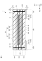
- FIG. 1 is a perspective view showing a multilayer ceramic capacitor according to the present embodiment.
- FIG. 2 is a cross-sectional view (LT cross-section) taken along line II-II of the multilayer ceramic capacitor shown in FIG. 1.
- FIG. 2 is a cross-sectional view (WT cross-section) taken along line III-III of the multilayer ceramic capacitor shown in FIG. 1.
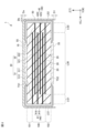
- FIG. 3 is a perspective view showing a multilayer ceramic capacitor according to a modification of the present embodiment.
- 5 is a cross-sectional view (LT cross-section) taken along the line V-V of the multilayer ceramic capacitor shown in FIG. 4.
- FIG. 5 is a cross-sectional view (WT cross-section) taken along the line VI-VI of the multilayer ceramic capacitor shown in FIG. 4.
- FIG. 3 is a perspective view showing a multilayer ceramic capacitor according to a modification of the present embodiment.
- 8 is a cross-sectional view (LT cross-section) of the multilayer ceramic capacitor shown in FIG. 7 taken along line VIII-VIII.
- 8 is a cross-sectional view (WT cross-section) taken along line IX-IX of the multilayer ceramic capacitor shown in FIG. 7.
- FIG. 11 is a perspective view showing a multilayer ceramic capacitor according to a modified example of the present embodiment.
- FIG. 3 is a perspective view showing a multilayer ceramic capacitor according to a modification of the present embodiment.
- FIG. 3 is a perspective view showing a multilayer ceramic capacitor according to a modification of the present embodiment.
- FIG. 1 is a perspective view showing the multilayer ceramic capacitor according to the present embodiment
- FIG. 2 is a sectional view taken along the line II-II of the multilayer ceramic capacitor shown in FIG. 1
- FIG. 3 is a perspective view showing the multilayer ceramic capacitor shown in FIG. FIG. 3 is a sectional view taken along the line III-III of the capacitor.
- a multilayer ceramic capacitor 1 shown in FIGS. 1 to 3 includes a multilayer body 10, an external electrode 40, and a stress suppressing film 50.
- External electrode 40 includes a first external electrode 41 and a second external electrode 42 .
- FIGS. 1 to 3 An XYZ orthogonal coordinate system is shown in FIGS. 1 to 3 and the drawings described below.
- the X direction is the length direction L of the multilayer ceramic capacitor 1 and the laminate 10
- the Y direction is the width direction W of the multilayer ceramic capacitor 1 and the laminate 10
- the Z direction is the length direction L of the multilayer ceramic capacitor 1 and the laminate 10.
- the direction is T. Accordingly, the cross section shown in FIG. 2 is also referred to as the LT cross section, and the cross section shown in FIG. 3 is also referred to as the WT cross section.
- the length direction L, the width direction W, and the lamination direction T are not necessarily orthogonal to each other, but may be intersecting with each other.
- the laminate 10 has a substantially rectangular parallelepiped shape, and has a first main surface TS1 and a second main surface TS2 facing in the stacking direction T, and a first side surface WS1 and a second side surface WS2 facing in the width direction W. , has a first end surface LS1 and a second end surface LS2 facing each other in the length direction L.
- a corner is a part where three sides of the laminate 10 intersect, and a ridgeline is a part where two sides of the laminate 10 intersect.
- the stacked body 10 includes a plurality of dielectric layers 20 and a plurality of internal electrode layers 30 stacked in the stacking direction T. Further, in the stacking direction T, the stacked body 10 includes an inner layer section 100, and a first outer layer section 101 and a second outer layer section 102 that are arranged to sandwich the inner layer section 100.
- the inner layer section 100 includes a portion of the plurality of dielectric layers 20 and the plurality of internal electrode layers 30. In the inner layer section 100, a plurality of internal electrode layers 30 are arranged facing each other with the dielectric layer 20 in between.
- the inner layer portion 100 is a portion that generates capacitance and essentially functions as a capacitor.
- the first outer layer part 101 is arranged on the first main surface TS1 side of the laminate 10, and the second outer layer part 102 is arranged on the second main surface TS2 side of the laminate 10. More specifically, the first outer layer portion 101 is arranged between the internal electrode layer 30 closest to the first main surface TS1 among the plurality of internal electrode layers 30 and the first main surface TS1. , the second outer layer portion 102 is arranged between the internal electrode layer 30 closest to the second main surface TS2 among the plurality of internal electrode layers 30 and the second main surface TS2.
- the first outer layer section 101 and the second outer layer section 102 do not include the internal electrode layer 30 and each include a portion of the plurality of dielectric layers 20 other than a portion for the inner layer section 100.
- the first outer layer section 101 and the second outer layer section 102 are portions that function as a protective layer of the inner layer section 100.
- dielectric layer 20 As a material for the dielectric layer 20, for example, a dielectric ceramic containing BaTiO 3 , CaTiO 3 , SrTiO 3 , CaZrO 3 or the like as a main component can be used. Further, as the material of the dielectric layer 20, a Mn compound, an Fe compound, a Cr compound, a Co compound, a Ni compound, or the like may be added as a subcomponent. More specifically, dielectric layer 20 includes a plurality of dielectric grains. The dielectric grain is a barium titanate ceramic such as a perovskite compound containing Ba and Ti. The dielectric grains may contain at least one of La, Ce, Pr, Nd, Sm, Eu, Gd, Tb, Dy, Ho, Er, Tm, Yb, Lu, and Y as a subcomponent.
- the thickness of the dielectric layer 20 is not particularly limited, but may be, for example, 0.30 ⁇ m or more and 5.0 ⁇ m or less.
- the number of dielectric layers 20 is not particularly limited, but may be, for example, 5 or more and 2000 or less. Note that the number of dielectric layers 20 is the total number of dielectric layers in the inner layer portion and the number of dielectric layers in the outer layer portion.
- the plurality of internal electrode layers 30 include a plurality of first internal electrode layers 31 and a plurality of second internal electrode layers 32.
- the plurality of first internal electrode layers 31 and the plurality of second internal electrode layers 32 are arranged alternately in the stacking direction T of the stacked body 10.
- the first internal electrode layer 31 includes a counter electrode section 311 and an extraction electrode section 312, and the second internal electrode layer 32 includes a counter electrode section 321 and an extraction electrode section 322.
- the counter electrode section 311 and the counter electrode section 321 are opposed to each other in the stacking direction T of the stacked body 10 with the dielectric layer 20 interposed therebetween.
- the shapes of the counter electrode section 311 and the counter electrode section 321 are not particularly limited, and may be, for example, approximately rectangular.
- the counter electrode portion 311 and the counter electrode portion 321 are portions (effective regions) that generate capacitance and essentially function as a capacitor.
- the extraction electrode section 312 extends from the counter electrode section 311 toward the first end surface LS1 of the laminate 10, and is exposed at the first end surface LS1.
- the extraction electrode section 322 extends from the counter electrode section 321 toward the second end surface LS2 of the stacked body 10, and is exposed at the second end surface LS2.
- the shapes of the extraction electrode portion 312 and the extraction electrode portion 322 are not particularly limited, and may be approximately rectangular, for example.
- the first internal electrode layer 31 is connected to the first external electrode 41, and the first internal electrode layer 31 and the second end surface LS2 of the laminate 10, that is, the second external electrode 42, are connected to each other. A gap exists between them.
- the second internal electrode layer 32 is connected to the second external electrode 42, and between the second internal electrode layer 32 and the first end surface LS1 of the laminate 10, that is, the first external electrode 41. There is a gap.
- the first internal electrode layer 31 and the second internal electrode layer 32 contain metal Ni as a main component. Further, the first internal electrode layer 31 and the second internal electrode layer 32 are made of, for example, a metal such as Cu, Ag, Pd, or Au, or an alloy containing at least one of these metals, such as an Ag-Pd alloy. , may be included as a main component, or may be included as a component other than the main component. Furthermore, the first internal electrode layer 31 and the second internal electrode layer 32 may contain dielectric particles having the same composition as the ceramic contained in the dielectric layer 20 as a component other than the main component. In this specification, the main component metal is defined as the metal component having the highest weight percentage.
- the thickness of the first internal electrode layer 31 and the second internal electrode layer 32 is not particularly limited, but may be, for example, 0.30 ⁇ m or more and 1.0 ⁇ m or less.
- the number of first internal electrode layers 31 and second internal electrode layers 32 is not particularly limited, but may be, for example, 5 or more and 2000 or less.
- the laminate 10 includes, in the width direction W, an electrode facing part W30 where the internal electrode layer 30 faces, a first side gap part WG1 and a first side gap part WG1 arranged to sandwich the electrode facing part W30. 2 side gap portions WG2.
- the first side gap portion WG1 is located between the electrode facing portion W30 and the first side surface WS1
- the second side gap portion WG2 is located between the electrode facing portion W30 and the second side surface WS2. do.
- first side gap portion WG1 is located between the end of the internal electrode layer 30 on the first side surface WS1 side and the first side surface WS1
- second side gap portion WG2 is It is located between the end of the internal electrode layer 30 on the second side surface WS2 side and the second side surface WS2.
- the first side gap portion WG1 and the second side gap portion WG2 do not include the internal electrode layer 30 but only include the dielectric layer 20.
- the first side gap portion WG1 and the second side gap portion WG2 are portions that function as a protective layer for the internal electrode layer 30. Note that the first side gap portion WG1 and the second side gap portion WG2 are also referred to as a W gap.
- the laminate 10 has, in the length direction L, an electrode facing portion L30 where the first internal electrode layer 31 and the second internal electrode layer 32 of the internal electrode layer 30 face each other, a first end gap portion LG1, and a second end gap portion LG2.
- the first end gap portion LG1 is located between the electrode facing portion L30 and the first end face LS1
- the second end gap portion LG2 is located between the electrode facing portion L30 and the second end face LS2. More specifically, the first end gap portion LG1 is located between the end of the second internal electrode layer 32 on the first end face LS1 side and the first end face LS1
- the second end gap portion LG2 is located between the end of the first internal electrode layer 31 on the second end face LS2 side and the second end face LS2.
- the first end gap LG1 does not include the second internal electrode layer 32, but includes the first internal electrode layer 31 and the dielectric layer 20, and the second end gap LG2 does not include the first internal electrode layer 31, but includes the second internal electrode layer 32 and the dielectric layer 20.
- the first end gap LG1 is a portion that functions as an extraction electrode portion to the first end surface LS1 of the first internal electrode layer 31, and the second end gap LG2 is a portion that functions as an extraction electrode portion to the second end surface LS2 of the second internal electrode layer 32.
- the first end gap LG1 and the second end gap LG2 are also referred to as L gaps.
- the counter electrode section 311 of the first internal electrode layer 31 and the counter electrode section 321 of the second internal electrode layer 32 described above are located in the electrode opposing section L30. Furthermore, the extraction electrode portion 312 of the first internal electrode layer 31 described above is located in the first end gap portion LG1, and the extraction electrode portion 312 of the aforementioned second internal electrode layer 32 is located in the second end gap portion LG2. An extraction electrode section 322 is located there.
- the dimensions of the above-mentioned laminate 10 are not particularly limited, but for example, the length in the length direction L is 0.05 mm or more and 1.00 mm or less, and the width in the width direction W is 0.10 mm or more and 0.50 mm or less. , the thickness in the stacking direction T may be 0.10 mm or more and 0.50 mm or less. Further, the dimensions of the multilayer ceramic capacitor 1 including the external electrodes 40 described below are not particularly limited, but for example, the length in the length direction L is 0.05 mm or more and 1.00 mm or less, and the width in the width direction W is 0.05 mm or more. The thickness may be 10 mm or more and 0.50 mm or less, and the thickness in the lamination direction T may be 0.10 mm or more and 0.50 mm or less.
- a method for measuring the thickness of the dielectric layer 20 and the internal electrode layer 30 includes, for example, a method of observing the LT cross section of the laminate exposed by polishing near the center in the width direction using a scanning electron microscope. Further, each value may be an average value of measured values at a plurality of locations in the length direction, or may be an average value of measured values at a plurality of locations in the lamination direction.
- the LT cross section near the center in the width direction of the laminate exposed by polishing or the thickness of the laminate exposed by polishing or An example of this method is to observe the WT cross section near the longitudinal center of the multilayer ceramic capacitor using a scanning electron microscope. Further, each value may be an average value of measured values at a plurality of locations in the length direction or width direction.
- the LT cross section of the laminate or multilayer ceramic capacitor exposed by polishing near the center in the width direction is measured using a scanning electron microscope.
- the observation method is the observation method.
- each value may be an average value of measured values at a plurality of locations in the stacking direction.
- the WT cross section near the longitudinal center of the laminate or multilayer ceramic capacitor exposed by polishing is observed using a scanning electron microscope. One method is to do so.
- each value may be an average value of measured values at a plurality of locations in the stacking direction.
- the external electrode 40 includes a first external electrode 41 and a second external electrode 42.
- the first external electrode 41 is arranged on at least the second main surface TS2 of the laminate 10, specifically, on a part of the second main surface TS2 on the first end surface LS1 side.
- the first external electrode 41 is also arranged on the first end surface LS1 of the stacked body 10, and is connected to the first internal electrode layer 31. That is, the first external electrode 41 is L-shaped in the LT cross section, and is arranged along a part of the second main surface TS2 of the laminate 10 on the first end surface LS1 side and the first end surface LS1. ing. Note that in the examples shown in FIGS. 1 to 3, the first external electrode 41 is not arranged on the first main surface TS1 and the two side surfaces WS1 and WS2.
- the second external electrode 42 is arranged on at least the second main surface TS2 of the laminate 10, specifically, on a part of the second main surface TS2 on the second end surface LS2 side.
- the second external electrode 42 is also arranged on the second end surface LS2 of the stacked body 10, and is connected to the second internal electrode layer 32. That is, the second external electrode 42 has an L-shape and is arranged along a part of the second main surface TS2 of the stacked body 10 on the second end surface LS2 side and along the second end surface LS2.
- the second external electrode 42 is not arranged on the first main surface TS1 and the two side surfaces WS1 and WS2.
- the first external electrode 41 has a first base electrode layer 415 and a first plating layer 416
- the second external electrode 42 has a second base electrode layer 425 and a second plating layer 426. has. Note that the first external electrode 41 may be composed only of the first plating layer 416, and the second external electrode 42 may be composed only of the second plating layer 426.
- the first base electrode layer 415 and the second base electrode layer 425 may be fired layers containing metal and glass.
- the glass include glass components containing at least one selected from B, Si, Ba, Mg, Al, Li, and the like. As a specific example, borosilicate glass can be used.
- the metal includes Cu as a main component. Further, the metal may include at least one selected from Ni, Ag, Pd, or Au, or an alloy such as Ag-Pd alloy as a main component, or may contain as a component other than the main component. But that's fine.
- the fired layer is a layer obtained by applying a conductive paste containing metal and glass to the laminate using a dipping method and firing it. Note that the firing may be performed after the internal electrode layer is fired, or the firing may be performed simultaneously with the internal electrode layer. Moreover, the fired layer may be a plurality of layers.
- the first base electrode layer 415 and the second base electrode layer 425 may be resin layers containing conductive particles and a thermosetting resin.
- the resin layer may be formed on the above-mentioned fired layer, or may be formed directly on the laminate without forming the fired layer.
- the resin layer is a layer obtained by applying a conductive paste containing conductive particles and a thermosetting resin to the laminate using a coating method and then baking it. Note that the firing may be performed after the internal electrode layer is fired, or the firing may be performed simultaneously with the internal electrode layer. Moreover, the resin layer may be a plurality of layers.
- each of the first base electrode layer 415 and the second base electrode layer 425 as a fired layer or resin layer is not particularly limited, and may be 1 ⁇ m or more and 10 ⁇ m or less.
- the first base electrode layer 415 and the second base electrode layer 425 may be formed by a thin film forming method such as a sputtering method or a vapor deposition method, and may be a thin film layer with a thickness of 1 ⁇ m or less on which metal particles are deposited.
- the first plating layer 416 covers at least a portion of the first base electrode layer 415, and the second plating layer 426 covers at least a portion of the second base electrode layer 425.
- the first plating layer 416 and the second plating layer 426 include, for example, at least one selected from metals such as Cu, Ni, Ag, Pd, or Au, or alloys such as an Ag-Pd alloy.
- Each of the first plating layer 416 and the second plating layer 426 may be formed of multiple layers. Preferably, it has a two-layer structure of Ni plating and Sn plating.
- the Ni plating layer can prevent the base electrode layer from being eroded by solder when mounting ceramic electronic components, and the Sn plating layer can improve the wettability of solder when mounting ceramic electronic components. , can be easily implemented.
- each of the first plating layer 416 and the second plating layer 426 is not particularly limited, and may be 1 ⁇ m or more and 10 ⁇ m or less.
- the stress suppression film 50 suppresses stress applied to the laminate 10 and the external electrode 40.
- the stress suppression film 50 extends along the first main surface (upper surface) TS1 and the two end surfaces LS1, LS2 so as to cover the laminate 10 and the external electrode 40, and also extends along the first main surface TS1 and the two side surfaces WS1, WS2.
- the end of the stress suppressing film 50 protrudes by D1 from the outermost surface (the surface located closest to the bottom) of the external electrode 40 on the second main surface (bottom surface, mounting surface) TS2 side.
- the protrusion dimension D1 of the end portion of the stress suppressing film 50 may be 5 ⁇ m or more and 10 ⁇ m or less. When D1 is 5 ⁇ m or more, a stress suppressing effect can be obtained, and when D1 is 10 ⁇ m or less, connectivity between the external electrode 40 and the paste solder can be obtained.
- the film thickness Da of the main surface portion (first portion) along the first main surface TS1 and the film thickness Db of the side portion (second portion) along the two end faces LS1, LS2 and the two side faces WS1, WS2 satisfy the following relational expression: 0.8 Da ⁇ Db
- the thickness Da of the main surface portion (first portion) may be 4.5 ⁇ m or more and 5.5 ⁇ m or less.
- the film thickness Da of the main surface portion (first portion) is relatively thick, the adsorption force applied to the upper first main surface TS1 side when adsorbed by the mounter is reduced to the first main surface of the stress suppressing film 50.
- the main surface portion along TS1 can receive it, and the adsorption force applied to the laminate 10 can be suppressed.
- the film thickness Db of the side surface portion (second portion) is relatively thin, the solder pads on the mounting board can be made small, and high-density packaging becomes possible.
- the stress suppressing film 50 is made of an insulating material. Thereby, short circuiting of the external electrode 40 can be prevented.
- the strength of the stress suppression film 50 is preferably higher than the strength of the plurality of dielectric layers 20 of the laminate 10. Specifically, in terms of strength against stress during mounting using a mounter, it is preferable that the strength of the stress suppression film 50 is higher than the strength of the plurality of dielectric layers 20 of the laminate 10.
- the Young's modulus of the stress suppressing film 50 is preferably 400 GPa or more and 1500 GPa or less.
- examples of the material for the stress suppressing film 50 include diamond-like carbon, glass, and the like. Among these, diamond-like carbon is preferable as the material for the stress suppressing film 50.
- a method for manufacturing the above-described multilayer ceramic capacitor 1 will be explained.
- a dielectric sheet for the dielectric layer 20 and a conductive paste for the internal electrode layer 30 are prepared.
- the dielectric sheet and conductive paste contain a binder and a solvent. Known materials can be used as the binder and solvent.
- an internal electrode pattern is formed on the dielectric sheet by printing a conductive paste in a predetermined pattern, for example, on the dielectric sheet.
- a method for forming the internal electrode pattern screen printing, gravure printing, or the like can be used.
- a predetermined number of dielectric sheets for the second outer layer portion 102 on which internal electrode patterns are not printed are laminated.
- dielectric sheets for the inner layer portion 100 on which internal electrode patterns are printed are sequentially laminated.
- a predetermined number of dielectric sheets for the first outer layer portion 101 on which internal electrode patterns are not printed are laminated thereon. In this way, a laminated sheet is produced.
- the laminated sheet is pressed in the lamination direction by means such as a hydrostatic press to produce a laminated block.
- the laminated block is cut to a predetermined size, and laminated chips are cut out.
- dielectric sheets for the first side margin portion W11 and the second side margin portion W12 may be attached to the side surface of the laminated chip.
- the corners and ridges of the laminated chips are rounded by barrel polishing or the like.
- the stacked chips are fired to produce the stacked body 10.
- the firing temperature is preferably 900° C. or more and 1400° C. or less, although it depends on the materials of the dielectric and internal electrodes.
- a conductive paste which is an electrode material for the base electrode layer (for the first base electrode layer 415), is applied to the second main surface TS2 and the first end surface LS1 of the laminate 10 using a coating method.
- a conductive paste which is an electrode material for the base electrode layer (for the second base electrode layer 425) is applied to the second main surface TS2 and the second end surface LS2 of the laminate 10 using a coating method. do.
- first base electrode layer 415 and second base electrode layer 425 which are fired layers, are formed.
- the firing temperature is preferably 600°C or higher and 900°C or lower.
- first base electrode layer 415 and the second base electrode layer 425 which are thin films, may be formed by a thin film forming method such as a sputtering method or a vapor deposition method.
- the base electrode layer was formed and fired after the laminated chip was fired, that is, the laminated body and the external electrode were fired separately.
- the base electrode layer may be formed and fired before firing the laminated chip, that is, the laminated body and the external electrodes may be fired at the same time.
- a first plating layer 416 is formed on the surface of the first base electrode layer 415 to form the first external electrode 41, and a second plating layer 426 is formed on the surface of the second base electrode layer 425. Then, the second external electrode 42 is formed.
- a stress suppressing film 50 is formed to cover the stacked body 10 and the external electrodes 40.
- the method for forming the stress suppressing film 50 include a PVD (Physical Vapor Deposition) method such as a sputtering method, a vapor deposition method, and the like.
- the protrusion dimension D1 of the stress suppressing film 50 can be adjusted by adjusting the height of the mounting jig. Note that the shapes of the protruding portions in FIG. 1 and FIGS. 4, 7, and 10 to 12, which will be described later, may be modified by a mounting jig.
- stress is applied to the first main surface TS1, which is the top surface of the multilayer ceramic capacitor, and this causes the external stress on the second main surface TS2, which is the bottom surface (mounting surface) of the multilayer ceramic capacitor.
- Stress is applied to the electrode 40, which may cause damage to the multilayer ceramic capacitor.
- cracks may occur in the ceramic layer (dielectric layer 20) of the laminate 10. If a crack that occurs in the ceramic layer (dielectric layer 20) extends to the internal electrode layer 30, for example, moisture will enter the crack and the insulation of the multilayer ceramic capacitor will deteriorate.
- the stress suppression film 50 extends along the first main surface (top surface) TS1 and the two end surfaces LS1, LS2 so as to cover the laminate 10 and the external electrode 40, and also extends along the first main surface (top surface) TS1 and the two side surfaces WS1, WS2, and the end of the stress suppression film 50 protrudes by D1 from the outermost surface (surface located closest to the bottom) of the external electrode 40 on the second main surface (bottom surface, mounting surface) TS2 side.
- the stress applied to the first main surface TS1 side which is the top surface
- the stress applied to the first main surface TS1 side can be dispersed from the main surface portion along the first main surface TS1 of the stress suppression film 50 to the end surface portions along the two end surfaces LS1, LS2 and the side surface portions along the two side surfaces WS1, WS2, and can be released to the protruding end.
- This makes it possible to suppress the stress applied to the external electrode 40 on the second main surface TS2, which is the bottom surface (mounting surface), and to the laminate 10, and to suppress the occurrence of cracks in the ceramic layer (dielectric layer 20) of the laminate 10.
- the multilayer ceramic capacitor 1 of this embodiment even when the capacitor is made thin, it is possible to suppress a decrease in strength against external stress.
- the adsorption force applied to the first main surface TS1 side which is the upper surface, is also applied to the main surface along the first main surface TS1 of the stress suppressing film 50.
- the surface part can be received.
- the adsorption force applied to the laminate 10 can also be suppressed.
- the stress suppressing film 50 covers the external electrodes 40 on the end surfaces LS1, LS2 or the side surfaces WS1, WS2, so that paste solder does not spread on the end surfaces LS1, LS2 or the side surfaces WS1, WS2. It is possible to prevent it from rising. This makes it possible to reduce the size of the solder pads on the mounting board, allowing for high-density packaging.
- the external electrode 40 is not formed on the first main surface TS1 side, the number of laminated layers in the multilayer body 10 can be increased, and the effective area of the capacitor can be increased. Can be done. Further, since the external electrode 40 is not formed on the two side surfaces WS1 and WS2, the area in the stacked body 10 can be increased, and the effective area of the capacitor can be increased.
- the stress suppressing film 50 extends along five surfaces: the first main surface (upper surface) TS1, the two end surfaces LS1, LS2, and the two side surfaces WS1, WS2. .
- the present invention is not limited thereto, and the stress suppressing film 50 may extend along only three surfaces, the first main surface (upper surface) TS1 and the two end surfaces LS1 and LS2.
- the stress suppressing film 50 may extend along only three surfaces, the first main surface (upper surface) TS1 and the two side surfaces WS1 and WS2.
- the two external electrodes 40 are arranged on a part of the two end surfaces LS1, LS2 side of the second main surface TS2 of the laminate 10 and on the two end surfaces LS1, LS2. did.
- the shape, number, and arrangement position of the external electrodes 40 are not limited thereto.
- the present invention is also applicable to a configuration in which a plurality of external electrodes 40 are arranged on at least a part of the second main surface TS2 of the stacked body 10.
- the present invention is also applicable to a configuration in which the plurality of external electrodes 40 are arranged at least on a part of the two side surfaces WS1 and WS2 of the second main surface TS2.
- some examples of the shape, number, and arrangement position of the external electrodes 40 will be shown.
- FIG. 5 is a cross-sectional view taken along the VV line of the multilayer ceramic capacitor shown in FIG.
- FIG. 3 is a cross-sectional view taken along the line VI-VI of a ceramic capacitor.
- the multilayer ceramic capacitor 1 shown in FIGS. 4 to 6 has a different shape of the external electrode 40 compared to the multilayer ceramic capacitor 1 shown in FIGS. 1 to 3.
- the first external electrode 41 is arranged only on the second main surface (bottom surface, mounting surface) TS2 of the laminate 10, specifically, on a part of the second main surface TS2 on the first end surface LS1 side. ing. That is, the first external electrode 41 is not arranged on the first end surface LS1, the first main surface (upper surface) TS1, the first side surface WS1, and the second side surface WS2. In this case, for example, the first external electrode 41 and the first internal electrode layer 31 are connected by one or more vias 35 extending in the stacking direction T on the first end surface LS1 side of the stacked body 10. Bye.
- the second external electrode 42 is arranged only on the second main surface (bottom surface, mounting surface) TS2 of the laminate 10, specifically, on a part of the second main surface TS2 on the second end surface LS2 side. ing. That is, the second external electrode 42 is not arranged on the second end surface LS2, the first main surface (upper surface) TS1, the first side surface WS1, and the second side surface WS2. In this case, for example, the second external electrode 42 and the second internal electrode layer 32 are connected by one or more vias 35 extending in the stacking direction T on the second end surface LS2 side of the stacked body 10. Bye.
- the method for forming the vias 35 is not limited, but for example, after the above-described laminated block is manufactured and before the laminated chip is cut out, a plurality of holes arranged in the width direction are formed near the end of the laminated chip, The formed holes may be filled with conductive paste.
- (Modification 2) 7 is a perspective view showing a multilayer ceramic capacitor according to a modification of the present embodiment
- FIG. 8 is a sectional view taken along line VIII-VIII of the multilayer ceramic capacitor shown in FIG. 7
- FIG. FIG. 3 is a sectional view taken along the line IX-IX of the multilayer ceramic capacitor shown in FIG.
- the multilayer ceramic capacitor 1 shown in FIGS. 7 to 9 has a different shape of the external electrode 40 compared to the multilayer ceramic capacitor 1 shown in FIGS. 1 to 3.
- the first external electrode 41 is disposed on a part of the second main surface (bottom surface, mounting surface) TS2 of the laminate 10 on the first end surface LS1 side and on the first end surface LS1. It is connected to the internal electrode layer 31 of. Furthermore, in the examples shown in FIGS. 7 to 9, the first external electrode 41 is also arranged in a part of the first main surface (upper surface) TS1 of the laminate 10 on the first end surface LS1 side, and It is also arranged in a part of the first end surface LS1 side of the first side surface WS1 of the body 10, and also arranged in a part of the second end surface LS1 side of the second side surface WS2 of the stacked body 10. .
- the first external electrode 41 has a U-shape (Angular U-shape) in the LT cross section, and includes a portion of the second main surface TS2 of the laminate 10 on the first end surface LS1 side, the first end surface LS1 and along a portion of the first main surface TS1 on the first end surface LS1 side. Further, the first external electrode 41 has a U-shape (Angular U-shape) in the LW cross section, and includes a part of the first end surface LS1 side of the first side surface WS1 of the laminate 10, and a portion of the first end surface LS1 , and along a part of the second side surface WS2 on the first end surface LS1 side.
- Angular U-shape Angular U-shape
- the second external electrode 42 is disposed on a part of the second main surface (bottom surface, mounting surface) TS2 of the laminate 10 on the second end surface LS2 side and on the second end surface LS2. is connected to the internal electrode layer 32 of.
- the second external electrode 42 is also arranged in a part of the first main surface (upper surface) TS1 of the laminate 10 on the second end surface LS2 side, and It is also arranged in a part of the first side surface WS1 of the body 10 on the second end surface LS2 side, and also in a part of the second end surface LS2 side of the second side surface WS2 of the stacked body 10. .
- the second external electrode 42 has a U-shape (Angular U-shape) in the LT cross section, and includes a part of the second main surface TS2 of the laminate 10 on the second end surface LS2 side, and a second end surface. LS2 and along a portion of the first main surface TS1 on the second end surface LS2 side.
- the second external electrode 42 has a U-shape (Angular U-shape) in the LW cross section, and includes a part of the first side surface WS1 of the laminate 10 on the second end surface LS2 side, and a portion of the second end surface LS2 , and along a part of the second side surface WS2 on the second end surface LS2 side.
- a flat spacer member 55 may be disposed on each of the first main surface TS1 and the second main surface TS2 in a portion where the multiple external electrodes 40 are not disposed.
- the stress suppression film 50 may extend on the first main surface TS1 so as to cover the spacer member 55. This can suppress the step between the portion where the external electrodes 40 are disposed and the portion where the external electrodes 40 are not disposed on the first main surface TS1, which is the upper surface, and can improve the adhesion by the mounter. Note that, since there is no distinction between the upper and lower surfaces in the form before the stress suppression film 50 is formed, it is preferable that the spacer member 55 is disposed on both the first main surface TS1 and the second main surface TS2.
- FIG. 10 is a perspective view showing a multilayer ceramic capacitor according to a modification of this embodiment.
- the multilayer ceramic capacitor 1 shown in FIG. 10 differs in the number of external electrodes 40 from the multilayer ceramic capacitor 1 shown in FIGS. 7 to 9.
- the external electrode 40 includes a third external electrode 43 and a fourth external electrode in addition to the first external electrode 41 and the second external electrode 42. 44 included.
- the multilayer ceramic capacitor 1 includes the third external electrode 43 and the fourth external electrode 44 in addition to the first external electrode 41 and the second external electrode 42.
- the features of the present invention can also be applied to such a three-terminal multilayer ceramic capacitor.
- the third external electrode 43 is located between the first external electrode 41 and the second external electrode 42 on the first side surface WS1 side of the second main surface (bottom surface, mounting surface) TS2 of the laminate 10. A portion thereof is disposed on the first side surface WS1. Further, in the example of FIG. 10, the third external electrode 43 is also arranged on a part of the first main surface (top surface) TS1 of the stacked body 10 on the first side surface WS1 side.
- the third external electrode 43 has a U-shape (Angular U-shape) in the WT cross section, and includes a portion of the second main surface TS2 of the laminate 10 on the first side surface WS1 side, WS1 and along a part of the first main surface TS1 on the first side surface WS1 side.
- U-shape Angular U-shape
- the fourth external electrode 44 is located between the first external electrode 41 and the second external electrode 42 on the second side surface WS2 side of the second main surface (bottom surface, mounting surface) TS2 of the laminate 10. A portion thereof is disposed on the second side surface WS2. In the example of FIG. 10, the fourth external electrode 44 is also arranged on a part of the first main surface (top surface) TS1 of the stacked body 10 on the second side surface WS2 side.
- the fourth external electrode 44 has a U-shape (Angular U-shape) in the WT cross section, and includes a portion of the second main surface TS2 of the laminate 10 on the second side surface WS2 side, a second side surface It is arranged along WS2 and a part of the second side surface WS2 side of the first main surface TS1.
- U-shape Angular U-shape
- a plurality of external electrodes 40 are arranged on each of the first main surface TS1 and the second main surface TS2, similarly to the multilayer ceramic capacitor 1 shown in FIGS. 7 to 9.
- a flat plate-shaped spacer member 55 may be arranged in the portion where the spacer member 55 is not covered. In this case, the stress suppressing film 50 only needs to extend so as to further cover the spacer member 55 on the first main surface TS1.
- the external electrode 40 has an angular U-shape in cross section as an example of the shape of the external electrode 40.
- the features of the present invention are not limited to this, and in the multilayer ceramic capacitor 1 shown in FIG. 10, the multilayer ceramic capacitor 1 shown in FIG. It is also applicable to the multilayer ceramic capacitor 1.
- the third external electrode 43 is L-shaped in the WT cross section, and is arranged along a part of the second main surface TS2 of the stacked body 10 on the first side surface WS1 side and the first side surface WS1. be done.
- the fourth external electrode 44 has an L-shape in the WT cross section, and is arranged along a part of the second main surface TS2 of the laminate 10 on the second side surface WS2 side and the second side surface WS2. Ru.
- the present invention is characterized in that, in the multilayer ceramic capacitor 1 shown in FIG. It is also applicable to capacitor 1.
- FIG. 11 is a perspective view showing a multilayer ceramic capacitor according to a modification of this embodiment.
- the multilayer ceramic capacitor 1 shown in FIG. 11 differs from the multilayer ceramic capacitor 1 shown in FIGS. 7 to 9 in the number and arrangement positions of external electrodes 40.
- the external electrode 40 includes a first external electrode 41, a second external electrode 42, a third external electrode 43, and a fourth external electrode at four corners of the laminate 10 when viewed from the second main surface TS2 side.
- Such a multilayer ceramic capacitor 1 includes two multilayer ceramic capacitors, for example, between the first external electrode 41 and the second external electrode 42 and between the third external electrode 43 and the fourth external electrode 44. Ceramic capacitor elements can be included. The features of the present invention can also be applied to such multi-terminal multilayer ceramic capacitors.
- the first external electrode 41 is provided at the corners of the second main surface (bottom surface, mounting surface) TS2 of the laminate 10 on the first end surface LS1 side and the first side surface WS1 side, and on the first end surface LS1. and a portion of the first side surface WS1. In the example of FIG. 11, the first external electrode 41 is also arranged at the corner of the first main surface (top surface) TS1 of the laminate 10 on the first end surface LS1 side and the first side surface WS1 side. ing.
- the first external electrode 41 has a U-shape (Angular U-shape) in the LT cross section, and includes a portion of the second main surface TS2 of the laminate 10 on the first end surface LS1 side, the first end surface It is arranged along LS1 and a part of the first end surface LS1 side of the first main surface TS1.
- the first external electrode 41 has a U-shape (Angular U-shape) in the WT cross section, and includes a part of the second main surface TS2 of the laminate 10 on the first side surface WS1 side, the first side surface WS1 and along a part of the first main surface TS1 on the first side surface WS1 side.
- the second external electrode 42 is provided at the corners of the second main surface (bottom surface, mounting surface) TS2 of the laminate 10 on the second end surface LS2 side and the first side surface WS1 side, and on the second end surface LS2. and a portion of the first side surface WS1.
- the second external electrode 42 is also arranged at the corner of the first main surface (top surface) TS1 of the laminate 10 on the second end surface LS2 side and on the first side surface WS1 side. ing.
- the second external electrode 42 has a U-shape (Angular U-shape) in the LT cross section, and includes a portion of the second main surface TS2 of the laminate 10 on the second end surface LS2 side, and a second end surface. LS2 and along a portion of the first main surface TS1 on the second end surface LS2 side. Further, the second external electrode 42 has a U-shape (Angular U-shape) in the WT cross section, and includes a part of the second main surface TS2 of the laminate 10 on the first side surface WS1 side, WS1 and along a part of the first main surface TS1 on the first side surface WS1 side.
- Angular U-shape Angular U-shape
- the third external electrode 43 is provided at the corners of the second main surface (bottom surface, mounting surface) TS2 of the laminate 10 on the first end surface LS1 side and the second side surface WS2 side, and on the first end surface LS1. and a portion of the second side surface WS2.
- the third external electrode 43 is also arranged at the corner of the first main surface (upper surface) TS1 of the stacked body 10 on the first end surface LS1 side and on the second side surface WS2 side. ing.
- the third external electrode 43 has a U-shape (Angular U-shape) in the LT cross section, and includes a portion of the second main surface TS2 of the laminate 10 on the first end surface LS1 side, the first end surface It is arranged along LS1 and a part of the first end surface LS1 side of the first main surface TS1.
- the third external electrode 43 has a U-shape (Angular U-shape) in the WT cross section, and includes a portion of the second main surface TS2 of the laminate 10 on the second side surface WS2 side, a portion of the second side surface WS2 side, It is arranged along WS2 and a part of the second side surface WS2 side of the first main surface TS1.
- the fourth external electrode 44 is provided at the corners of the second main surface (bottom surface, mounting surface) TS2 of the laminate 10 on the second end surface LS2 side and the second side surface WS2 side, and on the second end surface LS2. and a portion of the second side surface WS2. In the example of FIG. 11, the fourth external electrode 44 is also arranged at the corner of the first main surface (upper surface) TS1 of the laminate 10 on the second end surface LS2 side and the second side surface WS2 side. ing.
- the fourth external electrode 44 has a U-shape (Angular U-shape) in the LT cross section, and includes a portion of the second main surface TS2 of the laminate 10 on the second end surface LS2 side, and a portion of the second end surface TS2 of the laminate 10. LS2 and along a portion of the first main surface TS1 on the second end surface LS2 side.
- U-shape Angular U-shape
- the fourth external electrode 44 has a U-shape (Angular U-shape) in the WT cross section, and includes a portion of the second main surface TS2 of the laminate 10 on the second side surface WS2 side, a portion of the second side surface WS2 side, It is arranged along WS2 and a part of the second side surface WS2 side of the first main surface TS1.
- U-shape Angular U-shape
- a plurality of external electrodes 40 are arranged on each of the first main surface TS1 and the second main surface TS2, similarly to the multilayer ceramic capacitor 1 shown in FIGS. 7 to 9.
- a flat plate-shaped spacer member 55 may be arranged in the portion where the spacer member 55 is not covered. In this case, the stress suppressing film 50 only needs to extend so as to further cover the spacer member 55 on the first main surface TS1.
- the external electrode 40 has an angular U-shape in cross section as an example of the shape of the external electrode 40.
- the features of the present invention are not limited to this, and in the multilayer ceramic capacitor 1 shown in FIG. 10, the multilayer ceramic capacitor 1 shown in FIG. It is also applicable to the multilayer ceramic capacitor 1.
- the first external electrode 41 is L-shaped in the LT cross section, and is arranged along a part of the second main surface TS2 of the laminate 10 on the first end surface LS1 side and the first end surface LS1.
- the second external electrode 42 is L-shaped in the LT cross section, and is arranged along a part of the second main surface TS2 of the laminate 10 on the second end surface LS2 side and the second end surface LS2. , and has an L-shape in the WT cross section, and is arranged along a part of the second main surface TS2 of the laminate 10 on the first side surface WS1 side and along the first side surface WS1.
- the third external electrode 43 has an L-shape in the LT cross section, and is arranged along a part of the second main surface TS2 of the laminate 10 on the first end surface LS1 side and the first end surface LS1. , and has an L-shape in the WT cross section, and is arranged along a part of the second main surface TS2 of the laminate 10 on the second side surface WS2 side and along the second side surface WS2.
- the fourth external electrode 44 is L-shaped in the LT cross section, and is arranged along a part of the second main surface TS2 of the laminate 10 on the second end surface LS2 side and along the second end surface LS2. , and has an L-shape in the WT cross section, and is arranged along a part of the second main surface TS2 of the laminate 10 on the second side surface WS2 side and along the second side surface WS2.
- a feature of the present invention is that in the multilayer ceramic capacitor 1 shown in FIG. It is also applicable to capacitor 1.
- Fig. 12 is a perspective view showing a multilayer ceramic capacitor according to a modified example of this embodiment.
- the multilayer ceramic capacitor 1 shown in Fig. 12 differs from the multilayer ceramic capacitor 1 shown in Figs. 7 to 9 in the number and arrangement positions of the external electrodes 40.
- the external electrode 40 includes a first external electrode 41, a third external electrode 43, a fifth external electrode 45, and a seventh external electrode 47 on the first side surface WS1 side of the multilayer body 10.
- 10 includes a second external electrode 42, a fourth external electrode 44, a sixth external electrode 46, and an eighth external electrode 48 on the second side surface WS2 side.
- Such a multilayer ceramic capacitor 1 includes, for example, between the first external electrode 41 and the second external electrode 42, between the third external electrode 43 and the fourth external electrode 44, and between the fifth external electrode
- Four multilayer ceramic capacitor elements can be arranged in an array between 45 and the sixth external electrode 46 and between the seventh external electrode 47 and the eighth external electrode 48.
- the features of the present invention can also be applied to such an array type multilayer ceramic capacitor.
- Each of the first external electrode 41, the third external electrode 43, the fifth external electrode 45, and the seventh external electrode 47 is connected to the first external electrode on the second main surface (bottom surface, mounting surface) TS2 of the laminate 10. and on the first side surface WS1. Further, in the example of FIG. 12, each of the first external electrode 41, the third external electrode 43, the fifth external electrode 45, and the seventh external electrode 47 ) It is also arranged on a part of the first side surface WS1 side of TS1. That is, each of the first external electrode 41, the third external electrode 43, the fifth external electrode 45, and the seventh external electrode 47 has a U-shape (Angular U-shape) in the WT cross section, and is a laminate. 10 second main surface TS2 on the first side surface WS1 side, the first side surface WS1, and a part of the first main surface TS1 on the first side surface WS1 side. .
- U-shape Angular U-shape
- the second external electrode 42, the fourth external electrode 44, the sixth external electrode 46, and the eighth external electrode 48 are located on the second side surface of the second main surface (bottom surface, mounting surface) TS2 of the laminate 10. It is arranged on a part of the WS2 side and on the second side surface WS2. In the example of FIG. 12, the second external electrode 42, the fourth external electrode 44, the sixth external electrode 46, and the eighth external electrode 48 are connected to the first main surface (top surface) TS1 of the stacked body 10. It is also arranged on a part of the second side surface WS2 side.
- the second external electrode 42 , the fourth external electrode 44 , the sixth external electrode 46 , and the eighth external electrode 48 have a U-shape (Angular U-shape) in the WT cross section, and They are arranged along a part of the second main surface TS2 on the second side surface WS2 side, the second side surface WS2, and a part of the first main surface TS1 on the second side surface WS2 side.
- U-shape Angular U-shape
- a plurality of external electrodes 40 are arranged on each of the first main surface TS1 and the second main surface TS2, similarly to the multilayer ceramic capacitor 1 shown in FIGS. 7 to 9.
- a flat plate-shaped spacer member 55 may be arranged in the portion where the spacer member 55 is not covered. In this case, the stress suppressing film 50 only needs to extend so as to further cover the spacer member 55 on the first main surface TS1.
- the external electrode 40 has an angular U-shape in cross section as an example of the shape of the external electrode 40.
- the features of the present invention are not limited thereto, and in the multilayer ceramic capacitor 1 shown in FIG. 12, the multilayer ceramic capacitor 1 shown in FIG. It is also applicable to the multilayer ceramic capacitor 1.
- each of the first external electrode 41, the third external electrode 43, the fifth external electrode 45, and the seventh external electrode 47 is L-shaped in the WT cross section, and It is arranged along a part of the main surface TS2 on the first side surface WS1 side and along the first side surface WS1.
- the second external electrode 42, the fourth external electrode 44, the sixth external electrode 46, and the eighth external electrode 48 are L-shaped in the WT cross section, and the second main surface TS2 of the laminate 10 and along the second side surface WS2.
- a feature of the present invention is that in the multilayer ceramic capacitor 1 shown in FIG. It is also applicable to capacitor 1.
- the stress suppressing film 50 extends along five surfaces: the first main surface (upper surface) TS1, the two end surfaces LS1, TS2, and the two side surfaces WS1, WS2. did.
- the present invention is not limited thereto, and the stress suppressing film 50 may have a form extending along three surfaces, the first main surface (upper surface) TS1 and the two end surfaces LS1 and LS2.
- the stress suppressing film 50 may extend along three surfaces: the first main surface (top surface) TS1 and the two side surfaces WS1 and WS2.
- the present invention may have the following forms. ⁇ 1> A laminate in which a plurality of dielectric layers made of a ceramic material and a plurality of internal electrode layers are stacked, a first main surface and a second main surface facing in the stacking direction, and a first main surface and a second main surface facing in the stacking direction.
- a laminate having two side faces facing each other in a width direction intersecting with the stacking direction and two end faces facing each other in a length direction crossing the stacking direction and the width direction; a plurality of external electrodes arranged on at least the second main surface of the laminate; a stress suppression film that suppresses stress applied to the laminate and the plurality of external electrodes; Equipped with The stress suppressing film is It is made of insulating material, Extending along the first main surface and the two end surfaces so as to cover the laminate and the plurality of external electrodes, or extending along the first main surface and the two side surfaces. It extends, An end portion of the stress suppressing film protrudes from the outermost surface of the plurality of external electrodes on the second main surface side. Multilayer ceramic capacitor.
- the stress suppression film extends along the first main surface and the two end surfaces, and extends along the first main surface and the two side surfaces.
- ⁇ 3> The multilayer ceramic capacitor according to ⁇ 1> or ⁇ 2>, wherein the stress suppression film has a strength higher than that of the plurality of dielectric layers of the laminate.
- ⁇ 4> The multilayer ceramic capacitor according to any one of ⁇ 1> to ⁇ 3>, wherein the stress suppression film has a Young's modulus of 400 GPa or more and 1500 GPa or less.
- ⁇ 5> The multilayer ceramic capacitor according to any one of ⁇ 1> to ⁇ 4>, wherein the stress suppressing film contains diamond-like carbon or glass as a material.
- the film thickness Da of the first portion along the first main surface and the film thickness Db of the second portion along the two end faces or the two side faces are as follows.
- Each of the plurality of external electrodes is It is L-shaped in a cross section along the stacking direction and the length direction, and is arranged along one of the second main surface and the two end surfaces of the laminate, or It is L-shaped in a cross section along the stacking direction and the width direction, and is arranged along the second main surface and one of the two side surfaces of the laminate.
- the multilayer ceramic capacitor according to any one of ⁇ 1> to ⁇ 7>.
- Each of the plurality of external electrodes is arranged only along the second main surface of the laminate,
- the laminate has a plurality of vias extending in the stacking direction and connecting the plurality of external electrode layers and different parts of the plurality of internal electrode layers, respectively.
- the multilayer ceramic capacitor according to any one of ⁇ 1> to ⁇ 7>.
- Each of the plurality of external electrodes A cross section along the stacking direction and the length direction is U-shaped, and is disposed along the second main surface, one of the two end surfaces, and the first main surface of the laminate, or a U-shaped cross section along the stacking direction and the width direction, and disposed along the second main surface, one of the two side surfaces, and the first main surface of the laminate; a flat spacer member is disposed on each of the first main surface and the second main surface in a portion where the plurality of external electrodes are not disposed, the stress suppression film extends on the first main surface so as to further cover the spacer member; ⁇ 8> The multilayer ceramic capacitor according to any one of ⁇ 1> to ⁇ 7>.
- Multilayer ceramic capacitor 10 Laminated body 20 Dielectric layer 30 Internal electrode layer 31 First internal electrode layer 311 First counter electrode section 312 First extraction electrode section 32 Second internal electrode layer 321 Second counter electrode section 322 Second extraction electrode section 35 Via 40 External electrode 41 First external electrode 415 First base electrode layer 416 First plating layer 42 Second external electrode 425 Second base electrode layer 426 Second plating layer 50 Stress suppression film 55 Spacer member 100 Inner layer part 101 First outer layer part 102 Second outer layer part L30 Electrode facing part LG1 First end gap part LG2 Second end gap part W30 Electrode facing part WG1 First side gap Part WG2 Second side gap L Length direction T Lamination direction W Width direction LS1 First end surface LS2 Second end surface TS1 First main surface TS2 Second main surface WS1 First side surface WS2 Second side surface
Landscapes
- Engineering & Computer Science (AREA)
- Power Engineering (AREA)
- Manufacturing & Machinery (AREA)
- Microelectronics & Electronic Packaging (AREA)
- Fixed Capacitors And Capacitor Manufacturing Machines (AREA)
- Ceramic Capacitors (AREA)
Abstract
薄型化を図っても、外部応力に対する強度の低下を抑制することができる積層セラミックコンデンサを提供する。積層セラミックコンデンサ1は、セラミック材料からなる複数の誘電体層20と複数の内部電極層30とが積層された積層体10と、積層体10の少なくとも第2の主面TS2に配置された複数の外部電極40と、積層体10および複数の外部電極40にかかる応力を抑制する応力抑制膜50とを備える。応力抑制膜50は、絶縁性を有する材料で構成されており、積層体10および複数の外部電極40を覆うように、第1の主面TS1および2つの端面LS1,LS2に沿って延在しており、または、第1の主面TS1および2つの側面に沿って延在している。応力抑制膜50の端部は、第2の主面TS2側において、複数の外部電極40の最外面よりも突出している。
Description
本発明は、積層セラミックコンデンサに関する。
セラミック材料からなる複数の誘電体層と複数の内部電極層とが積層された積層体と、積層体の端面または側面に配置された外部電極とを備えた積層セラミックコンデンサが知られている。このような積層セラミックコンデンサにおいて、更なる小型化、薄型化が求められている(例えば、特許文献1参照)。
積層セラミックコンデンサが薄膜化されると、積層体、特にセラミック層、の強度が低下し、実装時のマウンタからの応力によって積層セラミックコンデンサにダメージが生じることがある。例えば、積層体のセラミック層にクラックが生じることがある。セラミック層に生じるクラックが内部電極層まで進展してしまうと、例えばクラックに水分が浸入し、積層セラミックコンデンサの絶縁性が低下してしまう。
本発明は、薄型化を図っても、外部応力に対する強度の低下を抑制することができる積層セラミックコンデンサを提供することを目的とする。
本発明に係る積層セラミックコンデンサは、セラミック材料からなる複数の誘電体層と複数の内部電極層とが積層された積層体であって、積層方向に相対する第1の主面および第2の主面と、前記積層方向に交差する幅方向に相対する2つの側面と、前記積層方向および前記幅方向に交差する長さ方向に相対する2つの端面とを有した積層体と、前記積層体の少なくとも前記第2の主面に配置された複数の外部電極と、前記積層体および前記複数の外部電極にかかる応力を抑制する応力抑制膜とを備える。前記応力抑制膜は、絶縁性を有する材料で構成されており、前記積層体および前記複数の外部電極を覆うように、前記第1の主面および前記2つの端面に沿って延在しており、または、前記第1の主面および前記2つの側面に沿って延在している。前記応力抑制膜の端部は、前記第2の主面側において、前記複数の外部電極の最外面よりも突出している。
本発明によれば、積層セラミックコンデンサにおいて、薄型化を図っても、外部応力に対する強度の低下を抑制することができる。
以下、添付の図面を参照して本発明の実施形態の一例について説明する。なお、各図面において同一または相当の部分に対しては同一の符号を附すこととする。
<積層セラミックコンデンサ>
図1は、本実施形態に係る積層セラミックコンデンサを示す斜視図であり、図2は、図1に示す積層セラミックコンデンサのII-II線断面図であり、図3は、図1に示す積層セラミックコンデンサのIII-III線断面図である。図1~図3に示す積層セラミックコンデンサ1は、積層体10と、外部電極40と、応力抑制膜50とを備える。外部電極40は、第1の外部電極41と第2の外部電極42とを含む。
図1は、本実施形態に係る積層セラミックコンデンサを示す斜視図であり、図2は、図1に示す積層セラミックコンデンサのII-II線断面図であり、図3は、図1に示す積層セラミックコンデンサのIII-III線断面図である。図1~図3に示す積層セラミックコンデンサ1は、積層体10と、外部電極40と、応力抑制膜50とを備える。外部電極40は、第1の外部電極41と第2の外部電極42とを含む。
図1~図3および後述する図面には、XYZ直交座標系が示されている。X方向は積層セラミックコンデンサ1および積層体10の長さ方向Lであり、Y方向は積層セラミックコンデンサ1および積層体10の幅方向Wであり、Z方向は積層セラミックコンデンサ1および積層体10の積層方向Tである。これにより、図2に示す断面はLT断面とも称され、図3に示す断面はWT断面とも称される。
なお、長さ方向L、幅方向Wおよび積層方向Tは、必ずしも互いに直交する関係になるとは限らず、互いに交差する関係であってもよい。
積層体10は、略直方体形状であり、積層方向Tに相対する第1の主面TS1および第2の主面TS2と、幅方向Wに相対する第1の側面WS1および第2の側面WS2と、長さ方向Lに相対する第1の端面LS1および第2の端面LS2とを有する。
積層体10の角部および稜線部には、丸みがつけられていると好ましい。角部は、積層体10の3面が交る部分であり、稜線部は、積層体10の2面が交る部分である。
図2および図3に示すように、積層体10は、積層方向Tに積層された複数の誘電体層20と複数の内部電極層30とを有する。また、積層体10は、積層方向Tにおいて、内層部100と、内層部100を挟み込むように配置された第1の外層部101および第2の外層部102とを有する。
内層部100は、複数の誘電体層20の一部と複数の内部電極層30とを含む。内層部100では、複数の内部電極層30が誘電体層20を介して対向して配置されている。内層部100は、静電容量を発生させ実質的にコンデンサとして機能する部分である。
第1の外層部101は、積層体10の第1の主面TS1側に配置されており、第2の外層部102は、積層体10の第2の主面TS2側に配置されている。より具体的には、第1の外層部101は、複数の内部電極層30のうち第1の主面TS1に最も近い内部電極層30と第1の主面TS1との間に配置されており、第2の外層部102は、複数の内部電極層30のうち第2の主面TS2に最も近い内部電極層30と第2の主面TS2との間に配置されている。第1の外層部101および第2の外層部102は、内部電極層30を含まず、複数の誘電体層20のうち内層部100のための一部以外の部分をそれぞれ含む。第1の外層部101および第2の外層部102は、内層部100の保護層として機能する部分である。
誘電体層20の材料としては、例えば、BaTiO3、CaTiO3、SrTiO3、またはCaZrO3等を主成分として含む誘電体セラミックを用いることができる。また、誘電体層20の材料としては、Mn化合物、Fe化合物、Cr化合物、Co化合物、またはNi化合物等を副成分として添加されてもよい。
より具体的には、誘電体層20は、複数の誘電体グレインを含む。誘電体グレインは、Ba、Tiを含むペロブスカイト型化合物などのチタン酸バリウム系セラミックである。誘電体グレインは、La、Ce、Pr、Nd、Sm、Eu、Gd、Tb、Dy、Ho、Er、Tm、Yb、LuおよびYのうち少なくとも1種を副成分として含んでいてもよい。
より具体的には、誘電体層20は、複数の誘電体グレインを含む。誘電体グレインは、Ba、Tiを含むペロブスカイト型化合物などのチタン酸バリウム系セラミックである。誘電体グレインは、La、Ce、Pr、Nd、Sm、Eu、Gd、Tb、Dy、Ho、Er、Tm、Yb、LuおよびYのうち少なくとも1種を副成分として含んでいてもよい。
誘電体層20の厚さは、特に限定されないが、例えば0.30μm以上5.0μm以下であってもよい。誘電体層20の枚数は、特に限定されないが、例えば5枚以上2000枚以下であってもよい。なお、この誘電体層20の枚数は、内層部の誘電体層の枚数と外層部の誘電体層の枚数との総数である。
図2および図3に示すように、複数の内部電極層30は、複数の第1の内部電極層31および複数の第2の内部電極層32を含む。複数の第1の内部電極層31および複数の第2の内部電極層32は、積層体10の積層方向Tに交互に配置されている。
第1の内部電極層31は、対向電極部311と引出電極部312とを含み、第2の内部電極層32は、対向電極部321と引出電極部322とを含む。
対向電極部311と対向電極部321とは、積層体10の積層方向Tにおいて誘電体層20を介して互いに対向している。対向電極部311および対向電極部321の形状は、特に限定されず、例えば略矩形状であればよい。対向電極部311と対向電極部321とは、静電容量を発生させ実質的にコンデンサとして機能する部分(有効領域)である。
引出電極部312は、対向電極部311から積層体10の第1の端面LS1に向けて延在し、第1の端面LS1において露出している。引出電極部322は、対向電極部321から積層体10の第2の端面LS2に向けて延在し、第2の端面LS2において露出している。引出電極部312および引出電極部322の形状は、特に限定されず、例えば略矩形状であればよい。
これにより、第1の内部電極層31は第1の外部電極41に接続され、第1の内部電極層31と、積層体10の第2の端面LS2、すなわち第2の外部電極42、との間にはギャップが存在する。また、第2の内部電極層32は第2の外部電極42に接続され、第2の内部電極層32と、積層体10の第1の端面LS1、すなわち第1の外部電極41、との間にはギャップが存在する。
第1の内部電極層31および第2の内部電極層32は、金属Niを主成分として含む。また、第1の内部電極層31および第2の内部電極層32は、例えば、Cu、Ag、Pd、またはAu等の金属、またはAg-Pd合金等の、それらの金属の少なくとも一種を含む合金、から選ばれる少なくとも1つを主成分として含んでもよいし、主成分以外の成分として含んでもよい。更に、第1の内部電極層31および第2の内部電極層32は、誘電体層20に含まれるセラミックと同一組成系の誘電体の粒子を主成分以外の成分として含んでいてもよい。なお、本明細書において、主成分の金属とは、最も重量%が高い金属成分であると定める。
第1の内部電極層31および第2の内部電極層32の厚さは、特に限定されないが、例えば0.30μm以上1.0μm以下であってもよい。第1の内部電極層31および第2の内部電極層32の枚数は、特に限定されないが、例えば5枚以上2000枚以下であってもよい。
図3に示すように、積層体10は、幅方向Wにおいて、内部電極層30が対向する電極対向部W30と、電極対向部W30を挟み込むように配置された第1のサイドギャップ部WG1および第2のサイドギャップ部WG2とを有する。第1のサイドギャップ部WG1は、電極対向部W30と第1の側面WS1との間に位置し、第2のサイドギャップ部WG2は、電極対向部W30と第2の側面WS2との間に位置する。より具体的には、第1のサイドギャップ部WG1は、内部電極層30の第1の側面WS1側の端と第1の側面WS1との間に位置し、第2のサイドギャップ部WG2は、内部電極層30の第2の側面WS2側の端と第2の側面WS2との間に位置する。第1のサイドギャップ部WG1および第2のサイドギャップ部WG2は、内部電極層30を含まず、誘電体層20のみを含む。第1のサイドギャップ部WG1および第2のサイドギャップ部WG2は、内部電極層30の保護層として機能する部分である。なお、第1のサイドギャップ部WG1および第2のサイドギャップ部WG2は、Wギャップともいう。
図2に示すように、積層体10は、長さ方向Lにおいて、内部電極層30の第1の内部電極層31と第2の内部電極層32とが対向する電極対向部L30と、第1のエンドギャップ部LG1と、第2のエンドギャップ部LG2とを有する。第1のエンドギャップ部LG1は、電極対向部L30と第1の端面LS1との間に位置し、第2のエンドギャップ部LG2は、電極対向部L30と第2の端面LS2との間に位置する。より具体的には、第1のエンドギャップ部LG1は、第2の内部電極層32の第1の端面LS1側の端と第1の端面LS1との間に位置し、第2のエンドギャップ部LG2は、第1の内部電極層31の第2の端面LS2側の端と第2の端面LS2との間に位置する。第1のエンドギャップ部LG1は、第2の内部電極層32を含まず、第1の内部電極層31および誘電体層20を含み、第2のエンドギャップ部LG2は、第1の内部電極層31を含まず、第2の内部電極層32および誘電体層20を含む。第1のエンドギャップ部LG1は、第1の内部電極層31の第1の端面LS1への引出電極部として機能する部分であり、第2のエンドギャップ部LG2は、第2の内部電極層32の第2の端面LS2への引出電極部として機能する部分である。第1のエンドギャップ部LG1および第2のエンドギャップ部LG2は、Lギャップともいう。
なお、電極対向部L30には、上述した第1の内部電極層31の対向電極部311および第2の内部電極層32の対向電極部321が位置する。また、第1のエンドギャップ部LG1には、上述した第1の内部電極層31の引出電極部312が位置し、第2のエンドギャップ部LG2には、上述した第2の内部電極層32の引出電極部322が位置する。
上述した積層体10の寸法は、特に限定されないが、例えば長さ方向Lの長さが0.05mm以上1.00mm以下であり、幅方向Wの幅が0.10mm以上0.50mm以下であり、積層方向Tの厚さが0.10mm以上0.50mm以下であってもよい。
また、後述する外部電極40を含む積層セラミックコンデンサ1の寸法は、特に限定されないが、例えば長さ方向Lの長さが0.05mm以上1.00mm以下であり、幅方向Wの幅が0.10mm以上0.50mm以下であり、積層方向Tの厚さが0.10mm以上0.50mm以下であってもよい。
また、後述する外部電極40を含む積層セラミックコンデンサ1の寸法は、特に限定されないが、例えば長さ方向Lの長さが0.05mm以上1.00mm以下であり、幅方向Wの幅が0.10mm以上0.50mm以下であり、積層方向Tの厚さが0.10mm以上0.50mm以下であってもよい。
なお、誘電体層20および内部電極層30の厚さの測定方法としては、例えば研磨により露出させた積層体の幅方向中央近傍のLT断面を走査型電子顕微鏡にて観察する方法が挙げられる。また、各値は、長さ方向の複数個所の測定値の平均値であってもよいし、更に積層方向の複数個所の測定値の平均値であってもよい。
同様に、積層体10の厚さまたは積層セラミックコンデンサ1の厚さの測定方法としては、例えば研磨により露出させた積層体の幅方向中央近傍のLT断面、または、研磨により露出させた積層体または積層セラミックコンデンサの長さ方向中央近傍のWT断面を走査型電子顕微鏡にて観察する方法が挙げられる。また、各値は、長さ方向または幅方向の複数個所の測定値の平均値であってもよい。
同様に、積層体10の長さまたは積層セラミックコンデンサ1の長さの測定方法としては、例えば研磨により露出させた積層体または積層セラミックコンデンサの幅方向中央近傍のLT断面を走査型電子顕微鏡にて観察する方法が挙げられる。また、各値は、積層方向の複数個所の測定値の平均値であってもよい。
同様に、積層体10の幅または積層セラミックコンデンサ1の幅の測定方法としては、例えば研磨により露出させた積層体または積層セラミックコンデンサの長さ方向中央近傍のWT断面を走査型電子顕微鏡にて観察する方法が挙げられる。また、各値は、積層方向の複数個所の測定値の平均値であってもよい。
同様に、積層体10の長さまたは積層セラミックコンデンサ1の長さの測定方法としては、例えば研磨により露出させた積層体または積層セラミックコンデンサの幅方向中央近傍のLT断面を走査型電子顕微鏡にて観察する方法が挙げられる。また、各値は、積層方向の複数個所の測定値の平均値であってもよい。
同様に、積層体10の幅または積層セラミックコンデンサ1の幅の測定方法としては、例えば研磨により露出させた積層体または積層セラミックコンデンサの長さ方向中央近傍のWT断面を走査型電子顕微鏡にて観察する方法が挙げられる。また、各値は、積層方向の複数個所の測定値の平均値であってもよい。
外部電極40は、第1の外部電極41と第2の外部電極42とを含む。
第1の外部電極41は、積層体10の少なくとも第2の主面TS2、具体的には第2の主面TS2における第1の端面LS1側の一部、に配置されている。図1~図3の例では、第1の外部電極41は、積層体10の第1の端面LS1にも配置されており、第1の内部電極層31に接続されている。すなわち、第1の外部電極41は、LT断面においてL字形状であり、積層体10の第2の主面TS2の第1の端面LS1側の一部および第1の端面LS1に沿って配置されている。なお、図1~図3の例では、第1の外部電極41は、第1の主面TS1および2つの側面WS1,WS2には配置されていない。
第2の外部電極42は、積層体10の少なくとも第2の主面TS2、具体的には第2の主面TS2における第2の端面LS2側の一部、に配置されている。図1~図3の例では、第2の外部電極42は、積層体10の第2の端面LS2にも配置されており、第2の内部電極層32に接続されている。すなわち、第2の外部電極42は、L字形状であり、積層体10の第2の主面TS2の第2の端面LS2側の一部および第2の端面LS2に沿って配置されている。なお、図1~図3の例では、第2の外部電極42は、第1の主面TS1および2つの側面WS1,WS2には配置されていない。
第1の外部電極41は、第1の下地電極層415と第1のめっき層416とを有し、第2の外部電極42は、第2の下地電極層425と第2のめっき層426とを有する。なお、第1の外部電極41は第1のめっき層416のみから構成されていてもよいし、第2の外部電極42は第2のめっき層426のみから構成されていてもよい。
第1の下地電極層415および第2の下地電極層425は、金属とガラスとを含む焼成層であってもよい。ガラスとしては、B、Si、Ba、Mg、Al、またはLi等から選ばれる少なくとも1つを含むガラス成分が挙げられる。具体例として、ホウケイ酸ガラスを用いることができる。金属としては、Cuを主成分として含む。また、金属としては、例えばNi、Ag、Pd、またはAu等の金属、またはAg-Pd合金等の合金、から選ばれる少なくとも1つを主成分として含んでもよいし、主成分以外の成分として含んでもよい。
焼成層は、金属およびガラスを含む導電性ペーストをディップ法によって積層体に塗布して焼成した層である。なお、内部電極層の焼成後に焼成されてもよく、内部電極層と同時に焼成されてもよい。また、焼成層は、複数層であってもよい。
或いは、第1の下地電極層415および第2の下地電極層425は、導電性粒子と熱硬化性樹脂とを含む樹脂層であってもよい。樹脂層は、上述した焼成層上に形成されてもよいし、焼成層を形成せずに積層体に直接形成されてもよい。
樹脂層は、導電性粒子と熱硬化性樹脂とを含む導電性ペーストを塗布法によって積層体に塗布して焼成した層である。なお、内部電極層の焼成後に焼成されてもよく、内部電極層と同時に焼成されてもよい。また、樹脂層は、複数層であってもよい。
焼成層または樹脂層としての第1の下地電極層415および第2の下地電極層425の各々の一層あたりの厚さとしては、特に限定されず、1μm以上10μm以下であってもよい。
或いは、第1の下地電極層415および第2の下地電極層425は、スパッタ法または蒸着法等の薄膜形成法により形成され、金属粒子が堆積された1μm以下の薄膜層であってもよい。
第1のめっき層416は、第1の下地電極層415の少なくとも一部を覆い、第2のめっき層426は、第2の下地電極層425の少なくとも一部を覆う。第1のめっき層416および第2のめっき層426としては、例えば、Cu、Ni、Ag、Pd、またはAu等の金属、またはAg-Pd合金等の合金から選ばれる少なくとも1つを含む。
第1のめっき層416および第2のめっき層426の各々は複数層により形成されていてもよい。好ましくは、NiめっきおよびSnめっきの2層構造である。Niめっき層は、下地電極層がセラミック電子部品を実装する際のはんだによって侵食されることを防止することができ、Snめっき層は、セラミック電子部品を実装する際のはんだの濡れ性を向上させ、容易に実装することができる。
第1のめっき層416および第2のめっき層426の各々の一層あたりの厚さとしては、特に限定されず、1μm以上10μm以下であってもよい。
<<応力抑制膜>>
応力抑制膜50は、積層体10および外部電極40にかかる応力を抑制する。応力抑制膜50は、積層体10および外部電極40を覆うように、第1の主面(上面)TS1および2つの端面LS1,LS2に沿って延在しており、かつ、第1の主面TS1および2つの側面WS1,WS2に沿って延在している。
応力抑制膜50は、積層体10および外部電極40にかかる応力を抑制する。応力抑制膜50は、積層体10および外部電極40を覆うように、第1の主面(上面)TS1および2つの端面LS1,LS2に沿って延在しており、かつ、第1の主面TS1および2つの側面WS1,WS2に沿って延在している。
応力抑制膜50の端部は、第2の主面(底面、搭載面)TS2側において、外部電極40の最外面(最も底面側に位置する面)よりもD1だけ突出している。応力抑制膜50の端部の突出寸法D1は、5μm以上10μm以下であればよい。D1が5μm以上であると応力抑制効果が得られ、D1が10μm以下であると外部電極40とペーストはんだとの接続性が得られる。
応力抑制膜50において、第1の主面TS1に沿った主面部分(第1部分)の膜厚Daと、2つの端面LS1,LS2および2つの側面WS1,WS2に沿った側面部分(第2部分)の膜厚Dbとは、以下の関係式を満たす。
0.8Da≧Db
主面部分(第1部分)の膜厚Daは、4.5μm以上5.5μm以下であればよい。
0.8Da≧Db
主面部分(第1部分)の膜厚Daは、4.5μm以上5.5μm以下であればよい。
主面部分(第1部分)の膜厚Daが比較的に厚いと、マウンタによる吸着時、上面となる第1の主面TS1側にかかる吸着力を、応力抑制膜50の第1の主面TS1に沿う主面部分が受けることができ、積層体10にかかる吸着力を抑制することができる。一方、側面部分(第2部分)の膜厚Dbが比較的に薄いと、搭載基板において、はんだパッドを小さくすることができ、高密度実装化が可能となる。
応力抑制膜50は、絶縁性を有する材料で構成されている。これにより、外部電極40の短絡を防止することができる。
応力抑制膜50の強度は、積層体10の複数の誘電体層20の強度よりも高いと好ましい。具体的には、マウンタを用いた実装時の応力に対する強度において、応力抑制膜50の強度は、積層体10の複数の誘電体層20の強度よりも高いと好ましい。例えば、応力抑制膜50のヤング率は、400GPa以上1500GPa以下であると好ましい。
絶縁性および強度の観点で、応力抑制膜50の材料としては、ダイヤモンドライクカーボン、または、ガラス等が挙げられる。これらの中でも、応力抑制膜50の材料としては、ダイヤモンドライクカーボンであると好ましい。
<製造方法>
次に、上述した積層セラミックコンデンサ1の製造方法について説明する。まず、誘電体層20用の誘電体シートおよび内部電極層30用の導電性ペーストを準備する。誘電体シートおよび導電性ペーストには、バインダおよび溶剤が含まれる。バインダおよび溶剤としては公知の材料を用いることができる。
次に、上述した積層セラミックコンデンサ1の製造方法について説明する。まず、誘電体層20用の誘電体シートおよび内部電極層30用の導電性ペーストを準備する。誘電体シートおよび導電性ペーストには、バインダおよび溶剤が含まれる。バインダおよび溶剤としては公知の材料を用いることができる。
次に、誘電体シート上に導電性ペーストを、例えば所定のパターンで印刷することにより、誘電体シート上に内部電極パターンを形成する。内部電極パターンの形成方法としては、スクリーン印刷またはグラビア印刷等を用いることができる。
次に、内部電極パターンが印刷されていない第2の外層部102用の誘電体シートを所定枚数積層する。その上に、内部電極パターンが印刷された内層部100用の誘電体シートを順次積層する。その上に、内部電極パターンが印刷されていない第1の外層部101用の誘電体シートを所定枚数積層する。これにより、積層シートが作製される。
次に、静水圧プレス等の手段により、積層シートを積層方向にプレスし、積層ブロックを作製する。次に、積層ブロックを所定のサイズにカットし、積層チップを切り出す。このとき、積層チップの側面に第1のサイドマージン部W11および第2のサイドマージン部W12用の誘電体シートを貼り付けてもよい。また、このとき、バレル研磨等により積層チップの角部および稜線部に丸みをつける。次に、積層チップを焼成し、積層体10を作製する。焼成温度は、誘電体や内部電極の材料にもよるが、900℃以上1400℃以下であることが好ましい。
次に、塗布法を用いて、積層体10の第2の主面TS2および第1の端面LS1に下地電極層用(第1の下地電極層415用)の電極材料である導電性ペーストを塗布する。同様に、塗布法を用いて、積層体10の第2の主面TS2および第2の端面LS2に下地電極層用(第2の下地電極層425用)の電極材料である導電性ペーストを塗布する。その後、これらの導電性ペーストを焼成することにより、焼成層である第1の下地電極層415および第2の下地電極層425が形成される。焼成温度は、600℃以上900℃以下であることが好ましい。
なお、スパッタ法または蒸着法等の薄膜形成法により、薄膜である第1の下地電極層415および第2の下地電極層425を形成してもよい。
また、上述では、積層チップを焼成した後に下地電極層を形成して焼成した、すなわち積層体と外部電極とを別々に焼成した。しかし、積層チップを焼成する前に下地電極層を形成して焼成してもよい、すなわち、積層体と外部電極とを同時に焼成してもよい。
その後、第1の下地電極層415の表面に第1のめっき層416を形成して第1の外部電極41を形成し、第2の下地電極層425の表面に第2のめっき層426を形成して第2の外部電極42を形成する。
次に、積層体10および外部電極40を覆うように応力抑制膜50を形成する。応力抑制膜50の形成方法としては、スパッタリング法等のPVD法(Physical Vapor Deposition)法、または蒸着法等が挙げられる。このとき、搭載治具の高さを調整することにより、応力抑制膜50の突出寸法D1を調整することができる。なお、図1、および後述する図4、図7および図10~12の突出部分の形状は、搭載治具によって変形されてもよい。
以上の工程により、上述した積層セラミックコンデンサ1が得られる。
以上の工程により、上述した積層セラミックコンデンサ1が得られる。
ここで、応力抑制膜50を備えない従来の積層セラミックコンデンサにおいて、積層セラミックコンデンサが薄膜化されると、積層体10、特にセラミック層(誘電体層20)、の強度が低下し、実装時のマウンタからの応力によって積層セラミックコンデンサにダメージが生じることがある。例えば、マウンタを用いた実装時、積層セラミックコンデンサの上面となる第1の主面TS1側に応力がかかり、これにより、積層セラミックコンデンサの底面(搭載面)となる第2の主面TS2における外部電極40に応力がかかり、積層セラミックコンデンサにダメージが生じることがある。例えば、積層体10のセラミック層(誘電体層20)にクラックが生じることがある。セラミック層(誘電体層20)に生じるクラックが内部電極層30まで進展してしまうと、例えばクラックに水分が浸入し、積層セラミックコンデンサの絶縁性が低下してしまう。
この点に関し、本実施形態の積層セラミックコンデンサ1によれば、応力抑制膜50が、積層体10および外部電極40を覆うように、第1の主面(上面)TS1および2つの端面LS1,LS2に沿って延在しており、かつ、第1の主面(上面)TS1および2つの側面WS1,WS2に沿って延在しており、応力抑制膜50の端部が、第2の主面(底面、搭載面)TS2側において、外部電極40の最外面(最も底面側に位置する面)よりもD1だけ突出している。これにより、マウンタを用いた実装時、上面となる第1の主面TS1側にかかる応力を、応力抑制膜50の第1の主面TS1に沿う主面部分から、2つの端面LS1,LS2に沿う端面部分、および、2つの側面WS1,WS2に沿う側面部分に分散し、突出した端部に逃がすことができる。これにより、底面(搭載面)となる第2の主面TS2における外部電極40、および、積層体10にかかる応力を抑制することができ、積層体10のセラミック層(誘電体層20)にクラックが生じることを抑制することができる。このように、本実施形態の積層セラミックコンデンサ1によれば、薄型化を図っても、外部応力に対する強度の低下を抑制することができる。
また、本実施形態の積層セラミックコンデンサ1によれば、マウンタによる吸着時、上面となる第1の主面TS1側にかかる吸着力をも、応力抑制膜50の第1の主面TS1に沿う主面部分が受けることができる。これにより、積層体10にかかる吸着力をも抑制することができる。
また、本実施形態の積層セラミックコンデンサ1によれば、端面LS1,LS2または側面WS1,WS2における外部電極40を応力抑制膜50が覆うことにより、端面LS1,LS2または側面WS1,WS2にペーストはんだが盛り上がることを防止することができる。これにより、搭載基板において、はんだパッドを小さくすることができ、高密度実装化が可能となる。
また、本実施形態の積層セラミックコンデンサ1によれば、第1の主面TS1側に外部電極40を形成しないので、積層体10における積層数を増加することができ、コンデンサ有効領域を増大することができる。また、2つの側面WS1,WS2側に外部電極40を形成しないので、積層体10における面積を増加することができ、コンデンサ有効領域を増大することができる。
以上、本発明の実施形態について説明したが、本発明は上述した実施形態に限定されることなく、種々の変更および変形が可能である。例えば、上述した実施形態では、応力抑制膜50が、第1の主面(上面)TS1、2つの端面LS1,LS2および2つの側面WS1,WS2の5面に沿って延在する形態を例示した。しかし、本発明はこれに限定されず、応力抑制膜50は、第1の主面(上面)TS1および2つの端面LS1,LS2の3面のみに沿って延在する形態であってもよい。或いは、応力抑制膜50は、第1の主面(上面)TS1および2つの側面WS1,WS2の3面のみに沿って延在する形態であってもよい。
また、上述した実施形態では、2つの外部電極40が、積層体10の第2の主面TS2における2つの端面LS1,LS2側の一部および2つの端面LS1,LS2に配置された形態を例示した。しかし、本発明では、外部電極40の形状、個数および配置位置はこれに限定されない。例えば、本発明は、複数の外部電極40が、積層体10の少なくとも第2の主面TS2の一部に配置された形態にも適用可能である。また、本発明は、複数の外部電極40が、少なくとも第2の主面TS2における2つの側面WS1,WS2側の一部に配置された形態にも適用可能である。以下では、外部電極40の形状、個数および配置位置のいくつかの例を示す。
(変形例1)
図4は、本実施形態の変形例に係る積層セラミックコンデンサを示す斜視図であり、図5は、図4に示す積層セラミックコンデンサのV-V線断面図であり、図6は、図4に示す積層セラミックコンデンサのVI-VI線断面図である。図4~図6に示す積層セラミックコンデンサ1は、図1~図3に示す積層セラミックコンデンサ1と比較して、外部電極40の形状が異なる。
図4は、本実施形態の変形例に係る積層セラミックコンデンサを示す斜視図であり、図5は、図4に示す積層セラミックコンデンサのV-V線断面図であり、図6は、図4に示す積層セラミックコンデンサのVI-VI線断面図である。図4~図6に示す積層セラミックコンデンサ1は、図1~図3に示す積層セラミックコンデンサ1と比較して、外部電極40の形状が異なる。
第1の外部電極41は、積層体10の第2の主面(底面、実装面)TS2、具体的には第2の主面TS2における第1の端面LS1側の一部、のみに配置されている。すなわち、第1の外部電極41は、第1の端面LS1、第1の主面(上面)TS1、第1の側面WS1および第2の側面WS2には配置されていない。この場合、例えば、積層体10の第1の端面LS1側において積層方向Tに延在する1または複数のビア35によって、第1の外部電極41と第1の内部電極層31とが接続されればよい。
第2の外部電極42は、積層体10の第2の主面(底面、実装面)TS2、具体的には第2の主面TS2における第2の端面LS2側の一部、のみに配置されている。すなわち、第2の外部電極42は、第2の端面LS2、第1の主面(上面)TS1、第1の側面WS1および第2の側面WS2には配置されていない。この場合、例えば、積層体10の第2の端面LS2側において積層方向Tに延在する1または複数のビア35によって、第2の外部電極42と第2の内部電極層32とが接続されればよい。
ビア35の形成方法としては、限定されないが、例えば、上述した積層ブロックの作製後であって、積層チップを切り出す前に、積層チップの端部近傍に幅方向に並ぶ複数の孔を形成し、形成した孔に導電性ペーストを充填すればよい。
(変形例2)
図7は、本実施形態の変形例に係る積層セラミックコンデンサを示す斜視図であり、図8は、図7に示す積層セラミックコンデンサのVIII-VIII線断面図であり、図9は、図7に示す積層セラミックコンデンサのIX-IX線断面図である。図7~図9に示す積層セラミックコンデンサ1は、図1~図3に示す積層セラミックコンデンサ1と比較して、外部電極40の形状が異なる。
図7は、本実施形態の変形例に係る積層セラミックコンデンサを示す斜視図であり、図8は、図7に示す積層セラミックコンデンサのVIII-VIII線断面図であり、図9は、図7に示す積層セラミックコンデンサのIX-IX線断面図である。図7~図9に示す積層セラミックコンデンサ1は、図1~図3に示す積層セラミックコンデンサ1と比較して、外部電極40の形状が異なる。
第1の外部電極41は、積層体10の第2の主面(底面、実装面)TS2における第1の端面LS1側の一部、および、第1の端面LS1に配置されており、第1の内部電極層31に接続されている。また、図7~図9の例では、第1の外部電極41は、積層体10の第1の主面(上面)TS1における第1の端面LS1側の一部にも配置されており、積層体10の第1の側面WS1における第1の端面LS1側の一部にも配置されており、積層体10の第2の側面WS2における第1の端面LS1側の一部にも配置されている。すなわち、第1の外部電極41は、LT断面においてU字形状(Angular U-shape)であり、積層体10の第2の主面TS2の第1の端面LS1側の一部、第1の端面LS1、および、第1の主面TS1の第1の端面LS1側の一部に沿って配置されている。また、第1の外部電極41は、LW断面においてU字形状(Angular U-shape)であり、積層体10の第1の側面WS1における第1の端面LS1側の一部、第1の端面LS1、および、第2の側面WS2における第1の端面LS1側の一部に沿って配置されている。
第2の外部電極42は、積層体10の第2の主面(底面、実装面)TS2における第2の端面LS2側の一部、および、第2の端面LS2に配置されており、第2の内部電極層32に接続されている。また、図7~図9の例では、第2の外部電極42は、積層体10の第1の主面(上面)TS1における第2の端面LS2側の一部にも配置されており、積層体10の第1の側面WS1における第2の端面LS2側の一部にも配置されており、積層体10の第2の側面WS2における第2の端面LS2側の一部にも配置されている。すなわち、第2の外部電極42は、LT断面においてU字形状(Angular U-shape)であり、積層体10の第2の主面TS2の第2の端面LS2側の一部、第2の端面LS2、および、第1の主面TS1の第2の端面LS2側の一部に沿って配置されている。また、第2の外部電極42は、LW断面においてU字形状(Angular U-shape)であり、積層体10の第1の側面WS1における第2の端面LS2側の一部、第2の端面LS2、および、第2の側面WS2における第2の端面LS2側の一部に沿って配置されている。
この場合、第1の主面TS1および第2の主面TS2の各々において、複数の外部電極40が配置されていない部分に平板状のスペーサ部材55が配置されていてもよい。この場合、応力抑制膜50は、第1の主面TS1において、更にスペーサ部材55を覆うように延在いていればよい。これにより、上面となる第1の主面TS1において、外部電極40が配置されている部分と外部電極40が配置されていない部分との段差を抑制することができ、マウンタによる吸着性を向上することができる。なお、応力抑制膜50を形成する前の形態では上下面の区別がないため、スペーサ部材55は、第1の主面TS1および第2の主面TS2の両主面に配置されることが好ましい。
(変形例3)
図10は、本実施形態の変形例に係る積層セラミックコンデンサを示す斜視図である。図10に示す積層セラミックコンデンサ1は、図7~図9に示す積層セラミックコンデンサ1と比較して、外部電極40の個数が異なる。
図10は、本実施形態の変形例に係る積層セラミックコンデンサを示す斜視図である。図10に示す積層セラミックコンデンサ1は、図7~図9に示す積層セラミックコンデンサ1と比較して、外部電極40の個数が異なる。
例えば、図7~図9に示す積層セラミックコンデンサ1において、外部電極40は、第1の外部電極41および第2の外部電極42に加えて、更に第3の外部電極43および第4の外部電極44を含む。このように、積層セラミックコンデンサ1は、第1の外部電極41および第2の外部電極42に加えて、3番目の電極である第3の外部電極43および第4の外部電極44を含むことから、3端子型の積層セラミックコンデンサと称される。本発明の特徴は、このような3端子型の積層セラミックコンデンサにも適用可能である。
第3の外部電極43は、第1の外部電極41と第2の外部電極42との間において、積層体10の第2の主面(底面、実装面)TS2における第1の側面WS1側の一部、および、第1の側面WS1に配置されている。また、図10の例では、第3の外部電極43は、積層体10の第1の主面(上面)TS1における第1の側面WS1側の一部にも配置されている。すなわち、第3の外部電極43は、WT断面においてU字形状(Angular U-shape)であり、積層体10の第2の主面TS2における第1の側面WS1側の一部、第1の側面WS1、および、第1の主面TS1における第1の側面WS1側の一部に沿って配置されている。
第4の外部電極44は、第1の外部電極41と第2の外部電極42との間において、積層体10の第2の主面(底面、実装面)TS2における第2の側面WS2側の一部、および、第2の側面WS2に配置されている。また、図10の例では、第4の外部電極44は、積層体10の第1の主面(上面)TS1における第2の側面WS2側の一部にも配置されている。すなわち、第4の外部電極44は、WT断面においてU字形状(Angular U-shape)であり、積層体10の第2の主面TS2における第2の側面WS2側の一部、第2の側面WS2、および、第1の主面TS1における第2の側面WS2側の一部に沿って配置されている。
図10に示す積層セラミックコンデンサ1でも、図7~図9に示す積層セラミックコンデンサ1と同様に、第1の主面TS1および第2の主面TS2の各々において、複数の外部電極40が配置されていない部分に平板状のスペーサ部材55が配置されていてもよい。この場合、応力抑制膜50は、第1の主面TS1において、更にスペーサ部材55を覆うように延在いていればよい。
なお、図10では、外部電極40の形状として断面U字形状(Angular U-shape)の外部電極40を例示した。しかし、本発明の特徴はこれに限定されず、図10に示す積層セラミックコンデンサ1において、図1~図3に示す積層セラミックコンデンサ1と同様に、断面L字形状の外部電極40を備える形態の積層セラミックコンデンサ1にも適用可能である。この場合、第3の外部電極43は、WT断面においてL字形状であり、積層体10の第2の主面TS2における第1の側面WS1側の一部および第1の側面WS1に沿って配置される。また、第4の外部電極44は、WT断面においてL字形状であり、積層体10の第2の主面TS2における第2の側面WS2側の一部および第2の側面WS2に沿って配置される。
また、本発明の特徴は、図10に示す積層セラミックコンデンサ1において、図4~図6に示す積層セラミックコンデンサ1と同様に、第2の主面TS2のみに外部電極40を備える形態の積層セラミックコンデンサ1にも適用可能である。
(変形例4)
図11は、本実施形態の変形例に係る積層セラミックコンデンサを示す斜視図である。図11に示す積層セラミックコンデンサ1は、図7~図9に示す積層セラミックコンデンサ1と比較して、外部電極40の個数および配置位置が異なる。
図11は、本実施形態の変形例に係る積層セラミックコンデンサを示す斜視図である。図11に示す積層セラミックコンデンサ1は、図7~図9に示す積層セラミックコンデンサ1と比較して、外部電極40の個数および配置位置が異なる。
例えば、外部電極40は、第2の主面TS2側からみて積層体10の4つの角部に、第1の外部電極41、第2の外部電極42、第3の外部電極43および第4の外部電極44を含む。このような積層セラミックコンデンサ1は、例えば、第1の外部電極41と第2の外部電極42との間、および、第3の外部電極43と第4の外部電極44との間に2つの積層セラミックコンデンサ素子を含むことができる。本発明の特徴は、このような多端子型の積層セラミックコンデンサにも適用可能である。
第1の外部電極41は、積層体10の第2の主面(底面、実装面)TS2における第1の端面LS1側および第1の側面WS1側の角部、および、第1の端面LS1の一部および第1の側面WS1の一部に配置されている。また、図11の例では、第1の外部電極41は、積層体10の第1の主面(上面)TS1における第1の端面LS1側および第1の側面WS1側の角部にも配置されている。すなわち、第1の外部電極41は、LT断面においてU字形状(Angular U-shape)であり、積層体10の第2の主面TS2における第1の端面LS1側の一部、第1の端面LS1、および、第1の主面TS1における第1の端面LS1側の一部に沿って配置されている。また、第1の外部電極41は、WT断面においてU字形状(Angular U-shape)であり、積層体10の第2の主面TS2における第1の側面WS1側の一部、第1の側面WS1、および、第1の主面TS1における第1の側面WS1側の一部に沿って配置されている。
第2の外部電極42は、積層体10の第2の主面(底面、実装面)TS2における第2の端面LS2側および第1の側面WS1側の角部、および、第2の端面LS2の一部および第1の側面WS1の一部に配置されている。また、図11の例では、第2の外部電極42は、積層体10の第1の主面(上面)TS1における第2の端面LS2側および第1の側面WS1側の角部にも配置されている。すなわち、第2の外部電極42は、LT断面においてU字形状(Angular U-shape)であり、積層体10の第2の主面TS2における第2の端面LS2側の一部、第2の端面LS2、および、第1の主面TS1における第2の端面LS2側の一部に沿って配置されている。また、第2の外部電極42は、WT断面においてU字形状(Angular U-shape)であり、積層体10の第2の主面TS2における第1の側面WS1側の一部、第1の側面WS1、および、第1の主面TS1における第1の側面WS1側の一部に沿って配置されている。
第3の外部電極43は、積層体10の第2の主面(底面、実装面)TS2における第1の端面LS1側および第2の側面WS2側の角部、および、第1の端面LS1の一部および第2の側面WS2の一部に配置されている。また、図11の例では、第3の外部電極43は、積層体10の第1の主面(上面)TS1における第1の端面LS1側および第2の側面WS2側の角部にも配置されている。すなわち、第3の外部電極43は、LT断面においてU字形状(Angular U-shape)であり、積層体10の第2の主面TS2における第1の端面LS1側の一部、第1の端面LS1、および、第1の主面TS1における第1の端面LS1側の一部に沿って配置されている。また、第3の外部電極43は、WT断面においてU字形状(Angular U-shape)であり、積層体10の第2の主面TS2における第2の側面WS2側の一部、第2の側面WS2、および、第1の主面TS1における第2の側面WS2側の一部に沿って配置されている。
第4の外部電極44は、積層体10の第2の主面(底面、実装面)TS2における第2の端面LS2側および第2の側面WS2側の角部、および、第2の端面LS2の一部および第2の側面WS2の一部に配置されている。また、図11の例では、第4の外部電極44は、積層体10の第1の主面(上面)TS1における第2の端面LS2側および第2の側面WS2側の角部にも配置されている。すなわち、第4の外部電極44は、LT断面においてU字形状(Angular U-shape)であり、積層体10の第2の主面TS2における第2の端面LS2側の一部、第2の端面LS2、および、第1の主面TS1における第2の端面LS2側の一部に沿って配置されている。また、第4の外部電極44は、WT断面においてU字形状(Angular U-shape)であり、積層体10の第2の主面TS2における第2の側面WS2側の一部、第2の側面WS2、および、第1の主面TS1における第2の側面WS2側の一部に沿って配置されている。
図11に示す積層セラミックコンデンサ1でも、図7~図9に示す積層セラミックコンデンサ1と同様に、第1の主面TS1および第2の主面TS2の各々において、複数の外部電極40が配置されていない部分に平板状のスペーサ部材55が配置されていてもよい。この場合、応力抑制膜50は、第1の主面TS1において、更にスペーサ部材55を覆うように延在いていればよい。
なお、図11では、外部電極40の形状として断面U字形状(Angular U-shape)の外部電極40を例示した。しかし、本発明の特徴はこれに限定されず、図10に示す積層セラミックコンデンサ1において、図1~図3に示す積層セラミックコンデンサ1と同様に、断面L字形状の外部電極40を備える形態の積層セラミックコンデンサ1にも適用可能である。この場合、第1の外部電極41は、LT断面においてL字形状であり、積層体10の第2の主面TS2における第1の端面LS1側の一部および第1の端面LS1に沿って配置され、かつ、WT断面においてL字形状であり、積層体10の第2の主面TS2における第1の側面WS1側の一部および第1の側面WS1に沿って配置される。また、第2の外部電極42は、LT断面においてL字形状であり、積層体10の第2の主面TS2における第2の端面LS2側の一部および第2の端面LS2に沿って配置され、かつ、WT断面においてL字形状であり、積層体10の第2の主面TS2における第1の側面WS1側の一部および第1の側面WS1に沿って配置される。また、第3の外部電極43は、LT断面においてL字形状であり、積層体10の第2の主面TS2における第1の端面LS1側の一部および第1の端面LS1に沿って配置され、かつ、WT断面においてL字形状であり、積層体10の第2の主面TS2における第2の側面WS2側の一部および第2の側面WS2に沿って配置される。また、第4の外部電極44は、LT断面においてL字形状であり、積層体10の第2の主面TS2における第2の端面LS2側の一部および第2の端面LS2に沿って配置され、かつ、WT断面においてL字形状であり、積層体10の第2の主面TS2における第2の側面WS2側の一部および第2の側面WS2に沿って配置される。
また、本発明の特徴は、図11に示す積層セラミックコンデンサ1において、図4~図6に示す積層セラミックコンデンサ1と同様に、第2の主面TS2のみに外部電極40を備える形態の積層セラミックコンデンサ1にも適用可能である。
(変形例5)
図12は、本実施形態の変形例に係る積層セラミックコンデンサを示す斜視図である。図12に示す積層セラミックコンデンサ1は、図7~図9に示す積層セラミックコンデンサ1と比較して、外部電極40の個数および配置位置が異なる。
図12は、本実施形態の変形例に係る積層セラミックコンデンサを示す斜視図である。図12に示す積層セラミックコンデンサ1は、図7~図9に示す積層セラミックコンデンサ1と比較して、外部電極40の個数および配置位置が異なる。
例えば、外部電極40は、積層体10の第1の側面WS1側に第1の外部電極41、第3の外部電極43、第5の外部電極45および第7の外部電極47を含み、積層体10の第2の側面WS2側に第2の外部電極42、第4の外部電極44、第6の外部電極46および第8の外部電極48を含む。このような積層セラミックコンデンサ1は、例えば、第1の外部電極41と第2の外部電極42との間、第3の外部電極43と第4の外部電極44との間、第5の外部電極45と第6の外部電極46との間、および、第7の外部電極47と第8の外部電極48との間に、4つの積層セラミックコンデンサ素子をアレイ状に配置することができる。本発明の特徴は、このようなアレイ型の積層セラミックコンデンサにも適用可能である。
第1の外部電極41、第3の外部電極43、第5の外部電極45および第7の外部電極47の各々は、積層体10の第2の主面(底面、実装面)TS2における第1の側面WS1側の一部、および、第1の側面WS1に配置されている。また、図12の例では、第1の外部電極41、第3の外部電極43、第5の外部電極45および第7の外部電極47の各々は、積層体10の第1の主面(上面)TS1における第1の側面WS1側の一部にも配置されている。すなわち、第1の外部電極41、第3の外部電極43、第5の外部電極45および第7の外部電極47の各々は、WT断面においてU字形状(Angular U-shape)であり、積層体10の第2の主面TS2における第1の側面WS1側の一部、第1の側面WS1、および、第1の主面TS1における第1の側面WS1側の一部に沿って配置されている。
第2の外部電極42、第4の外部電極44、第6の外部電極46および第8の外部電極48は、積層体10の第2の主面(底面、実装面)TS2における第2の側面WS2側の一部、および、第2の側面WS2に配置されている。また、図12の例では、第2の外部電極42、第4の外部電極44、第6の外部電極46および第8の外部電極48は、積層体10の第1の主面(上面)TS1における第2の側面WS2側の一部にも配置されている。すなわち、第2の外部電極42、第4の外部電極44、第6の外部電極46および第8の外部電極48は、WT断面においてU字形状(Angular U-shape)であり、積層体10の第2の主面TS2における第2の側面WS2側の一部、第2の側面WS2、および、第1の主面TS1における第2の側面WS2側の一部に沿って配置されている。
図12に示す積層セラミックコンデンサ1でも、図7~図9に示す積層セラミックコンデンサ1と同様に、第1の主面TS1および第2の主面TS2の各々において、複数の外部電極40が配置されていない部分に平板状のスペーサ部材55が配置されていてもよい。この場合、応力抑制膜50は、第1の主面TS1において、更にスペーサ部材55を覆うように延在いていればよい。
なお、図12では、外部電極40の形状として断面U字形状(Angular U-shape)の外部電極40を例示した。しかし、本発明の特徴はこれに限定されず、図12に示す積層セラミックコンデンサ1において、図1~図3に示す積層セラミックコンデンサ1と同様に、断面L字形状の外部電極40を備える形態の積層セラミックコンデンサ1にも適用可能である。この場合、第1の外部電極41、第3の外部電極43、第5の外部電極45および第7の外部電極47の各々は、WT断面においてL字形状であり、積層体10の第2の主面TS2における第1の側面WS1側の一部および第1の側面WS1に沿って配置される。また、第2の外部電極42、第4の外部電極44、第6の外部電極46および第8の外部電極48は、WT断面においてL字形状であり、積層体10の第2の主面TS2における第2の側面WS2側の一部および第2の側面WS2に沿って配置される。
また、本発明の特徴は、図12に示す積層セラミックコンデンサ1において、図4~図6に示す積層セラミックコンデンサ1と同様に、第2の主面TS2のみに外部電極40を備える形態の積層セラミックコンデンサ1にも適用可能である。
上述した変形例1~5でも、応力抑制膜50が、第1の主面(上面)TS1、2つの端面LS1,TS2および2つの側面WS1,WS2の5面に沿って延在する形態を例示した。しかし、本発明はこれに限定されず、応力抑制膜50は、第1の主面(上面)TS1および2つの端面LS1,LS2の3面に沿って延在する形態であってもよい。或いは、応力抑制膜50は、第1の主面(上面)TS1および2つの側面WS1,WS2の3面に沿って延在する形態であってもよい。
また、本発明は以下のような形態であってもよい。
<1> セラミック材料からなる複数の誘電体層と複数の内部電極層とが積層された積層体であって、積層方向に相対する第1の主面および第2の主面と、前記積層方向に交差する幅方向に相対する2つの側面と、前記積層方向および前記幅方向に交差する長さ方向に相対する2つの端面とを有した積層体と、
前記積層体の少なくとも前記第2の主面に配置された複数の外部電極と、
前記積層体および前記複数の外部電極にかかる応力を抑制する応力抑制膜と、
を備え、
前記応力抑制膜は、
絶縁性を有する材料で構成されており、
前記積層体および前記複数の外部電極を覆うように、前記第1の主面および前記2つの端面に沿って延在しており、または、前記第1の主面および前記2つの側面に沿って延在しており、
前記応力抑制膜の端部は、前記第2の主面側において、前記複数の外部電極の最外面よりも突出している、
積層セラミックコンデンサ。
<2> 前記応力抑制膜は、前記第1の主面および前記2つの端面に沿って延在しており、かつ、前記第1の主面および前記2つの側面に沿って延在している、<1>に記載の積層セラミックコンデンサ。
<3> 前記応力抑制膜の強度は、前記積層体の前記複数の誘電体層の強度よりも高い、<1>または<2>に記載の積層セラミックコンデンサ。
<4> 前記応力抑制膜のヤング率は、400GPa以上1500GPa以下である、<1>から<3>のいずれかに記載の積層セラミックコンデンサ。
<5> 前記応力抑制膜は、ダイヤモンドライクカーボン、または、ガラスを材料として含む、<1>から<4>のいずれかに記載の積層セラミックコンデンサ。
<6> 前記応力抑制膜において、前記第1の主面に沿った第1部分の膜厚Daと、前記2つの端面または前記2つの側面に沿った第2部分の膜厚Dbとは、以下の関係式を満たす、<1>から<5>のいずれかに記載の積層セラミックコンデンサ。
0.8Da≧Db
0.8Da≧Db
<7> 前記第1部分の膜厚Daは、4.5μm以上5.5μm以下である、<6>に記載の積層セラミックコンデンサ。
<8> 前記複数の外部電極の各々は、
前記積層方向および前記長さ方向に沿う断面においてL字形状であり、前記積層体の前記第2の主面および前記2つの端面の一方に沿って配置されている、または、
前記積層方向および前記幅方向に沿う断面においてL字形状であり、前記積層体の前記第2の主面および前記2つの側面の一方に沿って配置されている、
<1>から<7>のいずれかに記載の積層セラミックコンデンサ。
前記積層方向および前記長さ方向に沿う断面においてL字形状であり、前記積層体の前記第2の主面および前記2つの端面の一方に沿って配置されている、または、
前記積層方向および前記幅方向に沿う断面においてL字形状であり、前記積層体の前記第2の主面および前記2つの側面の一方に沿って配置されている、
<1>から<7>のいずれかに記載の積層セラミックコンデンサ。
<9> 前記複数の外部電極の各々は、前記積層体の前記第2の主面のみに沿って配置されており、
前記積層体は、前記積層方向に延在しており、前記複数の外部電極層と前記複数の内部電極層のうちの異なる一部とをそれぞれ接続する複数のビアを有する、
<1>から<7>のいずれかに記載の積層セラミックコンデンサ。
前記積層体は、前記積層方向に延在しており、前記複数の外部電極層と前記複数の内部電極層のうちの異なる一部とをそれぞれ接続する複数のビアを有する、
<1>から<7>のいずれかに記載の積層セラミックコンデンサ。
<10> 前記複数の外部電極の各々は、
前記積層方向および前記長さ方向に沿う断面においてU字形状であり、前記積層体の前記第2の主面、前記2つの端面の一方および前記第1の主面に沿って配置されており、または、
前記積層方向および前記幅方向に沿う断面においてU字形状であり、前記積層体の前記第2の主面、前記2つの側面の一方および前記第1の主面に沿って配置されており、
前記第1の主面および前記第2の主面の各々において前記複数の外部電極が配置されていない部分に平板状のスペーサ部材が配置されており、
前記応力抑制膜は、前記第1の主面において、更に前記スペーサ部材を覆うように延在している、
<1>から<7>のいずれかに記載の積層セラミックコンデンサ。
1 積層セラミックコンデンサ
10 積層体
20 誘電体層
30 内部電極層
31 第1の内部電極層
311 第1の対向電極部
312 第1の引出電極部
32 第2の内部電極層
321 第2の対向電極部
322 第2の引出電極部
35 ビア
40 外部電極
41 第1の外部電極
415 第1の下地電極層
416 第1のめっき層
42 第2の外部電極
425 第2の下地電極層
426 第2のめっき層
50 応力抑制膜
55 スペーサ部材
100 内層部
101 第1の外層部
102 第2の外層部
L30 電極対向部
LG1 第1のエンドギャップ部
LG2 第2のエンドギャップ部
W30 電極対向部
WG1 第1のサイドギャップ部
WG2 第2のサイドギャップ部
L 長さ方向
T 積層方向
W 幅方向
LS1 第1の端面
LS2 第2の端面
TS1 第1の主面
TS2 第2の主面
WS1 第1の側面
WS2 第2の側面
Claims (10)
- セラミック材料からなる複数の誘電体層と複数の内部電極層とが積層された積層体であって、積層方向に相対する第1の主面および第2の主面と、前記積層方向に交差する幅方向に相対する2つの側面と、前記積層方向および前記幅方向に交差する長さ方向に相対する2つの端面とを有した積層体と、
前記積層体の少なくとも前記第2の主面に配置された複数の外部電極と、
前記積層体および前記複数の外部電極にかかる応力を抑制する応力抑制膜と、
を備え、
前記応力抑制膜は、
絶縁性を有する材料で構成されており、
前記積層体および前記複数の外部電極を覆うように、前記第1の主面および前記2つの端面に沿って延在しており、または、前記第1の主面および前記2つの側面に沿って延在しており、
前記応力抑制膜の端部は、前記第2の主面側において、前記複数の外部電極の最外面よりも突出している、
積層セラミックコンデンサ。 - 前記応力抑制膜は、前記第1の主面および前記2つの端面に沿って延在しており、かつ、前記第1の主面および前記2つの側面に沿って延在している、請求項1に記載の積層セラミックコンデンサ。
- 前記応力抑制膜の強度は、前記積層体の前記複数の誘電体層の強度よりも高い、請求項1または2に記載の積層セラミックコンデンサ。
- 前記応力抑制膜のヤング率は、400GPa以上1500GPa以下である、請求項1~3のいずれか1項に記載の積層セラミックコンデンサ。
- 前記応力抑制膜は、ダイヤモンドライクカーボン、または、ガラスを材料として含む、請求項1~4のいずれか1項に記載の積層セラミックコンデンサ。
- 前記応力抑制膜において、前記第1の主面に沿った第1部分の膜厚Daと、前記2つの端面または前記2つの側面に沿った第2部分の膜厚Dbとは、以下の関係式を満たす、請求項1~5のいずれか1項に記載の積層セラミックコンデンサ。
0.8Da≧Db - 前記第1部分の膜厚Daは、4.5μm以上5.5μm以下である、請求項6に記載の積層セラミックコンデンサ。
- 前記複数の外部電極の各々は、
前記積層方向および前記長さ方向に沿う断面においてL字形状であり、前記積層体の前記第2の主面および前記2つの端面の一方に沿って配置されている、または、
前記積層方向および前記幅方向に沿う断面においてL字形状であり、前記積層体の前記第2の主面および前記2つの側面の一方に沿って配置されている、
請求項1~7のいずれか1項に記載の積層セラミックコンデンサ。 - 前記複数の外部電極の各々は、前記積層体の前記第2の主面のみに沿って配置されており、
前記積層体は、前記積層方向に延在しており、前記複数の外部電極層と前記複数の内部電極層のうちの異なる一部とをそれぞれ接続する複数のビアを有する、
請求項1~7のいずれか1項に記載の積層セラミックコンデンサ。 - 前記複数の外部電極の各々は、
前記積層方向および前記長さ方向に沿う断面においてU字形状であり、前記積層体の前記第2の主面、前記2つの端面の一方および前記第1の主面に沿って配置されており、または、
前記積層方向および前記幅方向に沿う断面においてU字形状であり、前記積層体の前記第2の主面、前記2つの側面の一方および前記第1の主面に沿って配置されており、
前記第1の主面および前記第2の主面の各々において前記複数の外部電極が配置されていない部分に平板状のスペーサ部材が配置されており、
前記応力抑制膜は、前記第1の主面において、更に前記スペーサ部材を覆うように延在している、
請求項1~7のいずれか1項に記載の積層セラミックコンデンサ。
Applications Claiming Priority (2)
| Application Number | Priority Date | Filing Date | Title |
|---|---|---|---|
| JP2022149408 | 2022-09-20 | ||
| JP2022-149408 | 2022-09-20 |
Publications (1)
| Publication Number | Publication Date |
|---|---|
| WO2024062684A1 true WO2024062684A1 (ja) | 2024-03-28 |
Family
ID=90454244
Family Applications (1)
| Application Number | Title | Priority Date | Filing Date |
|---|---|---|---|
| PCT/JP2023/019376 WO2024062684A1 (ja) | 2022-09-20 | 2023-05-24 | 積層セラミックコンデンサ |
Country Status (1)
| Country | Link |
|---|---|
| WO (1) | WO2024062684A1 (ja) |
Citations (5)
| Publication number | Priority date | Publication date | Assignee | Title |
|---|---|---|---|---|
| JP2013026392A (ja) * | 2011-07-20 | 2013-02-04 | Tdk Corp | 電子部品及び電子部品の製造方法 |
| JP2013042110A (ja) | 2011-08-12 | 2013-02-28 | Samsung Electro-Mechanics Co Ltd | 積層セラミックコンデンサ及びその製造方法 |
| JP2016111280A (ja) * | 2014-12-10 | 2016-06-20 | 東光株式会社 | 電子部品及びその製造方法 |
| JP2016178219A (ja) * | 2015-03-20 | 2016-10-06 | 株式会社村田製作所 | 電子部品およびその製造方法 |
| JP2017103321A (ja) * | 2015-12-01 | 2017-06-08 | 太陽誘電株式会社 | 電子部品及びその製造方法、並びに回路基板 |
-
2023
- 2023-05-24 WO PCT/JP2023/019376 patent/WO2024062684A1/ja unknown
Patent Citations (5)
| Publication number | Priority date | Publication date | Assignee | Title |
|---|---|---|---|---|
| JP2013026392A (ja) * | 2011-07-20 | 2013-02-04 | Tdk Corp | 電子部品及び電子部品の製造方法 |
| JP2013042110A (ja) | 2011-08-12 | 2013-02-28 | Samsung Electro-Mechanics Co Ltd | 積層セラミックコンデンサ及びその製造方法 |
| JP2016111280A (ja) * | 2014-12-10 | 2016-06-20 | 東光株式会社 | 電子部品及びその製造方法 |
| JP2016178219A (ja) * | 2015-03-20 | 2016-10-06 | 株式会社村田製作所 | 電子部品およびその製造方法 |
| JP2017103321A (ja) * | 2015-12-01 | 2017-06-08 | 太陽誘電株式会社 | 電子部品及びその製造方法、並びに回路基板 |
Similar Documents
| Publication | Publication Date | Title |
|---|---|---|
| JP7081543B2 (ja) | 積層セラミックコンデンサ | |
| KR102412702B1 (ko) | 적층 세라믹 콘덴서, 및 적층 세라믹 콘덴서의 제조 방법 | |
| JP7533833B2 (ja) | 積層セラミック電子部品 | |
| JP7415801B2 (ja) | 積層セラミックコンデンサ | |
| JP2024069636A (ja) | 積層セラミックコンデンサおよび積層セラミックコンデンサの実装構造 | |
| US20240194411A1 (en) | Multilayer ceramic capacitor | |
| WO2024062684A1 (ja) | 積層セラミックコンデンサ | |
| CN216773068U (zh) | 层叠陶瓷电容器 | |
| WO2024047973A1 (ja) | 積層セラミック電子部品の実装構造 | |
| CN216015095U (zh) | 层叠陶瓷电容器 | |
| CN216773071U (zh) | 层叠陶瓷电容器 | |
| WO2023189749A1 (ja) | 積層セラミックコンデンサ | |
| US20240013980A1 (en) | Multilayer ceramic capacitor | |
| CN217035414U (zh) | 层叠陶瓷电容器 | |
| CN216749609U (zh) | 层叠陶瓷电容器 | |
| CN217544377U (zh) | 层叠陶瓷电容器 | |
| CN218351295U (zh) | 层叠陶瓷电容器 | |
| CN217061783U (zh) | 层叠陶瓷电容器 | |
| US11984265B2 (en) | Multilayer ceramic capacitor | |
| CN216119933U (zh) | 层叠陶瓷电容器 | |
| US20240249881A1 (en) | Multilayer ceramic capacitor | |
| WO2024116558A1 (ja) | 積層セラミック電子部品 | |
| WO2024116557A1 (ja) | 積層セラミック電子部品 | |
| WO2023238453A1 (ja) | 積層セラミックコンデンサ | |
| CN216773069U (zh) | 层叠陶瓷电容器 |
Legal Events
| Date | Code | Title | Description |
|---|---|---|---|
| 121 | Ep: the epo has been informed by wipo that ep was designated in this application |
Ref document number: 23867815 Country of ref document: EP Kind code of ref document: A1 |