WO2025017440A1 - 半導体装置、及び半導体装置の作製方法 - Google Patents
半導体装置、及び半導体装置の作製方法 Download PDFInfo
- Publication number
- WO2025017440A1 WO2025017440A1 PCT/IB2024/056785 IB2024056785W WO2025017440A1 WO 2025017440 A1 WO2025017440 A1 WO 2025017440A1 IB 2024056785 W IB2024056785 W IB 2024056785W WO 2025017440 A1 WO2025017440 A1 WO 2025017440A1
- Authority
- WO
- WIPO (PCT)
- Prior art keywords
- conductive layer
- layer
- insulating layer
- conductive
- opening
- Prior art date
- Legal status (The legal status is an assumption and is not a legal conclusion. Google has not performed a legal analysis and makes no representation as to the accuracy of the status listed.)
- Pending
Links
Images


Classifications
-
- H—ELECTRICITY
- H10—SEMICONDUCTOR DEVICES; ELECTRIC SOLID-STATE DEVICES NOT OTHERWISE PROVIDED FOR
- H10B—ELECTRONIC MEMORY DEVICES
- H10B41/00—Electrically erasable-and-programmable ROM [EEPROM] devices comprising floating gates
- H10B41/70—Electrically erasable-and-programmable ROM [EEPROM] devices comprising floating gates the floating gate being an electrode shared by two or more components
-
- H—ELECTRICITY
- H10—SEMICONDUCTOR DEVICES; ELECTRIC SOLID-STATE DEVICES NOT OTHERWISE PROVIDED FOR
- H10B—ELECTRONIC MEMORY DEVICES
- H10B51/00—Ferroelectric RAM [FeRAM] devices comprising ferroelectric memory transistors
- H10B51/20—Ferroelectric RAM [FeRAM] devices comprising ferroelectric memory transistors characterised by the three-dimensional [3D] arrangements, e.g. with cells on different height levels
-
- H—ELECTRICITY
- H10—SEMICONDUCTOR DEVICES; ELECTRIC SOLID-STATE DEVICES NOT OTHERWISE PROVIDED FOR
- H10B—ELECTRONIC MEMORY DEVICES
- H10B53/00—Ferroelectric RAM [FeRAM] devices comprising ferroelectric memory capacitors
- H10B53/20—Ferroelectric RAM [FeRAM] devices comprising ferroelectric memory capacitors characterised by the three-dimensional [3D] arrangements, e.g. with cells on different height levels
Definitions
- One aspect of the present invention relates to a memory device.
- One aspect of the present invention relates to a semiconductor device including a memory device.
- one embodiment of the present invention is not limited to the above technical field.
- Examples of technical fields of one embodiment of the present invention disclosed in this specification and the like include semiconductor devices, display devices, light-emitting devices, power storage devices, memory devices, electronic devices, lighting devices, input devices, input/output devices, driving methods thereof, and manufacturing methods thereof.
- a semiconductor device refers to any device that can function by utilizing semiconductor characteristics.
- Non-volatile storage devices are now built into a variety of portable devices, including smartphones and tablet devices, wristwatch-type devices, and wearable devices for AR (Augmented Reality) or VR (Virtual Reality).
- AR Augmented Reality
- VR Virtual Reality
- hard disk drives have been the main type of non-volatile storage device, but flash memory is often used in the portable devices mentioned above because it is shock-resistant, can be made small, is lightweight, and does not require physical operation.
- transistors that have an oxide semiconductor or metal oxide in a channel formation region of the transistor are known.
- OS transistors have a characteristic that the drain current (also referred to as off-current) when the transistor is in an off state is very small.
- Patent Document 1 discloses a NAND memory device to which an OS transistor is applied.
- non-volatile memory devices used as storage the larger the memory capacity, the more desirable it is, and high integration is desirable.
- memory elements used in non-volatile memory devices it is desirable to have high rewrite resistance, low voltage operation, etc.
- One aspect of the present invention is a semiconductor device comprising a first conductive layer, a first insulating layer disposed on the first conductive layer and having a first opening with a region overlapping the first conductive layer, a second conductive layer contacting a side surface of the first insulating layer and an upper surface of the first conductive layer in the first opening, a second insulating layer on the second conductive layer and on the first insulating layer, a third conductive layer disposed on the second insulating layer and having a region embedded in the first opening via the second insulating layer and the second conductive layer, a fourth conductive layer disposed on the second insulating layer and spaced apart from the third conductive layer, and a fourth conductive layer disposed on the third conductive layer, the fourth conductive layer, and the second insulating layer, and
- the semiconductor device includes a third insulating layer having a second opening having a region overlapping with the third conductive layer and a third opening having a region overlapping with the fourth conductive layer,
- the sixth conductive layer has a region embedded in the third opening and the fourth opening via the fourth insulating layer and the oxide semiconductor layer, and a region in contact with the third conductive layer in the fifth opening and the second opening.
- the fourth conductive layer has the same material as the third conductive layer.
- the semiconductor device preferably has a seventh conductive layer on the second insulating layer and an eighth conductive layer on the fourth insulating layer, the third insulating layer has a sixth opening having a region overlapping with the seventh conductive layer, the fifth conductive layer has a seventh opening overlapping with the sixth opening, the oxide semiconductor layer has a region in contact with a side surface of the fifth conductive layer in the seventh opening, a side surface of the third insulating layer in the sixth opening, and an upper surface of the seventh conductive layer in the sixth opening, and the eighth conductive layer has a region embedded in the seventh opening and the sixth opening via the fourth insulating layer and the oxide semiconductor layer.
- the seventh conductive layer has the same material as the third conductive layer.
- the eighth conductive layer has the same material as the sixth conductive layer.
- the second insulating layer contains a ferroelectric material.
- the second insulating layer preferably contains hafnium, zirconium, and oxygen.
- the second insulating layer further contains one or more elements selected from scandium, yttrium, and lanthanum.
- the oxide semiconductor layer preferably contains indium and oxygen.
- One aspect of the present invention is a semiconductor device including a capacitor, a first transistor, and a second transistor.
- the capacitor includes a first conductive layer, a second conductive layer on the first conductive layer, and a first insulating layer having a region located between the first conductive layer and the second conductive layer.
- a third conductive layer functioning as one of the source electrode and drain electrode of the first transistor is provided on the first insulating layer.
- the third conductive layer has the same material as the second conductive layer.
- a fourth conductive layer functioning as the other of the source electrode and drain electrode of the first transistor is located above the third conductive layer and has a region overlapping with the third conductive layer.
- a fifth conductive layer functioning as the gate electrode of the first transistor has a region in contact with the second conductive layer.
- the third conductive layer has a region functioning as one of the source electrode and drain electrode of the second transistor.
- the second conductive layer has an area that faces a side of the first conductive layer across the first insulating layer.
- the first insulating layer contains a ferroelectric material.
- the first insulating layer contains hafnium, zirconium, and oxygen.
- the first insulating layer further contains one or more elements selected from scandium, yttrium, and lanthanum.
- the first transistor is preferably disposed above the first insulating layer and has a semiconductor layer having an area in contact with the third conductive layer and the fourth conductive layer, and the semiconductor layer preferably contains indium and oxygen.
- One aspect of the present invention includes forming a first conductive layer, forming a first insulating layer having a first opening having an area overlapping the first conductive layer, forming a second conductive layer in contact with the side of the first insulating layer and the top surface of the first conductive layer in the first opening, forming a second insulating layer on the second conductive layer and on the first insulating layer, forming a first conductive film on the second insulating layer, processing the first conductive film to form a third conductive layer and a fourth conductive layer arranged to fill the first opening, and forming a third insulating layer on the third conductive layer, on the fourth conductive layer, and on the second insulating layer.
- a method for manufacturing a semiconductor device includes forming a second conductive film on the third insulating layer, forming a second opening having an area overlapping with the fourth conductive layer in the second conductive film and the third insulating layer, forming an oxide semiconductor layer so as to contact the side of the second conductive film, the side of the third insulating layer, and the top surface of the fourth conductive layer in the second opening, forming a fourth insulating layer on the oxide semiconductor layer, forming a third opening having an area overlapping with the third conductive layer in the fourth insulating layer and the third insulating layer, and forming a fifth conductive layer so as to fill the second opening and the third opening.
- an oxide film containing at least one element selected from scandium, yttrium, and lanthanum in addition to hafnium and zirconium by atomic layer deposition as the second insulating layer.
- a memory device capable of high integration, and a semiconductor device including the memory device.
- a memory element having high rewrite resistance and a semiconductor device including the memory element.
- a highly reliable memory device or semiconductor device can be provided.
- a memory device or semiconductor device having a new configuration can be provided.
- at least one of the problems of the prior art can be at least alleviated.
- 1A to 1C show examples of the configuration of a storage device.
- 2A to 2E show examples of the configuration of a storage device.
- 3A to 3C show examples of the configuration of a storage device.
- 4A to 4C show examples of the configuration of a storage device.
- 5A to 5C show examples of the configuration of a storage device.
- FIG. 6 is a diagram showing the characteristics of a ferroelectric material.
- 7A to 7D show examples of the configuration of a storage device.
- 8A to 8D show examples of the configuration of a storage device.
- 9A to 9D show examples of the configuration of a storage device.
- 10A to 10D show examples of the configuration of a storage device.
- 11A to 11D show examples of the configuration of a storage device.
- 12A to 12D show examples of the configuration of a storage device.
- 13A to 13D show examples of the configuration of a storage device.
- 14A to 14F are diagrams illustrating a method for manufacturing a memory device.
- 15A to 15F are diagrams illustrating a method for manufacturing a memory device.
- 16A to 16F are diagrams illustrating a method for manufacturing a memory device.
- 17A to 17F are diagrams illustrating a method for manufacturing a memory device.
- FIG. 18 shows an example of the configuration of a storage device.
- FIG. 19 shows an example of the configuration of a storage device.
- 20A to 20C show configuration examples of the arithmetic processing device.
- 21A to 21D show configuration examples of the arithmetic processing device.
- 22A and 22B show configuration examples of a semiconductor device.
- FIG. 23 shows an example of the configuration of a semiconductor device.
- FIG. 24 shows an example of the configuration of a semiconductor device.
- FIG. 25 shows an example of the configuration of a semiconductor device.
- FIG. 26 shows an example of the configuration of a semiconductor device.
- 27A and 27B are diagrams showing various storage devices by hierarchical level. 28A to 28J show configuration examples of electronic devices. 29A to 29H show configuration examples of electronic devices.
- the semiconductor device of one embodiment of the present invention functions as a storage device and has a nonvolatile memory element.
- a large-capacity memory device having a so-called three-dimensional structure in which memory elements are not only arranged in the in-plane direction but also stacked in the thickness direction.
- a NAND-type memory device having memory strings extending in a direction parallel to the surface on which it is formed can be used.
- a memory element using a ferroelectric material can be used as a non-volatile memory element. This makes it possible to realize a memory device that is more reliable and consumes less power than so-called charge trap type memory elements. Note that memory elements using antiferroelectric materials may be used in addition to ferroelectric materials.
- the nonvolatile memory element of the semiconductor device has a configuration in which a ferroelectric capacitor is connected to the gate of a transistor.
- a ferroelectric capacitor is connected to the gate of a transistor.
- a semiconductor layer is formed after a ferroelectric capacitor is formed. This makes it possible to prevent the oxide semiconductor from becoming polycrystallized and realize a highly reliable transistor. In other words, it is possible to expand the range of options for materials used for each component of a transistor (typically, the semiconductor layer).
- some of the components of the ferroelectric capacitor and some of the components of the transistor are formed through the same process. Specifically, one of a pair of electrodes of the ferroelectric capacitor and a source electrode or drain electrode of the transistor are formed through the same process. This makes it possible to reduce the number of processes, improve yield, and reduce costs.
- the source electrode and the drain electrode are located at different heights, and the current flowing through the semiconductor layer flows in the height direction.
- the transistor can also be called a VFET (Vertical Field Effect Transistor), a vertical transistor, a vertical channel transistor, or the like.
- the source electrode, the semiconductor layer, and the drain electrode can be provided in a stacked manner, and therefore the occupied area can be significantly reduced compared to a so-called planar type transistor (which can also be called a lateral transistor, LFET (Lateral FET), or the like) in which the semiconductor layer is arranged on a plane.
- planar type transistor which can also be called a lateral transistor, LFET (Lateral FET), or the like
- Another aspect of the present invention is a semiconductor device in which the memory device is stacked on a substrate on which one or more driver circuits or control circuits are provided.
- the wiring length between the memory device and the various circuits can be shortened by an order of magnitude compared to when these are arranged side by side or when these are configured as different chips and mounted on a printed circuit board or the like, and therefore the amount of data exchanged between them per unit time can be increased.
- one embodiment of the present invention may be configured to stack two types of memory devices, the above-mentioned memory device (also referred to as a first memory device) and a different memory device (also referred to as a second memory device). This allows the wiring length between the first memory device and the second memory device to be significantly shortened, thereby increasing the amount of data per unit time in data exchange between them.
- the second storage device is preferably a storage device with a higher access speed than the first storage device.
- the second storage device may be a volatile storage device in which information is lost when the power supply is stopped.
- a DRAM Dynamic Random Access Memory
- the operating speed can be made extremely fast.
- the second memory device it is more preferable to use a memory device using a transistor (OS transistor) that uses an oxide semiconductor in the channel formation region as a memory cell.
- OS transistors have a significantly small leakage current in an off state
- a memory device using such a transistor can retain data for a longer period of time than a DRAM, and can reduce power consumption.
- an oxide semiconductor can be formed as a thin film
- an OS transistor can be manufactured regardless of the surface on which it is formed. For example, there is an advantage that a circuit made of an OS transistor can be stacked directly on a semiconductor circuit made of single crystal silicon.
- FIG. 1A is a schematic perspective view of a storage device 21.
- the X direction, Y direction, and Z direction which are orthogonal to each other, may be indicated by arrows.
- the memory device 21 is provided on an insulating layer 50 and has multiple memory strings 60.
- the memory strings 60 have multiple memory cells arranged in the X direction.
- the memory device 21 further has multiple conductive layers 51, at least one conductive layer 52, and at least one conductive layer 53, which function as various wirings, as well as multiple plugs 54, multiple plugs 55, and multiple plugs 56.
- the memory strings 60 are arranged at equal intervals in the Y direction. In FIG. 1A, three memory strings 60 are shown as an example. In practice, it is preferable that the number of memory strings 60 arranged in the Y direction be greater than this.
- One memory string 60 is provided to connect between plugs 54 and 55.
- plug 54 is electrically connected to a bit line
- plug 55 is electrically connected to a source line.
- a plurality of conductive layers 51 are provided between plugs 54 and 55 when viewed from the Z direction.
- the conductive layers 51 function as control gate lines.
- a conductive layer 52 functioning as a selection line is provided between the conductive layer 51 adjacent to plug 54 and plug 54
- a conductive layer 53 functioning as a selection line is provided between the conductive layer 53 adjacent to plug 55 and plug 55.
- each of the plurality of conductive layers 51 is connected to one of the plurality of plugs 56.
- the plug 54 and the conductive layer 52 extend in directions that intersect with each other.
- the plug 55 and the conductive layer 53 extend in directions that intersect with each other.
- the conductive layer 51 extends in a direction that intersects with the direction in which the memory string 60 extends.
- FIG. 1A a configuration in which one memory string 60 has four memory cells is shown as an example, but the number of memory cells is not limited to this. By increasing the number of memory cells, the data capacity of the memory device 21 can be increased.
- the more memory cells that make up one memory string 60 the more preferable, and can be, for example, 32 or more, 64 or more, 128 or more, 160 or more, 192 or more, 224 or more, or 256 or more.
- Figure 1B shows one memory string 60 and its surrounding configuration.
- a memory cell 65 is provided in the portion of the memory string 60 that overlaps with the conductive layer 51.
- Figure 1C is a circuit diagram of the configuration shown in Figure 1B.
- Plug 54 is electrically connected to wiring BL
- plug 55 is electrically connected to wiring CL
- the multiple conductive layers 51 are each electrically connected to wiring WL (wirings WL_1 to WL_n (n is an integer of 2 or more)).
- Conductive layer 52 corresponds to wiring BSL
- conductive layer 53 corresponds to wiring SSL.
- a transistor BTr As shown in FIG. 1C, a transistor BTr, a plurality of memory cells MC, and a transistor STr are provided between a wiring BL and a wiring CL.
- the transistors BTr and STr each function as a selection transistor.
- the memory cell MC functions as one memory element.
- the memory cell MC can be a memory element that uses a ferroelectric, such as a configuration in which a ferroelectric capacitor is connected to the gate or a configuration in which a ferroelectric is applied to the gate insulating layer.
- a ferroelectric such as a configuration in which a ferroelectric capacitor is connected to the gate or a configuration in which a ferroelectric is applied to the gate insulating layer.
- a charge trap type flash memory or a floating gate type flash memory can also be used.
- a memory cell having a configuration in which a ferroelectric capacitor is connected to the gate will be mainly described.
- Memory string configuration example A specific configuration example of a memory string that can be used in a storage device of one embodiment of the present invention will be described below.
- the memory string 100 of one embodiment of the present invention can be used in a NAND memory device.
- FIG. 2A is a plan view of the memory string 100 as viewed from the Z direction.
- FIG. 2A shows one memory string 100 extending in the X direction.
- FIG. 2B is an equivalent circuit of the memory string 100.
- the memory string 100 has a configuration in which multiple transistors are connected in series. Note that, for ease of explanation, the selection transistors exemplified above have been omitted. Also, in the plan views shown below, some elements have been omitted for clarity.
- Figures 2C and 2D are cross-sectional views of the areas A1-A2 and A3-A4 shown by the dashed line in Figure 2A, respectively, as viewed from the Y direction.
- Figure 2E is a cross-sectional view of the areas A5-A6 shown by the dashed line in Figure 2A, as viewed from the X direction.
- An insulating layer 140 is provided above a substrate (not shown), a memory string 100 is provided on the insulating layer 140, and an insulating layer 283 is provided to cover the memory string 100.
- Memory string 100 has n memory cells MC (n is an integer equal to or greater than 2).
- n is an integer equal to or greater than 2.
- the first memory cell MC is indicated as memory cell MC_1
- the nth memory cell MC is indicated as memory cell MC_n.
- an identification symbol such as "_1", “[n]", or “[m, n]” may be added to the symbol.
- an identification symbol may not be written.
- memory cell MC when it is not necessary to distinguish between memory cells MC_1 to MC_n, they may simply be referred to as "memory cell MC”.
- an identification symbol when referring to an arbitrary element, an identification symbol may not be written. For example, when referring to an arbitrary memory cell MC, they may simply be referred to as "memory cell MC".
- the memory cells MC constituting the memory string 100 each have a transistor and a ferroelectric capacitor.
- the memory cells MC each have a configuration in which a ferroelectric capacitor is connected to the gate of the transistor. This configuration functions as a ferroelectric transistor (FeFET: Ferroelectric Field Effect Transistor).
- FeFET Ferroelectric Field Effect Transistor
- Another configuration of a ferroelectric transistor is one in which a ferroelectric is used for the insulating layer that functions as the gate insulating layer.
- the threshold voltage of a ferroelectric transistor can be changed by applying a voltage of a certain level or higher to the gate.
- the transistor and the capacitor of the memory cell MC_1 are shown as a transistor Tr_1 and a capacitor C_1, respectively.
- the transistor and the capacitor of the memory cell MC_n are shown as a transistor Tr_n and a capacitor C_n, respectively.
- the memory string 100 has n conductive layers 110, j conductive layers 220 (j is an integer between 1 and n), and k conductive layers 240 (k is an integer between 1 and n).
- the first conductive layer 110 is shown as conductive layer 110_1, and the nth conductive layer 110 is shown as conductive layer 110_n.
- the first conductive layer 220 is shown as conductive layer 220_1, and the jth conductive layer 220 is shown as conductive layer 220_j.
- the first conductive layer 240 is shown as conductive layer 240_1, and the kth conductive layer 240 is shown as conductive layer 240_k.
- the memory string 100 has k semiconductor layers 230.
- the first semiconductor layer 230 in the X direction is shown as semiconductor layer 230_1
- the kth semiconductor layer 230 is shown as semiconductor layer 230_k.
- the conductive layer 220 and the conductive layer 240 function as a source electrode and a drain electrode, respectively.
- a channel is formed in the semiconductor layer 230.
- Multiple conductive layers 110 are provided on the insulating layer 140, an insulating layer 180 is provided on the insulating layer 140 and the multiple conductive layers 110, multiple conductive layers 220 are provided above the insulating layer 180, an insulating layer 280 is provided above the insulating layer 180 and the multiple conductive layers 220, and multiple conductive layers 240 are provided on the insulating layer 280.
- the conductive layer 240 is located above the conductive layer 220, and the source electrode and drain electrode are located at different heights, so the transistor Tr is a vertical transistor.
- the semiconductor layer 230_1 has a region in contact with the conductive layer 240_1 and a region in contact with the conductive layer 220_1, and the semiconductor layer 230_2 has a region in contact with the conductive layer 240_2, a region in contact with the conductive layer 220_1, and a region in contact with the conductive layer 220_2.
- the semiconductor layer 230_k-1 has a region in contact with the conductive layer 240_k-1, a region in contact with the conductive layer 220_j, and a region in contact with the conductive layer 220_j-1 (not shown), and the semiconductor layer 230_k has a region in contact with the conductive layer 240_k and a region in contact with the conductive layer 220_j.
- the conductive layer 240_1 is electrically connected to the wiring BL
- the conductive layer 240_k is electrically connected to the wiring CL.
- the memory string 100 has a configuration in which multiple transistors are connected in series.
- the multiple conductive layers 110 each correspond to multiple wirings CG.
- the memory string 100 shown in Figures 2A to 2C has an even number of memory cells MC. Also, j is n/2, and k is (n/2)+1.
- the memory string 100 shown in FIG. 2A has a configuration in which the conductive layer 240_1 is electrically connected to the wiring BL via a first selection transistor (not shown) or the like, and the conductive layer 240_k is electrically connected to the wiring CL via a second selection transistor (not shown) or the like.
- the first selection transistor corresponds to the transistor BTr described above
- the second selection transistor corresponds to the transistor STr described above. Note that the present invention is not limited to this.
- the memory string 100 may have a configuration in which the conductive layer 220_1 is electrically connected to the wiring BL via a first selection transistor (not shown) or the like, and the conductive layer 220_j is electrically connected to the wiring CL via a second selection transistor (not shown) or the like.
- FIG. 3A is a plan view of the memory string 100 as viewed from the Z direction
- FIG. 3B is an equivalent circuit of the memory string 100
- FIG. 3C is a cross-sectional view of the portion A1-A2 shown by the dashed line in FIG. 3A as viewed from the Y direction.
- FIG. 2D and FIG. 2E respectively.
- the semiconductor layer 230_1 has a region in contact with the conductive layer 240_1, a region in contact with the conductive layer 220_1, and a region in contact with the conductive layer 220_2, and the semiconductor layer 230_2 has a region in contact with the conductive layer 240_2, a region in contact with the conductive layer 220_2, and a region in contact with the conductive layer 220_3 (not shown).
- the semiconductor layer 230_k has a region in contact with the conductive layer 240_k, a region in contact with the conductive layer 220_j-1, and a region in contact with the conductive layer 220_j.
- the memory string 100 shown in Figures 3A to 3C has an even number of memory cells MC. Also, j is (n/2)+1, and k is n/2.
- the memory string 100 may have a configuration in which the conductive layer 240_1 is electrically connected to the wiring BL via a first selection transistor (not shown) or the like, and the conductive layer 220_j is electrically connected to the wiring CL via a second selection transistor (not shown) or the like.
- FIG. 4A is a plan view of the memory string 100 as viewed from the Z direction
- FIG. 4B is an equivalent circuit of the memory string 100
- FIG. 4C is a cross-sectional view of the portion A1-A2 shown by the dashed line in FIG. 4A as viewed from the Y direction.
- FIG. 2D and FIG. 2E respectively.
- the memory string 100 shown in Figures 4A to 4C has an odd number of memory cells MC. Furthermore, j and k are each (n+1)/2.
- the memory string 100 shown in FIG. 2A and the memory string 100 shown in FIG. 4A have a configuration in which the memory cell MC_1 and the memory cell MC_2 share the conductive layer 220_1, and the memory cell MC_2 and the memory cell MC_3 share the conductive layer 240_2.
- the memory string 100 shown in FIG. 3A has a configuration in which the memory cell MC_1 and the memory cell MC_2 share the conductive layer 240_1, and the memory cell MC_2 and the memory cell MC_3 share the conductive layer 220_2. In this way, the memory string 100 has a configuration in which the memory cells MC adjacent in the X direction share one of the conductive layer 220 and the conductive layer 240.
- the memory cells MC adjacent in the X direction share a part of the structure.
- the area occupied by the memory string 100 can be reduced, so that the memory strings 100 can be arranged at a high density and the memory capacity of the memory device can be increased.
- the memory device can be highly integrated.
- the memory string has a first memory cell and a second memory cell adjacent to the first memory cell, the first memory cell and the second memory cell have a first transistor and a second transistor, respectively, and a conductive layer that functions as one of the source electrode and drain electrode of the first transistor has a region that functions as one of the source electrode and drain electrode of the second transistor.
- the memory string of one embodiment of the present invention can also be configured such that memory cells MC adjacent to each other in the X direction do not share the conductive layer 220 or the conductive layer 240.
- Figure 5A is a plan view of memory string 100A as viewed from the Z direction
- Figure 5B is an equivalent circuit of memory string 100A
- Figure 5C is a cross-sectional view of portion A1-A2 shown by the dashed line in Figure 5A as viewed from the Y direction
- Figures 2D and 2E can be referred to for a cross-sectional view of portion A3-A4 shown by the dashed line in Figure 5A as viewed from the Y direction
- the memory string 100A shown in Figures 5A to 5C differs from the memory string 100 described above in that it has (n-1) conductive layers 267.
- the conductive layer 267 is provided so as to be embedded in the insulating layer 280.
- the conductive layer 267_1 contacts a part of the upper surface of the conductive layer 220_1 and a part of the lower surface of the conductive layer 240_2.
- the conductive layer 267_2 contacts a part of the upper surface of the conductive layer 220_2 and a part of the lower surface of the conductive layer 240_3.
- the conductive layer 267_n-1 contacts a part of the upper surface of the conductive layer 220_j-1 and a part of the lower surface of the conductive layer 240_k.
- the number of memory cells in the memory string 100 shown in Figures 5A to 5C may be an even number or an odd number.
- j and k are each n.
- the storage capacity can be increased by periodically arranging multiple memory strings with a common control gate, as shown in FIG. 1A, etc.
- a memory string of one embodiment of the present invention includes n memory cells MC (memory cells MC_1 to MC_n).
- MC memory cells MC_1 to MC_n.
- Memory cell MC_1 has a capacitive element C_1 and a transistor Tr_1.
- the capacitance element C_1 has a conductive layer 115_1, an insulating layer 130, and a conductive layer 120_1.
- the insulating layer 130 has a region located between the conductive layer 115_1 and the conductive layer 120_1.
- Transistor Tr_1 has a conductive layer 220_1, a conductive layer 240_1, a semiconductor layer 230_1, an insulating layer 250, and a conductive layer 260_1.
- the insulating layer 180 has an opening 190_1 that reaches the conductive layer 110_1. At this time, the opening 190_1 has an area that overlaps with the conductive layer 110_1.
- the conductive layer 115_1 has a region that is disposed in the opening 190_1.
- the conductive layer 115_1 has a region that contacts the side surface of the insulating layer 180 and the top surface of the conductive layer 110_1 in the opening 190_1.
- the conductive layer 115_1 has a recess in the region that overlaps with the opening 190_1. Note that in FIG. 2E, the conductive layer 115_1 has a region that contacts the top surface of the insulating layer 180 outside the opening 190_1.
- the insulating layer 130 is provided on the conductive layer 115_1 and the insulating layer 180.
- the insulating layer 130 has a region that is disposed in the opening 190_1.
- the insulating layer 130 has a region that contacts the upper surface of the conductive layer 115_1 in the opening 190_1. In other words, the insulating layer 130 has a region that is formed along the recess of the conductive layer 115_1.
- the insulating layer 130 has a recess in a region that overlaps with the recess of the conductive layer 115_1.
- the conductive layer 120_1 and the conductive layer 220_1 are provided on the insulating layer 130.
- the conductive layer 220_1 is disposed at a distance from the conductive layer 220_1.
- the conductive layer 120_1 has a region that is disposed in the opening 190_1.
- the conductive layer 120_1 has a region that is in contact with the top surface of the insulating layer 130 in the opening 190_1.
- the conductive layer 120_1 is provided so as to fill a recess in the insulating layer 130. That is, the conductive layer 120_1 has a region that is filled in the opening 190_1 via the insulating layer 130 and the conductive layer 115_1.
- the conductive layer 120_1 also has a region that faces the side surface of the conductive layer 115_1 across the insulating layer 130.
- conductive layer 120_1 and conductive layer 220_1 are formed in the same process. Therefore, conductive layer 220_1 has the same conductive material as conductive layer 120_1.
- the insulating layer 280 is provided over the conductive layer 120_1, the conductive layer 220_1, and the insulating layer 130.
- the insulating layer 280 has an opening 292_1 that reaches the conductive layer 120_1 and an opening 290_1 that reaches the conductive layer 220_1.
- the opening 292_1 has a region that overlaps with the conductive layer 120_1
- the opening 290_1 has a region that overlaps with the conductive layer 220_1.
- the conductive layer 240_1 is provided on the insulating layer 280. That is, the conductive layer 240_1 is located above the conductive layer 220_1.
- the conductive layer 240_1 has a region that overlaps with the conductive layer 220_1.
- the conductive layer 240_1 has an opening 291_1 that overlaps with the opening 290_1.
- the semiconductor layer 230_1 is disposed above the insulating layer 130.
- the semiconductor layer 230_1 has a region disposed in the opening 291_1 and the opening 290_1.
- the semiconductor layer 230_1 has a region in contact with the side of the conductive layer 240_1 in the opening 291_1, the side of the insulating layer 280 in the opening 290_1, and the upper surface of the conductive layer 220_1 in the opening 290_1. That is, the semiconductor layer 230_1 has a region in contact with the conductive layer 220_1 and the conductive layer 240_1.
- the semiconductor layer 230_1 has a recess in the opening 291_1 and the opening 290_1. Note that in FIG. 2C and FIG. 2E, the semiconductor layer 230_1 has a region in contact with the upper surface of the conductive layer 240_1 outside the opening 291_1.
- the insulating layer 250 is provided on the semiconductor layer 230_1 and on the insulating layer 280.
- the insulating layer 250 is provided to cover the semiconductor layer 230_1 and the conductive layer 240_1.
- the insulating layer 250 has a region disposed in the opening 291_1 and the opening 290_1.
- the insulating layer 250 has a region that contacts the top surface of the semiconductor layer 230_1 in the opening 291_1 and the opening 290_1. That is, the insulating layer 250 has a region formed along the recess of the semiconductor layer 230_1.
- the insulating layer 250 has a recess in a region that overlaps with the recess of the semiconductor layer 230_1.
- the insulating layer 250 also has a region that contacts the side of the semiconductor layer 230_1 and the side of the conductive layer 240_1 outside the opening 291_1.
- the insulating layer 250 has an opening 293_1 that overlaps with the opening 292_1.
- the conductive layer 260_1 is provided on the insulating layer 250.
- the conductive layer 260_1 has a region disposed in the opening 291_1 and the opening 290_1.
- the conductive layer 260_1 has a region in contact with the upper surface of the insulating layer 250 in the opening 291_1 and the opening 290_1.
- the conductive layer 260_1 is provided so as to fill a recess of the insulating layer 250. That is, the conductive layer 260_1 has a region that is filled in the opening 291_1 and the opening 290_1 through the insulating layer 250 and the semiconductor layer 230_1.
- the conductive layer 260_1 is provided so as to fill the openings 293_1 and 292_1. That is, the conductive layer 260_1 has regions that are filled in the openings 293_1 and 292_1. The conductive layer 260_1 has regions that are in contact with the conductive layer 120_1 in the openings 293_1 and 292_1. The conductive layer 260_1 has regions that are in contact with the side surface of the insulating layer 250 in the openings 293_1, the side surface of the insulating layer 280 in the openings 292_1, and the top surface of the conductive layer 120_1 in the openings 292_1.
- the conductive layer 115_1 functions as one of a pair of electrodes (also called a lower electrode), the conductive layer 120_1 functions as the other of the pair of electrodes (also called an upper electrode), and the insulating layer 130 functions as a dielectric.
- the capacitance element C_1 is configured such that a pair of electrodes face each other with a dielectric between them not only on the bottom surface but also on the side surfaces inside the opening 190_1, allowing the capacitance per unit area to be increased. Therefore, the deeper the opening 190_1 is made, the greater the capacitance of the capacitance element C_1 can be. Increasing the capacitance per unit area of the capacitance element C_1 in this way can promote miniaturization or high integration of semiconductor devices.
- the conductive layer 260_1 functions as a gate electrode, and the insulating layer 250 functions as a gate insulating layer.
- the conductive layer 220_1 functions as one of the source electrode and the drain electrode, and the conductive layer 240_1 functions as the other of the source electrode and the drain electrode.
- At least a part of the semiconductor layer 230_1 functions as a channel formation region.
- the transistor Tr_1 is a vertical transistor.
- the channel length of transistor Tr_1 is determined by the thickness of insulating layer 280 on conductive layer 220_1.
- the channel length is the distance between the end of the region where semiconductor layer 230_1 and conductive layer 220_1 contact and the end of the region where semiconductor layer 230_1 and conductive layer 240_1 contact.
- the channel length corresponds to the length of the side surface of insulating layer 280 on the opening 290 side in cross-sectional view.
- the channel length of the transistor Tr_1 can be precisely controlled by the thickness of the insulating layer 280, so that the variation in the channel length can be made extremely small compared to planar transistors. Furthermore, by thinning the insulating layer 280, a transistor with an extremely short channel length can also be manufactured. For example, a transistor with a channel length of 2 ⁇ m or less, 1 ⁇ m or less, 500 nm or less, 300 nm or less, 200 nm or less, 100 nm or less, 50 nm or less, 30 nm or less, or 20 nm or less, and 5 nm or more, 7 nm or more, or 10 nm or more can be manufactured. Therefore, a transistor with a channel length of less than 10 nm can be realized without using an extremely expensive exposure device used in cutting-edge LSI technology.
- transistors with short channel lengths can be manufactured with high precision, the variation in characteristics between multiple transistors is reduced. This makes it possible to stabilize the operation of a semiconductor device that includes transistors and improve its reliability. Furthermore, reduced variation in characteristics increases the degree of freedom in the circuit design of the semiconductor device, and the operating voltage can be reduced. This allows the power consumption of the semiconductor device to be reduced.
- the semiconductor layer 230_1, the insulating layer 250, and the conductive layer 260_1 are arranged concentrically. Therefore, the side of the conductive layer 260_1 arranged in the center faces the side of the semiconductor layer 230_1 through the insulating layer 250. That is, in a plan view, the entire circumference of the semiconductor layer 230_1 becomes a channel formation region.
- the channel width of the transistor Tr_1 is determined by the length of the outer circumference of the semiconductor layer 230_1.
- the channel width of the transistor Tr_1 is determined by the maximum width of the opening 290_1 (the diameter when the opening 290_1 is circular in a plan view).
- the maximum width of the opening 290_1 is limited by the exposure limit of photolithography.
- the maximum width of the opening 290_1 is set by the film thickness of each of the semiconductor layer 230_1, the insulating layer 250, and the conductive layer 260_1 provided in the opening 290_1.
- the maximum width of the opening 290_1 is, for example, 5 nm or more, 10 nm or more, or 20 nm or more, and is preferably 100 nm or less, 60 nm or less, 50 nm or less, 40 nm or less, or 30 nm or less. Note that when the opening 290_1 is circular in plan view, the maximum width of the opening 290_1 corresponds to the diameter of the opening 290_1, and the channel width can be calculated as "D x ⁇ ".
- the semiconductor layer 230_1, the insulating layer 250, and the conductive layer 260_1 are arranged concentrically.
- the distance between the conductive layer 260_1 and the semiconductor layer 230_1 becomes approximately uniform, so that a gate electric field can be applied approximately uniformly to the semiconductor layer 230_1.
- the above is a description of an example of the configuration of memory cell MC_1.
- the configurations of memory cells MC_2 to MC_n are similar to the configuration of memory cell MC_1.
- the configurations of memory cells MC_2 to MC_n can refer to the description of the configuration of memory cell MC_1 by appropriately replacing the identification symbols.
- memory cell MC_p (p is an integer between 1 and n) has conductive layer 115_p, insulating layer 130, conductive layer 120_p, conductive layer 220_q, conductive layer 240_r, semiconductor layer 230_r, insulating layer 250, and conductive layer 260_p.
- p is an odd number
- q and r are each (p+1)/2.
- q is p/2 and r is (p/2)+1.
- a ferroelectric material can be used for the insulating layer 130.
- a ferroelectric capacitor is formed by the conductive layer 115, the conductive layer 120, and the insulating layer 130 located between them.
- the conductive layer 260 is electrically connected to the conductive layer 120.
- the memory cell MC has a configuration in which a ferroelectric capacitor is connected to the gate of the transistor Tr.
- the insulating layer 130 is made of a material exhibiting ferroelectricity.
- materials exhibiting ferroelectricity include oxides such as hafnium oxide, zirconium oxide, and hafnium zirconium oxide. It is also preferable to use a material in which a Group 3 (IIIA) element is added to the oxide.
- the oxide preferably contains one or more of scandium, yttrium, and elements belonging to the lanthanoids. In particular, yttrium, lanthanum, or scandium is preferable because it is relatively easy to handle and has a high affinity with the semiconductor manufacturing process.
- ferroelectricity By adding such elements, not only can ferroelectricity be stably expressed, but also deterioration of characteristics during repeated rewriting can be suppressed, and reliability can be improved. For example, it is preferable to add these elements at a ratio of 0.5 at% or more and 10 at% or less.
- Other additive elements include silicon, aluminum, gadolinium, and scandium. It is also possible to use not only materials exhibiting ferroelectricity but also materials exhibiting antiferroelectricity for the insulating layer 130.
- Oxides containing either or both of hafnium and zirconium easily exhibit ferroelectricity even in extremely thin films produced using thin-film deposition methods such as sputtering and atomic layer deposition (ALD), making them highly compatible with semiconductor manufacturing processes and reducing production costs.
- thin-film deposition methods such as sputtering and atomic layer deposition (ALD)
- the insulating layer 130 may be made of piezoelectric ceramics having a perovskite structure, such as barium titanate, lead titanate, strontium titanate, barium strontium titanate (BST), lead zirconate titanate (PZT), strontium tantalate bismuthate (SBT), or bismuth ferrite (BFO).
- a perovskite structure such as barium titanate, lead titanate, strontium titanate, barium strontium titanate (BST), lead zirconate titanate (PZT), strontium tantalate bismuthate (SBT), or bismuth ferrite (BFO).
- the insulating layer 130 may be made of an organic ferroelectric material such as polyvinylidene fluoride (PVDF) or a copolymer of vinylidene fluoride (VDF) and trifluoroethylene (TrFE).
- PVDF polyvinylidene fluoride
- VDF vinylidene fluoride
- TrFE trifluoroethylene
- the insulating layer 130 can have a layered structure made of multiple materials selected from the materials listed above.
- hafnium oxide, hafnium zirconium oxide (HZO), and HZO containing yttrium (HZYO) are preferred as ferroelectric materials because they exhibit ferroelectricity even in a thin film of a few nm.
- the thickness of the insulating layer 130 can be set to 3 nm to 100 nm, preferably 3 nm to 50 nm, more preferably 3 nm to 20 nm, and even more preferably 4 nm to 10 nm.
- the thickness of the insulating layer 130 is set to 3 nm to 20 nm or 4 nm to 10 nm, it is possible to operate (write and read) at a low voltage and to form a memory cell with extremely high rewrite resistance.
- hafnium zirconium oxide as a ferroelectric material
- a material that does not contain hydrocarbons also called Hydro Carbon, HC
- hydrocarbons also called Hydro Carbon, HC
- HC Hydro Carbon
- a precursor that does not contain hydrocarbons to reduce the concentration of either or both of hydrogen and carbon in the film.
- a chlorine-based material can be used as a precursor that does not contain hydrocarbons.
- hafnium zirconium oxide a chlorine-based precursor such as HfCl 4 or ZrCl 4 can be used as a precursor.
- the remanent polarization may be increased by including an appropriate amount of carbon. In such cases, it is preferable to add carbon to these oxides in a ratio of 0.5 at% to 10 at%.
- hafnium zirconium oxide for the insulating layer 130, it is preferable to deposit alternating films of hafnium and zirconium in a 1:1 composition using a thermal ALD method or an ALD method using plasma.
- the oxidizing agent used in the thermal ALD method or the ALD method using plasma may be H2O or O3 .
- the oxidizing agent is not limited thereto and may include one or more selected from O2 , O3 , N2O , NO2 , H2O , and H2O2 .
- the crystal structure of the film used for the insulating layer 130 is not particularly limited as long as it does not have centrosymmetry and has polarity.
- it can be a crystal system other than a cubic system.
- the film used for the insulating layer 130 may have a single crystal structure or a polycrystalline structure, or may have a composite structure having an amorphous structure and a crystalline structure.
- a conductive material having a function of absorbing oxygen for one or both of the conductive layers 115 and 120 sandwiching the insulating layer 130. This makes it possible to absorb oxygen from the insulating layer 130 and increase the concentration of oxygen vacancies in the insulating layer 130. This makes it possible to increase the residual polarization of the insulating layer 130. It is preferable to use a metal or an alloy as the conductive material having a function of absorbing oxygen. In particular, it is preferable to use tungsten, molybdenum, titanium, tantalum, or the like. Furthermore, tungsten is particularly preferable because it is easy to increase the residual polarization of the insulating layer 130 from the viewpoint of stress.
- a conductive material that is difficult for oxygen to diffuse into one or both of the conductive layers 115 and 120 that sandwich the insulating layer 130. This improves the withstand voltage of the insulating layer 130, and improves the rewrite resistance of the ferroelectric capacitor.
- a metal nitride such as titanium nitride or tantalum nitride.
- the conductive layer 115 and the conductive layer 120 may each have a laminated structure. In that case, it is preferable to use a low-resistance conductive material on the side that is not in contact with the insulating layer 130.
- a metal or alloy containing one or more selected from aluminum, chromium, copper, silver, gold, platinum, zinc, tantalum, nickel, titanium, iron, cobalt, molybdenum, tungsten, hafnium, vanadium, niobium, manganese, magnesium, zirconium, beryllium, indium, ruthenium, iridium, strontium, lanthanum, etc. can be used.
- a high-melting point material such as tungsten, molybdenum, tantalum, ruthenium, or hafnium, because the temperature of the subsequent heat treatment can be increased.
- oxide materials such as indium tin oxide, indium tin oxide containing silicon, indium zinc oxide, and indium gallium zinc oxide may be used.
- the layer exhibiting ferroelectricity used in the insulating layer 130 is also called a "ferroelectric layer.”
- ferroelectric layer One of the differences between ferroelectrics and paraelectrics is that ferroelectrics have hysteresis in their voltage-polarization characteristics.
- Figure 6 is a graph showing an example of voltage-polarization characteristics. In Figure 6, the horizontal axis shows the voltage applied to the ferroelectric layer, and the vertical axis shows the polarization of the ferroelectric layer. The electric field strength can be calculated by dividing the voltage by the thickness of the ferroelectric layer.
- the hysteresis characteristics of the ferroelectric layer can be represented by curve 71 and curve 72.
- the two voltages at the two intersections of curve 71 and curve 72 are called the saturation polarization voltages (VSP, -VSP), respectively.
- VSP may be called the "positive saturation polarization voltage” or the "first saturation polarization voltage”
- -VSP may be called the "negative saturation polarization voltage” or the “second saturation polarization voltage.”
- the absolute values of the first saturation polarization voltage and the second saturation polarization voltage may be the same or different.
- the voltage at which the polarization of the ferroelectric layer becomes zero when it changes according to curve 71 is called the coercive voltage Vc
- the voltage at which the polarization becomes zero when it changes according to curve 72 is called the coercive voltage -Vc.
- the values of Vc and -Vc are between -VSP and VSP.
- the absolute values of the two coercive voltages may be the same or different.
- the polarization of the ferroelectric layer is likely to be reversed.
- the voltage applied between the gate and source also called “gate voltage” or “Vg”
- Vg gate voltage
- the absolute value of the coercive voltage it is preferable for the absolute value of the coercive voltage to be large.
- Pr, -Pr remanent polarization
- the semiconductor layer 230 functions as a semiconductor layer in which the channel of the transistor Tr is formed.
- the semiconductor layer 230 can be made of a single crystal semiconductor, a polycrystalline semiconductor, a microcrystalline semiconductor, an amorphous semiconductor, or the like, either alone or in combination.
- Examples of the semiconductor material that can be used include silicon and germanium. Compound semiconductors such as silicon germanium, silicon carbide, gallium arsenide, oxide semiconductors, and nitride semiconductors may also be used.
- the semiconductor layer used in the transistor may be a single layer of a semiconductor or a stack of semiconductor layers.
- semiconductor materials having different crystal states may be used for each layer, or different semiconductor materials may be used for each layer.
- the transistor Tr is particularly preferably a transistor (OS transistor) that uses a metal oxide (oxide semiconductor) that functions as a semiconductor in the semiconductor layer 230 in which a channel is formed. Since the band gap of the oxide semiconductor is 2 eV or more, the off-state current of the OS transistor is extremely small. Therefore, the power consumption of the memory string 100 can be reduced. Therefore, the power consumption of a semiconductor device including the memory string 100 can be reduced.
- OS transistor a transistor
- transistors using polycrystalline silicon exhibit variations in threshold voltage due to grain boundaries, but OS transistors are less affected by grain boundaries and have small variations in threshold voltage. Therefore, by using OS transistors for the transistors Tr, the memory string 100 can suppress malfunctions due to variations in threshold voltage.
- OS transistors operate stably even in high-temperature environments, and there is little fluctuation in characteristics.
- the off-current hardly increases even in high-temperature environments.
- the off-current hardly increases even in environmental temperatures above room temperature and below 200° C.
- the on-current is unlikely to decrease even in high-temperature environments. Therefore, the memory string 100 including the OS memory operates stably even in high-temperature environments, and is highly reliable.
- OS transistors have a high dielectric strength between the source and drain. By using OS transistors as the transistors that constitute the memory string 100, a memory string 100 that operates stably even in high-temperature environments and has good reliability can be realized. Therefore, the reliability of a semiconductor device including the memory string 100 can be improved.
- the metal oxide preferably contains at least In or Zn.
- the metal oxide preferably contains two or three elements selected from In, element M, and Zn.
- the element M is a metal element or semimetal element having a high bond energy with oxygen, for example, a metal element or semimetal element having a bond energy with oxygen higher than that of indium.
- element M include Al, Ga, Sn, Y, Ti, V, Cr, Mn, Fe, Co, Ni, Zr, Mo, Hf, Ta, W, La, Ce, Nd, Mg, Ca, Sr, Ba, B, Si, Ge, and Sb.
- the element M contained in the metal oxide is preferably one or more of the above elements, and is preferably one or more of Al, Ga, Y, and Sn, and more preferably Ga.
- the metal oxide is an In-M-Zn oxide
- the atomic ratio of In in the In-M-Zn oxide is equal to or greater than the atomic ratio of the element M.
- the composition close to these includes a range of ⁇ 30% of the desired atomic ratio.
- Increasing the atomic ratio of indium in the metal oxide can increase
- the atomic ratio of In in the In-M-Zn oxide may be less than the atomic ratio of the element M.
- the semiconductor layer 230 can be made of In oxide, In-Zn oxide, In-Ga oxide, In-Sn oxide, In-Ti oxide, In-Ga-Al oxide, In-Ga-Sn oxide, In-Ga-Zn oxide, In-Sn-Zn oxide, In-Al-Zn oxide, In-Ti-Zn oxide, In-Ga-Sn-Zn oxide, In-Ga-Al-Zn oxide, etc.
- the semiconductor layer 230 contains indium and oxygen.
- Ga-Zn oxide may also be used.
- the metal oxide may contain one or more metal elements having a high period number in the periodic table instead of or in addition to indium.
- metal elements having a high period number include metal elements belonging to the fifth period and metal elements belonging to the sixth period. Specific examples of such metal elements include Y, Zr, Ag, Cd, Sn, Sb, Ba, Pb, Bi, La, Ce, Pr, Nd, Pm, Sm, and Eu. Note that La, Ce, Pr, Nd, Pm, Sm, and Eu are called light rare earth elements.
- the metal oxide may also contain one or more nonmetallic elements.
- the field effect mobility of the transistor may be increased.
- nonmetallic elements include carbon, nitrogen, phosphorus, sulfur, selenium, fluorine, chlorine, bromine, and hydrogen.
- the metal oxide can be preferably formed by sputtering or ALD. In particular, it is preferable to form the metal oxide film by ALD, which has excellent coverage.
- the composition of the metal oxide film may differ from the composition of the target. In particular, the zinc content in the metal oxide film may decrease to about 50% compared to the target.
- the content of a certain metal element in a metal oxide refers to the ratio of the number of atoms of that element to the total number of atoms of the metal element contained in the metal oxide.
- the content of metal element X can be expressed as Ax / ( Ax + Ay + Az ).
- metal element X when the ratio of the numbers of atoms of metal element X, metal element Y , and metal element Z in the metal oxide (atomic ratio) is expressed as Bx :By: Bz , the content of metal element X can be expressed as Bx /( Bx + By + Bz ).
- a transistor with a large on-state current can be realized by increasing the In content.
- a transistor with high reliability when a positive bias is applied can be obtained.
- a transistor with a small amount of variation in threshold voltage in a PBTS (Positive Bias Temperature Stress) test can be obtained.
- the Ga content it is possible to obtain a transistor with high reliability against light.
- NBTIS Near Bias Temperature Illumination Stress
- a metal oxide in which the atomic ratio of Ga is equal to or greater than the atomic ratio of In has a larger band gap, and it is possible to reduce the amount of variation in threshold voltage in NBTIS testing of a transistor.
- the metal oxide becomes highly crystalline, and the diffusion of impurities in the metal oxide can be suppressed. Therefore, fluctuations in the electrical characteristics of the transistor can be suppressed, and reliability can be improved.
- the semiconductor layer 230 may have a stacked structure having two or more metal oxide layers.
- the two or more metal oxide layers of the semiconductor layer 230 may have the same or approximately the same composition.
- the same sputtering target can be used to form the semiconductor layer 230, thereby reducing manufacturing costs.
- a stacked structure in which two or more oxide semiconductor layers having different compositions are stacked may be formed.
- a metal oxide layer whose composition continuously varies in the thickness direction can be formed. This not only widens the range of design options compared to the case where a film of a fixed composition is used, but also prevents the generation of interface states between two layers of different compositions, thereby improving electrical characteristics and reliability.
- the semiconductor layer 230 is preferably a crystalline metal oxide layer.
- a metal oxide layer having a CAAC (c-axis aligned crystal) structure, a polycrystalline structure, a nano-crystalline (nc: nano-crystal) structure, or the like can be used.
- CAAC c-axis aligned crystal
- nc nano-crystalline
- the density of defect levels in the semiconductor layer 230 can be reduced, and a highly reliable semiconductor device can be realized.
- Silicon can be used as the semiconductor layer 230.
- the silicon can be, for example, single crystal silicon, hydrogenated amorphous silicon, microcrystalline silicon, or polycrystalline silicon.
- compound semiconductors such as Ge, ZnSe, CdS, GaAs, InP, GaN, and SiGe can be used as the semiconductor layer 230.
- the conductive layer 220 and the conductive layer 240 are silicon in which impurities are diffused.
- impurity n-type impurities (donors) can be used.
- n-type impurities for example, phosphorus, arsenic, etc. can be used.
- impurity p-type impurities (acceptors) can be used.
- p-type impurities for example, boron, aluminum, gallium, etc. can be used.
- the silicon for example, single crystal silicon, hydrogenated amorphous silicon, microcrystalline silicon, polycrystalline silicon, etc. can be used.
- the conductive layer 220 or the conductive layer 240 can be used as a gettering layer that absorbs the catalytic element.
- metal oxides with high carrier concentrations can be used in addition to silicon.
- compound semiconductors such as Ge, ZnSe, CdS, GaAs, InP, GaN, and SiGe can be used in some cases.
- the material applied to the conductive layer 220 and the conductive layer 240 is preferably the same as that of the semiconductor layer 230. That is, when silicon is used for the semiconductor layer 230, silicon is preferably used for the conductive layer 220 and the conductive layer 240. When a metal oxide is used for the semiconductor layer 230, a conductive metal oxide is preferably used for the conductive layer 220 and the conductive layer 240. In this case, the carrier concentration of the conductive layer 220 and the conductive layer 240 is preferably higher than that of the semiconductor layer 230.
- a material containing one or more metal elements selected from aluminum, chromium, copper, silver, gold, platinum, tantalum, nickel, titanium, molybdenum, tungsten, hafnium, vanadium, niobium, manganese, magnesium, zirconium, beryllium, indium, ruthenium, etc. may be used.
- a semiconductor with high electrical conductivity, typified by polycrystalline silicon containing an impurity element such as phosphorus, or a silicide such as nickel silicide may also be used.
- a conductive material containing a metal element such as titanium or tantalum and nitrogen may also be used.
- a conductive material containing nitrogen such as titanium nitride or tantalum nitride, may also be used.
- indium tin oxide, indium oxide containing tungsten oxide, indium zinc oxide containing tungsten oxide, indium oxide containing titanium oxide, indium tin oxide containing titanium oxide, indium zinc oxide, indium tin oxide containing silicon, etc. may also be used.
- nitrogen-containing indium gallium zinc oxide may also be used.
- an inorganic insulating film for each of the insulating layers (insulating layer 140, insulating layer 180, insulating layer 250, insulating layer 280, insulating layer 283, etc.) of the semiconductor device.
- the inorganic insulating film include an oxide insulating film, a nitride insulating film, an oxynitride insulating film, and a nitride oxide insulating film.
- oxide insulating film examples include a silicon oxide film, an aluminum oxide film, a magnesium oxide film, a gallium oxide film, a germanium oxide film, an yttrium oxide film, a zirconium oxide film, a lanthanum oxide film, a neodymium oxide film, a hafnium oxide film, a tantalum oxide film, a cerium oxide film, a gallium zinc oxide film, and a hafnium aluminate film.
- nitride insulating film examples include a silicon nitride film and an aluminum nitride film.
- Examples of the oxynitride insulating film include a silicon oxynitride film, an aluminum oxynitride film, a gallium oxynitride film, an yttrium oxynitride film, and a hafnium oxynitride film.
- Examples of the nitride oxide insulating film include a silicon nitride oxide film and an aluminum nitride oxide film. Additionally, an organic insulating film may be used for the insulating layer of the semiconductor device.
- Examples of materials with a high dielectric constant include aluminum oxide, gallium oxide, hafnium oxide, tantalum oxide, zirconium oxide, hafnium zirconium oxide, oxides having aluminum and hafnium, oxynitrides having aluminum and hafnium, oxides having silicon and hafnium, oxynitrides having silicon and hafnium, and nitrides having silicon and hafnium.
- materials with a low relative dielectric constant include inorganic insulating materials such as silicon oxide, silicon oxynitride, and silicon nitride oxide, and resins such as polyester, polyolefin, polyamide (nylon, aramid, etc.), polyimide, polycarbonate, and acrylic resin.
- inorganic insulating materials with a low relative dielectric constant include silicon oxide with added fluorine, silicon oxide with added carbon, and silicon oxide with added carbon and nitrogen. Another example is silicon oxide with vacancies. These silicon oxides may contain nitrogen.
- the opening 290 may be an approximately circular shape such as an ellipse, a polygonal shape such as a rectangle, or a polygonal shape such as a rectangle with rounded corners in plan view.
- the maximum width of the opening 290 can be calculated appropriately according to the shape of the top of the opening 290. For example, if the opening is a rectangle in plan view, the maximum width of the opening 290 is the length of the diagonal line at the top of the opening 290. The same applies to the opening 190, the opening 291, the opening 292, and the opening 293.
- a in each figure shows a plan view of a memory cell.
- B in each figure is a cross-sectional view of the portion A1-A2 shown by the dashed line in A in each figure, as seen from the Y direction
- C in each figure is a cross-sectional view of the portion A3-A4 shown by the dashed line in A in each figure, as seen from the Y direction
- D in each figure is a cross-sectional view of the portion A5-A6 shown by the dashed line in A in each figure, as seen from the X direction.
- [Modification 1] 7A to 7D show a memory cell MCA.
- the memory cell MCA differs from the above-described memory cell MC mainly in that the memory cell MCA has insulating layers 130a and 130b instead of the insulating layer 130.
- the memory cell MCA has a transistor Tr and a capacitance element CA.
- the capacitance element CA has a conductive layer 115, an insulating layer 130a, and a conductive layer 120.
- the end of the insulating layer 130a coincides or roughly coincides with the end of the conductive layer 120.
- the insulating layer 130a is structured to cover the side end portion of the conductive layer 115. This can prevent the conductive layer 115 and the conductive layer 120 from shorting out.
- the insulating layer 130b is provided under the conductive layer 220. Furthermore, the ends of the insulating layer 130b coincide or roughly coincide with the ends of the conductive layer 220.
- Insulating layer 130a and insulating layer 130b are formed in the same process. Therefore, insulating layer 130b has the same insulating material as insulating layer 130a.
- [Modification 2] 8A to 8D show a memory cell MCB.
- the memory cell MCB includes a transistor Tr and a capacitance element CB.
- the shape of the conductive layer 115 of the capacitance element CB is different from the shape of the conductive layer 115 of the capacitance element C.
- the conductive layer 115 does not contact the upper surface of the insulating layer 180.
- the height of the upper surface of the conductive layer 115 is the same or approximately the same as the height of the upper surface of the insulating layer 180.
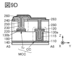
- FIGS. 9A to 9D show memory cell MCC in which part of the configuration of memory cell MCA is applied to memory cell MCB.
- the memory cell MCC has a transistor Tr and a capacitance element CC.
- the capacitance element CC has a conductive layer 115 whose upper surface is the same or approximately the same as the height of the upper surface of the insulating layer 180, a conductive layer 120, and an insulating layer 130a whose end is the same or approximately the same as the end of the conductive layer 120.
- an insulating layer 130b is provided below the conductive layer 220, and the end of the insulating layer 130b is the same or approximately the same as the end of the conductive layer 220.
- [Modification 3] 10A to 10D show a memory cell MCD.
- the memory cell MCD includes a transistor Tr and a capacitance element CD.
- the shapes of the conductive layer 120 and the insulating layer 130 of the capacitance element CD are different from the shapes of the conductive layer 120 and the insulating layer 130 of the capacitance element C.
- the conductive layer 115 has a protruding portion above the insulating layer 180. In other words, the top of the conductive layer 115 is located above the top surface of the insulating layer 180. In other words, the top surface of the insulating layer 180 is located below the top of the conductive layer 115 (on the insulating layer 140 side).
- the insulating layer 130 is provided so as to cover the protruding portion of the conductive layer 115.
- the insulating layer 130 has an area that contacts the upper surface of the conductive layer 115 in the opening 190, the upper and side surfaces of the protruding portion of the conductive layer 115, and the upper surface of the insulating layer 180 outside the opening 190.
- the conductive layer 120 is provided so as to fill the recess of the conductive layer 115 via the insulating layer 130. Furthermore, the conductive layer 120 has an area that faces a part of the outer side surface of the conductive layer 115 via the insulating layer 130. In other words, the end of the conductive layer 120 is located outside the conductive layer 115.
- FIGS. 11A to 11D show a memory cell MCE in which part of the configuration of the memory cell MCA is applied to the memory cell MCD.
- the memory cell MCE has a transistor Tr and a capacitance element CE.
- the capacitance element CE has a conductive layer 115 having the protruding portion, an insulating layer 130a provided to cover the protruding portion of the conductive layer 115, and a conductive layer 120 whose end coincides or roughly coincides with the end of the insulating layer 130a.
- the insulating layer 130b is provided below the conductive layer 220, and the end of the insulating layer 130b coincides or roughly coincides with the end of the conductive layer 220.
- the above-mentioned capacitance element can be said to have a cylindrical shape.
- the capacitance element of the memory cell is not limited to the configuration of the capacitance element described above, and capacitance elements having shapes such as parallel plate type or pillar type can be used.
- [Modification 4] 12A to 12D show a memory cell MCF.
- the memory cell MCF differs from the above-described memory cell MC mainly in that it has a conductive layer 261 and a conductive layer 265.
- An insulating layer 285 is provided on the insulating layer 250. As shown in FIG. 12B, the insulating layer 285 has an opening 293 and an opening 294 that overlaps with the opening 292. The height of the upper surface of the insulating layer 285 coincides with or approximately coincides with the height of the upper surface of the conductive layer 260.
- the conductive layer 261 is provided so as to fill the openings 294, 293, and 292.
- the conductive layer 261 contacts at least a portion of the upper surface of the conductive layer 120.
- the height of the upper surface of the conductive layer 261 coincides or approximately coincides with the height of the upper surface of the insulating layer 285.
- the conductive layer 265 is provided on the conductive layer 260 and on the insulating layer 285.
- the conductive layer 265 has a region in contact with the upper surface of the conductive layer 260 and a region in contact with the upper surface of the conductive layer 261.
- the conductive layer 260 is electrically connected to the conductive layer 120 via the conductive layer 265 and the conductive layer 261. That is, the memory cell MCF has a configuration in which the capacitance element C is connected to the gate of the transistor Tr. With this configuration, it is not necessary to extend the conductive layer 260 to a position where it overlaps with the capacitance element C. Therefore, the area where the conductive layer 260 and the conductive layer 240 overlap can be reduced. Furthermore, the insulating layer 281 and the insulating layer 250 are located between the conductive layer 265 and the conductive layer 240. This allows the physical distance between the conductive layer 265 and the conductive layer 240 to be increased, and the parasitic capacitance generated between the conductive layer 265 and the conductive layer 240 to be reduced.
- FIGS. 13A to 13D show a memory string 100B having a second gate.
- FIG. 13A is a plan view of the memory string 100B as viewed from the Z direction.
- FIG. 13B is an equivalent circuit of the memory string 100.
- FIG. 13C is a cross-sectional view of the portion A1-A2 shown by the dashed line in FIG. 13A as viewed from the Y direction.
- FIG. 13D is a cross-sectional view including the portion B1-B2 shown by the dashed line in FIG. 13A.
- Memory string 100B differs from memory string 100 above mainly in that it has conductive layers 215_1 to 215_n and insulating layers 225_1 to 225_n.
- Conductive layers 215_1 to 215_n are provided over the insulating layer 280.
- An insulating layer 281 is provided over the insulating layer 280 and the conductive layers 215_1 to 215_n.
- Conductive layers 240_1 to 240_k are provided over the insulating layer 281.
- the conductive layers 215_1 to 215_n correspond to the wirings BG_1 to BG_n, respectively.
- Memory string 100B has memory cells MCG_1 to MCG_n.
- the memory cell MCG has a transistor TrG and a capacitance element C.
- Transistor TrG has a conductive layer 260, an insulating layer 250, a conductive layer 215, an insulating layer 225, a conductive layer 220, a conductive layer 240, and a semiconductor layer 230.
- the conductive layer 215 extends in the Y direction. In other words, the conductive layer 215 extends in a direction parallel to the direction in which the conductive layer 110 extends.
- the conductive layer 215 has an opening that overlaps with the opening 290 and the opening 291.
- the insulating layer 281 has a first opening that overlaps with the opening 290 and the opening 291.
- the insulating layer 225 has an opening 291, a first opening in the insulating layer 281, an opening in the conductive layer 215, and a region disposed in the opening 290.
- the insulating layer 225 has a region in contact with the side of the conductive layer 240 in the opening 291, the side of the insulating layer 281 in the first opening, the side of the conductive layer 215 in the opening in the conductive layer 215, the side of the insulating layer 280 in the opening 290, and a part of the upper surface of the conductive layer 220 in the opening 290.
- the insulating layer 225 has an opening reaching the conductive layer 220 in a region overlapping the opening 290.
- the semiconductor layer 230 has an area that contacts the upper surface of the conductive layer 240, as well as the side surface of the insulating layer 225 in the opening of the insulating layer 225 and the upper surface of the conductive layer 220.
- the insulating layer 281 has a second opening that overlaps with the opening 292 and the opening 293.
- the conductive layer 260 has a region that is embedded in the opening 293, the second opening of the insulating layer 281, and the opening 292.
- the conductive layer 260 has a region that contacts the conductive layer 120 through the opening 293, the second opening, and the opening 292.
- the conductive layer 260 functions as a first gate electrode, and the insulating layer 250 functions as a first gate insulating layer.
- the conductive layer 215 functions as a second gate electrode, and the insulating layer 225 functions as a second gate insulating layer.
- the on and off states of the transistor can be controlled independently of the polarization held in the ferroelectric layer.
- the polarization of the ferroelectric layer can be maintained when switching the transistor between the on and off states.
- Example of manufacturing method As an example of a method for manufacturing a semiconductor device of one embodiment of the present invention, an example of a method for manufacturing the memory string 100 illustrated in FIG. 2A will be described below.
- A, C, and E in each figure are cross-sectional views of the semiconductor device viewed from the Y direction
- B, D, and F in each figure are cross-sectional views of the semiconductor device viewed from the X direction. Note that the cross-sectional views A, C, and E in each figure show an area including three memory cells, and the cross-sectional views B, D, and F in each figure show an area including one memory cell.
- the thin films (insulating films, semiconductor films, conductive films, etc.) that make up semiconductor devices can be formed using methods such as sputtering, ALD, chemical vapor deposition (CVD), vacuum deposition, molecular beam epitaxy (MBE), and pulsed laser deposition (PLD).
- ALD atomic layer deposition
- CVD chemical vapor deposition
- MBE molecular beam epitaxy
- PLD pulsed laser deposition
- CVD methods can also be classified into plasma CVD (PECVD) methods, which use plasma, thermal CVD (TCVD: Thermal CVD) methods, which use heat, and photo CVD (Photo CVD) methods, which use light. They can also be further classified into metal CVD (MCVD: Metal CVD) methods and metal organic CVD (MOCVD: Metal CVD) methods, depending on the source gas used.
- PECVD plasma CVD
- TCVD Thermal CVD
- Photo CVD Photo CVD
- MCVD Metal CVD
- MOCVD Metal CVD
- the plasma CVD method can produce high-quality films at relatively low temperatures.
- the thermal CVD method is a film formation method that can reduce plasma damage to the workpiece because it does not use plasma.
- wiring, electrodes, elements (transistors, capacitive elements, etc.) included in a semiconductor device may become charged up by receiving electric charge from the plasma. At this time, the accumulated electric charge may destroy the wiring, electrodes, elements, etc. included in the semiconductor device.
- thermal CVD method which does not use plasma, such plasma damage does not occur, so the yield of semiconductor devices can be increased.
- plasma damage does not occur during film formation, so a film with fewer defects can be obtained.
- the ALD method can be a thermal ALD method in which the reaction between the precursor and reactant is carried out using only thermal energy, or a PEALD method in which a plasma-excited reactant is used.
- the CVD and ALD methods are different from sputtering methods in which particles emitted from a target or the like are deposited. Therefore, they are film formation methods that are less affected by the shape of the workpiece and have good step coverage.
- the ALD method has excellent step coverage and excellent thickness uniformity, making it suitable for coating the surfaces of openings with high aspect ratios.
- the ALD method since the ALD method has a relatively slow film formation speed, it may be preferable to use it in combination with other film formation methods such as the CVD method, which has a fast film formation speed.
- a film of any composition can be formed by changing the flow rate ratio of the raw material gases.
- a film with a continuously changing composition can be formed by changing the flow rate ratio of the raw material gases while forming the film.
- a film of any composition can be formed by simultaneously introducing multiple different types of precursors.
- a film of any composition can be formed by controlling the number of cycles of each precursor.
- the thin films (insulating films, semiconductor films, conductive films, etc.) constituting the semiconductor device can be formed by wet film formation methods such as spin coating, dip coating, spray coating, inkjet printing, dispensing, screen printing, offset printing, doctor knife method, slit coating, roll coating, curtain coating, or knife coating.
- an insulating layer 140 is formed on a substrate (not shown), multiple conductive layers 110 are formed on the insulating layer 140, and an insulating layer 180 is formed on the insulating layer 140 and the multiple conductive layers 110. Note that in FIG. 14A, conductive layers 110_1 to 110_3 are shown as the multiple conductive layers 110.
- the insulating layer 180 functions as an interlayer insulating layer. It is preferable to use a material with a low dielectric constant for the insulating layer 180. This can reduce the parasitic capacitance that occurs between the conductive layer 110 and the conductive layer 220, and improve the operating speed of the semiconductor device.
- the insulating layer 180 may also have a laminated structure of multiple insulating layers, for example, a laminate of silicon oxide and silicon nitride.
- CMP chemical mechanical polishing
- the upper surface of the insulating layer 180 has an upwardly convex curved shape.
- each of the multiple openings 190 has an area that overlaps with one of the multiple conductive layers 110.
- Each of the multiple openings 190 reaches one of the multiple conductive layers 110.
- Figure 14D shows opening 190_1 reaching conductive layer 110_1.
- the opening 190 can be formed by forming a resist mask on the insulating layer 180 and performing an etching process using the resist mask as a mask. It is preferable to use an anisotropic dry etching process as the etching process, and to process the sidewall of the opening so that it is as vertical as possible. In this case, it is preferable that the shape of the opening is cylindrical.
- the resist mask can be formed by, for example, lithography, printing, inkjet, or the like.
- a photomask is not used, which may reduce the manufacturing cost.
- the dry etching method and the wet etching method can be used. Processing by the dry etching method is suitable for fine processing.
- a resist mask When forming a resist mask using lithography, first a resist is formed, and then the resist is exposed through a photomask. Next, the exposed or unexposed areas are removed using a developer to form a resist mask.
- a conductive layer, a semiconductor layer, an insulating layer, or the like can be processed into a desired shape.
- KrF excimer laser light, ArF excimer laser light, EUV (Extreme Ultraviolet) light, or the like can be used for exposure.
- Immersion technology may also be used.
- a beam such as an electron beam or an ion beam instead of the above-mentioned light, since this eliminates the need for a photomask.
- the resist mask can be removed by a wet etching process, a dry etching process, or both.
- a hard mask made of an inorganic material may be used instead of a resist mask.
- a film that will be the hard mask material is formed on the layer to be processed, a resist mask is formed on the film, and the film is etched to form a hard mask of the desired shape.
- a dry etching device for example, a capacitively coupled plasma (CCP) etching device having parallel plate electrodes or an inductively coupled plasma (ICP) etching device can be used.
- CCP capacitively coupled plasma
- ICP inductively coupled plasma
- a conductive film 115f which will later become the multiple conductive layers 115, is formed on the insulating layer 180.
- the conductive film 115f is preferably formed by a film formation method with high coverage such as an ALD method or a thermal CVD method. At this time, the conductive film 115f can be formed so that a part of it covers the opening 190.
- the conductive film 115f is processed by lithography to form multiple conductive layers 115.
- FIG. 15B shows conductive layer 115_1 of the multiple conductive layers 115.
- the conductive film 115f can be processed by dry etching or wet etching. Dry etching is suitable for fine processing. By this processing, the conductive layer 115 is formed so as to contact the sidewall and bottom surface of the opening 190. The conductive layer 115 has a recess in the area that overlaps with the opening 190. Note that when processing the conductive film 115f, a part of the insulating layer 180 is processed, and the thickness of the insulating layer 180 in the area that does not overlap with the conductive layer 115 may become thin.
- the conductive film 115f may be processed by a method other than the above-mentioned lithography method. For example, a sacrificial layer may be formed to fill the opening 190, a planarization process may be performed to expose the upper surface of the insulating layer 180, and a process of removing the sacrificial layer may be performed. By this process, the conductive layer 115 shown in FIG. 8C and FIG. 8D can be formed.
- an insulating layer 130 and a conductive film 120f are formed in this order on the insulating layer 180 and the multiple conductive layers 115.
- the insulating layer 130 is preferably formed using a film formation method with high coverage so that the insulating layer 130 is formed along the recesses of the conductive layer 115. Furthermore, the conductive film 120f is preferably formed so as to fill the recesses.
- the insulating layer 130 can be formed by the ALD method, and the conductive film 120f can be formed by the CVD method.
- hafnium zirconium oxide is formed as the insulating layer 130 by the ALD method
- a precursor containing hafnium, a precursor containing zirconium, and an oxidizing agent can be used.
- the precursor containing hafnium tetrakis(ethylmethylamido)hafnium (TEMAHf), HfCl4 , etc.
- the precursor containing zirconium tetrakis(ethylmethylamido)zirconium (TEMAZr), ZrCl4 , etc.
- the oxidizing agent any one or more selected from O2 , O3 , N2O , NO2 , H2O , and H2O2 can be used.
- an oxide containing, in addition to hafnium and zirconium, a Group 3 element such as scandium, yttrium, or lanthanum for the insulating layer 130.
- an inorganic compound or an organic compound containing the target element can be used as a precursor containing a Group 3 element such as scandium, yttrium, or lanthanum.
- the precursor may be liquid or solid at room temperature and pressure.
- yttrium compounds such as tris(methylcyclopentadienyl)yttrium(III) (Y(MeCp) 3 ), tris(isopropylcyclopentadienyl)yttrium(III) (Y(iPrCp) 3 ), and tris[N,N-bis(trimethylsilyl)amide]yttrium(III) (Y(tmsa) 3 ) can be mentioned.
- examples of precursors containing lanthanum include lanthanum compounds such as tris(cyclopentadienyl)lanthanum(III) (La(Cp) 3 ), tris(methylcyclopentadienyl)lanthanum(III) (La(MeCp) 3 ), and tris(isopropylcyclopentadienyl)lanthanum(III) (La(iPrCp) 3 ).
- lanthanum compounds such as tris(cyclopentadienyl)lanthanum(III) (La(Cp) 3 ), tris(methylcyclopentadienyl)lanthanum(III) (La(MeCp) 3 ), and tris(isopropylcyclopentadienyl)lanthanum(III) (La(iPrCp) 3 ).
- the heat treatment crystallizes the insulating layer 130, so that the insulating layer 130 exhibits ferroelectricity.
- the heat treatment can increase the ferroelectricity of the insulating layer 130.
- the higher the temperature of the heat treatment the more the crystallization is promoted and the greater the remanent polarization, which is preferable.
- the heat treatment is preferably performed before forming a semiconductor film (semiconductor film 230f described later) that will later become multiple semiconductor layers, and more preferably before forming the insulating layer 280 described later.
- the semiconductor layer 230 is formed after the heat treatment, which prevents the oxide semiconductor from becoming polycrystallized, and thus realizes a highly reliable transistor.
- the heat treatment for crystallizing the insulating layer 130 is preferably performed in a state where the insulating layer 130 is in contact with the conductive layer 115, or in a state where the insulating layer 130 is in contact with the conductive layer 115 and the conductive layer 120 (or the conductive film 120f).
- an RTA (Rapid Thermal Anneal) device for example, an RTA (Rapid Thermal Anneal) device, a resistance heating furnace, or a microwave heating device can be used for the heat treatment.
- the use of an RTA device is preferable because it is possible to apply a high temperature in a short time, thereby enhancing the ferroelectricity of the insulating layer 130, shortening the process time, and reducing thermal damage to layers other than the insulating layer 130.
- the heat treatment is preferably performed in an inert gas or reducing gas atmosphere, since it is possible to suppress oxidation of the electrodes.
- the inert gas for example, noble gases such as helium, argon, and neon, and nitrogen gas can be used.
- the reducing gas for example, hydrogen gas, carbon monoxide gas, and hydrocarbon gas can be used.
- the crystal structure exhibiting ferroelectricity is not a stable structure (stable phase) but is classified as a metastable phase that appears at relatively high temperatures. Therefore, by heating at high temperatures using the RTA method and then rapidly cooling, the metastable phase in the film is maintained, and an insulating layer 130 containing many crystal structures exhibiting ferroelectricity can be formed.
- an LRTA (Lamp Rapid Thermal Anneal) device As the RTA device, an LRTA (Lamp Rapid Thermal Anneal) device, a GRTA (Gas Rapid Thermal Anneal) device, etc. can be used.
- the LRTA device is a device that heats the workpiece by radiating light (electromagnetic waves) emitted from a lamp such as a halogen lamp, a metal halide lamp, a xenon arc lamp, a carbon arc lamp, a high-pressure sodium lamp, or a high-pressure mercury lamp.
- the GRTA device is a device that performs heat treatment using a high-temperature gas.
- the gas used is a noble gas such as helium, neon, or argon, or an inert gas such as nitrogen that does not react with the workpiece during heat treatment.
- the treatment temperature can be 300°C to 750°C, preferably 400°C to 700°C, more preferably 500°C to 650°C.
- the treatment time can be 1 second to 10 minutes, preferably 3 seconds to 5 minutes, more preferably 5 seconds to 1 minute.
- an RTA device using a halogen lamp (LRTA device) can be used for the heat treatment, and the treatment can be performed for 1 minute at a treatment temperature of 600°C in a nitrogen atmosphere.
- the treatment time excluding the temperature rise period and the temperature fall period can be 1 minute to 5 hours, preferably 1 minute to 2 hours.
- the conductive film 120f is processed by lithography to form a plurality of conductive layers 120 and a plurality of conductive layers 220.
- FIG. 15E shows conductive layer 220_1 and conductive layer 220_2 out of the plurality of conductive layers 220.
- FIG. 15F shows conductive layer 120_1 out of the plurality of conductive layers 120 and conductive layer 220_1 out of the plurality of conductive layers 220.
- the processing method of the conductive film 120f refer to the description of the processing of the conductive film 115f described above.
- One conductive layer 220 is formed so as to overlap two conductive layers 110 adjacent in the A1-A2 direction.
- conductive layer 220_1 is formed so as to have an area overlapping with conductive layer 110_1 and an area overlapping with conductive layer 110_2.
- conductive layer 120 and conductive layer 220 are formed in the same process. Therefore, conductive layer 220 has the same conductive material as conductive layer 120.
- the capacitive element C is formed.
- the insulating layer 130 may be processed after processing the conductive film 120f.
- the conductive film 120f and the insulating layer 130 may be processed at the same time, or the processing conditions may be changed for the conductive film 120f and the insulating layer 130.
- the thickness of the insulating layer 180 in the region that does not overlap with the conductive layer 120 and the insulating layer 130a, and the region that does not overlap with the conductive layer 220 and the insulating layer 130b may become thin.
- Insulating layer 130a and insulating layer 130b are formed in the same process. Therefore, insulating layer 130b has the same insulating material as insulating layer 130a.
- an insulating layer 280 is formed on the insulating layer 130, the plurality of conductive layers 120, and the plurality of conductive layers 220. Since the insulating layer 280 functions as an interlayer insulating layer, an insulating material applicable to the insulating layer 180 can be used.
- the conductive film 240f can be suitably formed.
- the upper surface of the insulating layer 280 has an upwardly convex curved shape. By not performing the planarization process, it is possible to reduce manufacturing costs and increase production yields.
- a conductive film 240f which will later become the multiple conductive layers 240, is formed on the insulating layer 280.
- a plurality of openings are formed in the conductive film 240f and the insulating layer 280.
- Each of the plurality of openings has an area overlapping one of the plurality of conductive layers 220.
- Each of the plurality of openings reaches one of the plurality of conductive layers 220.
- Each of the plurality of openings includes an opening 291 and an opening 290.
- FIG. 16C shows openings 291_1, 291_2, and 291_3 formed in the conductive film 240f, and openings 290_1, 290_2, and 290_3 formed in the insulating layer 280.
- FIG. 16D shows opening 291_1 formed in the conductive film 240f, and opening 290_1 formed in the insulating layer 280.
- openings 291 and 290 For the method of forming openings 291 and 290, please refer to the explanation of the formation of openings 190 described above.
- a semiconductor film 230f which will later become the multiple semiconductor layers 230, is formed on the conductive film 240f.
- the semiconductor film 230f is preferably formed by a film formation method with high coverage such as the ALD method.
- the semiconductor film 230f can be formed so that a part of it covers the openings 291 and 290.
- an oxide film containing indium can be formed by the ALD method as the semiconductor film 230f.
- the deposition of the semiconductor film 230f is not limited to the above, and may be performed using a sputtering method, a CVD method, a PLD method, an MBE method, or the like.
- the crystallinity of the semiconductor material used for the semiconductor layer 230 is not particularly limited, and any of an amorphous semiconductor (a semiconductor having an amorphous structure), a single crystal semiconductor (a semiconductor having a single crystal structure), and a semiconductor having crystallinity other than single crystal (a microcrystalline semiconductor, a polycrystalline semiconductor, or a semiconductor having a crystalline region in part) may be used.
- a single crystal semiconductor or a semiconductor having crystallinity is preferable because it can suppress deterioration of the transistor characteristics.
- the semiconductor layer 230 preferably has a metal oxide layer having crystallinity.
- the structure of the metal oxide having crystallinity include a CAAC structure, a polycrystalline structure, and a microcrystalline structure.
- the CAAC structure is a crystal structure in which multiple microcrystals (typically multiple IGZO microcrystals) have a c-axis orientation, and the multiple microcrystals are connected without being oriented in the a-b plane.
- the OS film having a CAAC structure can also be said to have a structure having layered crystal parts.
- the polycrystalline structure has grain boundaries.
- a minute gap also called a nanocrack or microcrack
- a minute space also called a nanospace or microspace
- the electrical resistance of the oxide semiconductor layer increases. This is because the electrical resistance of the minute gap or minute space is very high, for example, infinite.
- an oxide semiconductor layer having a minute gap or minute space is used in a channel formation region of a transistor, the contact resistance between the oxide semiconductor layer and one or both of the source electrode and the drain electrode increases. This adversely affects the initial characteristics or reliability of the transistor. Since the CAAC structure does not have a clear grain boundary (grain boundary) on the a-b plane, a semiconductor device with higher reliability than that of the polycrystalline structure can be realized.
- the semiconductor layer 230 can have a stacked structure of two or more metal oxide layers with different crystallinity.
- the two or more metal oxide layers may have different compositions, or may have the same or approximately the same composition.
- the surface on which the second metal oxide layer is formed becomes the surface of the first metal oxide layer, so that the crystallinity of the second metal oxide layer can be increased in some cases.
- a heat treatment also called a crystallization treatment
- the crystallinity of the first metal oxide layer can be increased.
- a first metal oxide layer is formed using the ALD method, and a second metal oxide layer is formed using a sputtering method to have a higher crystallinity than the first metal oxide layer. Then, a heat treatment is performed to improve the crystallinity of the first and second metal oxide layers. At this time, the crystals contained in the second metal oxide layer grow continuously in the vertical direction toward the first metal oxide layer, and the boundary between the first and second metal oxide layers may become difficult to recognize by cross-sectional observation.
- a three-layer structure may be formed by forming a third metal oxide layer on the second metal oxide layer using the ALD method. After forming the third metal oxide layer, a heat treatment can be performed to improve the crystallinity of the first to third metal oxide layers. In this case, the crystals contained in the second metal oxide layer grow continuously in the vertical direction toward the first metal oxide layer and the third metal oxide layer, and then grow laterally as well, so that the boundary between the first metal oxide layer and the second metal oxide layer, and the boundary between the second metal oxide layer and the third metal oxide layer, may not be recognized by cross-sectional observation.
- ALD method For example, if a three-layer structure is formed by depositing a first metal oxide layer using the ALD method, depositing a film having a CAAC structure as a second metal oxide layer using the sputtering method, and depositing a third metal oxide layer using the ALD method, the crystallinity of the upper and lower metal oxide layers can be enhanced using the CAAC structure of the second metal oxide layer as a nucleus or seed.
- a metal oxide layer with enhanced crystallinity in this way can be called Axial Growth CAAC (AG CAAC).
- the above heat treatment is preferably performed at a temperature lower than that of the heat treatment for crystallizing the insulating layer 130.
- the heat treatment is preferably carried out at a temperature of 250°C or higher and 650°C or lower, and more preferably at a temperature of 350°C or higher and 550°C or lower.
- the treatment time is preferably, for example, 1 minute or higher and 1 hour or lower, or 10 minutes or higher and 30 minutes or lower, at a temperature of 350°C or higher and 550°C or lower.
- the heating device used for the heat treatment is not particularly limited, and may be a device that heats the workpiece by thermal conduction or thermal radiation from a heating element such as a resistive heating element.
- a heating element such as a resistive heating element.
- an electric furnace or an RTA device such as an LRTA device or a GRTA device may be used.
- FIG. 17A and FIG. 17B the semiconductor film 230f and the conductive film 240f are processed by lithography to form a plurality of semiconductor layers 230 and a plurality of conductive layers 240, respectively.
- FIG. 17A shows the semiconductor layer 230_1 and the semiconductor layer 230_2 of the plurality of semiconductor layers 230, and the conductive layer 240_1 and the conductive layer 240_2 of the plurality of conductive layers 240.
- FIG. 17B shows the semiconductor layer 230_1 of the plurality of semiconductor layers 230 and the conductive layer 240_1 of the plurality of conductive layers 240.
- the semiconductor film 230f and the conductive film 240f can be processed using a dry etching method or a wet etching method. Processing using a dry etching method is suitable for fine processing. By this processing, the semiconductor layer 230 is formed so as to contact the sidewall of the opening 291 and the sidewall and bottom surface of the opening 290. Furthermore, the semiconductor layer 230 has a recess in the area overlapping the opening 291 and the opening 290. Furthermore, the semiconductor film 230f and the conductive film 240f may be processed under the same conditions or different conditions.
- One conductive layer 240 is formed so as to overlap two conductive layers 220 adjacent in the A1-A2 direction.
- conductive layer 240_2 is formed so as to have an area overlapping with conductive layer 220_1 and an area overlapping with conductive layer 220_2.
- the multiple conductive layers 220 and the multiple conductive layers 240 as described above, a configuration can be achieved in which the first transistor and the second transistor adjacent in the A1-A2 direction share one of the conductive layers 220 and 240, and the second transistor and the third transistor adjacent in the A1-A2 direction share the other of the conductive layers 220 and 240. This allows the memory string 100 to have a configuration in which multiple transistors are connected in series.
- the insulating layer 250 is formed on the insulating layer 280 and the multiple semiconductor layers 230.
- the insulating layer 250 is preferably formed by a film forming method with high coverage. At this time, the insulating layer 250 can be formed so that a part of it covers the recessed portion described above.
- the insulating layer 250 is preferably formed by, for example, a CVD method or an ALD method. In particular, it is preferable to use the ALD method to stack multiple different insulating films.
- an insulating film having a barrier property against oxygen for the insulating layer 250.
- an insulating film having a function of capturing or fixing hydrogen for the insulating layer 250.
- a laminated film of aluminum oxide and hafnium oxide can be used for the insulating layer 250. Since aluminum oxide and hafnium oxide are high dielectric constant (high-k) materials, using these for the gate insulating layer makes it possible to reduce the gate potential applied during transistor operation while maintaining the physical thickness of the gate insulating layer. In other words, it becomes possible to reduce the equivalent oxide thickness (EOT) of the gate insulating layer.
- high-k high dielectric constant
- a silicon oxide film or a silicon oxynitride film with high dielectric strength for the insulating layer 250. This can reduce the leakage current of the transistor.
- an insulating film having a barrier property against hydrogen may be provided on the side of the insulating layer 250 that contacts the conductive layer 260. This can suppress the diffusion of impurities such as hydrogen contained in the conductive layer 260 into the semiconductor layer 230.
- insulating films having a barrier property against hydrogen include silicon nitride films, silicon nitride oxide films, aluminum oxide films, and aluminum nitride films. In particular, silicon nitride films are preferable because they have high barrier properties against hydrogen.
- such insulating films have barrier properties against oxygen in addition to hydrogen, and can block oxygen diffusing from the semiconductor layer 230 to the conductive layer 260, thereby preventing the conductive layer 260 from being oxidized.
- the thickness of each film is preferably 0.5 nm to 15 nm, more preferably 0.5 nm to 12 nm, and even more preferably 0.5 nm to 10 nm.
- a laminated film of an aluminum oxide film with a thickness of 1 nm, a silicon oxide film with a thickness of 2 nm, and a hafnium oxide film with a thickness of 2 nm can be used from the semiconductor layer 230 side.
- a laminated film in which a silicon nitride film with a thickness of 1 nm is laminated on the conductive layer 260 side may be used.
- the film thickness is not limited to the above, and for example, the thickness of any one or more of the films may be 15 nm or more.
- a plurality of openings are formed in the insulating layer 250 and the insulating layer 280.
- Each of the plurality of openings has an area that overlaps with one of the plurality of conductive layers 120.
- Each of the plurality of openings reaches one of the plurality of conductive layers 120.
- Each of the plurality of openings includes an opening 293 and an opening 292. Note that FIG. 17D shows an opening 292_1 that reaches the conductive layer 120_1, and an opening 293_1 that overlaps with the opening 292_1.
- openings 293 and 292 For the method of forming openings 293 and 292, refer to the explanation of the formation of opening 190 described above.
- the conductive film is preferably formed so as to fill the openings 291 and 290, as well as the openings 293 and 292.
- the conductive film can be formed by a CVD method.
- FIG. 17E and FIG. 17F the conductive film is processed by lithography to form a plurality of conductive layers 260.
- FIG. 17E shows conductive layer 260_1, conductive layer 260_2, and conductive layer 260_3 out of the plurality of conductive layers 260.
- FIG. 17F shows conductive layer 260_1 out of the plurality of conductive layers 260.
- the conductive layer can be processed by dry etching or wet etching. Dry etching is suitable for fine processing. By this processing, the conductive layer 260 is formed so as to fill the openings 293 and 292, and the openings 292 and 291.
- an insulating layer 283 is formed on the insulating layer 250 and the multiple conductive layers 260 to create a memory string ( Figures 2C and 2E).
- Figure 18 is a block diagram showing an example of the configuration of the circuit OSC and the memory cell unit MCL.
- the memory cell unit MCL is a circuit that includes the memory cells and memory strings described above.
- the memory cell unit MCL has a memory cell array MCAA.
- the memory cell array MCAA has multiple memory strings SRG.
- the memory strings SRG are electrically connected to wiring BL.
- the memory strings SRG have multiple memory cells MC electrically connected in series, and selection transistors BTr and STr.
- the memory cell MC is a transistor that operates with normally-on characteristics, and has a control gate and a functional layer.
- a ferroelectric layer can be used as the functional layer.
- a configuration using a ferroelectric layer as the functional layer can be a configuration in which a ferroelectric capacitor is connected to the gate as exemplified above.
- the functional layer corresponds to the insulating layer 130 described above.
- the channel formation regions of the transistor BTr, memory cell MC, and transistor STr preferably have one or more materials selected from the following: silicon, germanium, gallium arsenide, silicon carbide, metal oxide, etc.
- the metal oxide can be used as a wide-gap semiconductor, and can impart characteristics of extremely small off-current to the transistor BTr, memory cell MC, and transistor STr in which the metal oxide is included in the channel formation region. In other words, since the leakage current in the transistor BTr, memory cell MC, and transistor STr in the off state can be reduced, the power consumption of the storage device can be reduced in some cases.
- FIG. 18 shows an example in which the transistors BTr and STr are formed in the memory cell unit MCL, the transistors BTr and STr may also be formed in the circuit OSC.
- the memory cell array MCAA has multiple memory cells MC in the memory string SRG.
- the multiple memory cells MC are arranged in a matrix.
- the memory cell array MCAA has n memory cells MC in each column and m memory cells MC in each row, for a total of n x m memory cells MC (m and n are each independently an integer of 2 or more).
- the memory cell MC located in row i and column j (i is an integer of 1 or more and n or less, and j is an integer of 1 or more and m or less) is represented as MC[i, j].
- the wiring WL is a plurality of word lines, each of which is electrically connected to a memory cell MC for each row.
- the wiring BL is a plurality of bit lines, each of which is electrically connected to a memory cell MC for each column.
- the wiring CL is a power supply line.
- the transistor BTr, the memory cells MC, and the transistor STr are connected in series, and the transistor BTr is electrically connected to the wiring BSL, and the transistor STr is electrically connected to the wiring SSL.
- the wiring BSL and the wiring SSL function as wirings for selecting a memory string when performing operations such as writing, reading, and erasing.
- the wiring BSL is electrically connected to the gate of the transistor BTr
- the wiring SSL is electrically connected to the gate of the transistor STr.
- the memory cell portion MCL may have a configuration in which multiple memory strings SRG are electrically connected to one wiring BL.
- the block diagram in FIG. 19 illustrates the memory cell portion MCL and a part of the circuit OSC.
- the circuit OSC has a control circuit CTR, a circuit PRPH, and an output circuit OUTP.
- the control circuit CTR receives, for example, control signals CS (clock signal, chip enable signal, write enable signal, address signal, etc.) and a data signal WDATA from outside the memory device.
- the control circuit CTR has a function of accessing the circuit PRPH to write data to the memory cell unit MCL and a function of reading data from the memory cell unit MCL. For example, when a write command based on a control signal CS and a data signal WDATA are input from outside the memory device, the control circuit CTR writes the data signal WDATA to the memory cell unit MCL. In addition, in response to a read command based on the control signal CS, the control circuit CTR reads data from the memory cell unit MCL and outputs it as a data signal RDATA. Note that the write command and read command include an address signal.
- the control circuit CTR may also have a function of detecting and correcting errors (also called ECC: Error Check and Correct) when reading data from the memory cell unit MCL.
- ECC Error Check and Correct
- the circuit PRPH includes, for example, a circuit WLD, a circuit BLD, and a circuit CVC.
- the circuit WLD functions as a word line driver circuit and is electrically connected to the wiring WL.
- the circuit BLD functions as a bit line driver circuit and is electrically connected to the wiring BL.
- the circuit CVC functions as a power supply that generates a constant potential and outputs the constant potential and is electrically connected to the wiring CL.
- the circuit CVC may not be included in the circuit PRPH and may be provided outside the memory device. In this case, the memory device is configured such that a constant potential is applied to the memory cell unit MCL from outside.
- Figure 20A shows a block diagram of the arithmetic processing device 1100.
- Figure 20A shows an example of a CPU configuration as an example of a configuration that can be used for the arithmetic processing device 1100.
- the arithmetic processing device 1100 shown in FIG. 20A has an ALU 1191 (ALU: Arithmetic logic unit, arithmetic circuit), an ALU controller 1192, an instruction decoder 1193, an interrupt controller 1194, a timing controller 1195, a register 1196, a register controller 1197, a bus interface 1198), a cache 1199, and a cache interface 1189 on a substrate 1190.
- the substrate 1190 is a semiconductor substrate, an SOI (Silicon On Insulator) substrate, a glass substrate, or the like. It may have a rewritable ROM and a ROM interface.
- the cache 1199 and the cache interface 1189 may be provided on separate chips.
- the cache 1199 is connected to a main memory provided on a separate chip via a cache interface 1189.
- the cache interface 1189 has a function of supplying a portion of the data stored in the main memory to the cache 1199.
- the cache 1199 has a function of storing that data.
- the arithmetic processing device 1100 shown in FIG. 20A is merely one example of a simplified configuration, and the actual arithmetic processing device 1100 has a wide variety of configurations depending on the application.
- the arithmetic processing device 1100 shown in FIG. 20 or a configuration including an arithmetic circuit may be one core, and a configuration including multiple such cores may be configured so that each core operates in parallel, that is, a configuration like a GPU.
- the number of bits that the arithmetic processing device 1100 can handle in the internal arithmetic circuit or data bus may be, for example, 8 bits, 16 bits, 32 bits, 64 bits, etc.
- Instructions input to the arithmetic processing unit 1100 via the bus interface 1198 are input to the instruction decoder 1193, decoded, and then input to the ALU controller 1192, the interrupt controller 1194, the register controller 1197, and the timing controller 1195.
- the ALU controller 1192, interrupt controller 1194, register controller 1197, and timing controller 1195 perform various controls based on the decoded instructions. Specifically, the ALU controller 1192 generates a signal for controlling the operation of the ALU 1191. Furthermore, while the arithmetic processing device 1100 is executing a program, the interrupt controller 1194 determines and processes interrupt requests from external input/output devices or peripheral circuits based on their priority or mask state. The register controller 1197 generates an address for the register 1196, and reads or writes to the register 1196 depending on the state of the arithmetic processing device 1100.
- the timing controller 1195 also generates signals that control the timing of the operations of the ALU 1191, the ALU controller 1192, the instruction decoder 1193, the interrupt controller 1194, and the register controller 1197.
- the timing controller 1195 includes an internal clock generating unit that generates an internal clock signal based on a reference clock signal, and supplies the internal clock signal to the various circuits described above.
- a memory device is provided in the register 1196 and the cache 1199.
- the register controller 1197 selects the holding operation in the register 1196 according to instructions from the ALU 1191. That is, it selects whether the memory cells in the register 1196 will hold data using flip-flops or using capacitive elements. If holding data using flip-flops is selected, a power supply voltage is supplied to the memory cells in the register 1196. If holding data in capacitive elements is selected, the data is rewritten to the capacitive elements, and the supply of power supply voltage to the memory cells in the register 1196 can be stopped.
- the arithmetic processing device 1100 is not limited to a CPU, but may be a GPU, a DSP (Digital Signal Processor), an FPGA (Field-Programmable Gate Array), etc.
- the semiconductor device 1000 having the memory device exemplified above and the arithmetic processing device 1100 can be provided overlapping each other.
- Figs. 20B and 20C show perspective views of the semiconductor device 1150A.
- the semiconductor device 1150A has the semiconductor device 1000 functioning as a memory device on the arithmetic processing device 1100.
- the arithmetic processing device 1100 and the semiconductor device 1000 have overlapping regions. To make the configuration of the semiconductor device 1150A easier to understand, the arithmetic processing device 1100 and the semiconductor device 1000 are shown separately in Fig. 20C.
- connection distance between them can be shortened. This allows the communication speed between them to be increased. In addition, the short connection distance allows power consumption to be reduced.
- FIGS. 21A and 21B show perspective views of the semiconductor device 1150B.
- the semiconductor device 1150B has a semiconductor device 1000a and a semiconductor device 1000b on the arithmetic processing device 1100.
- the arithmetic processing device 1100, the semiconductor device 1000a, and the semiconductor device 1000b have overlapping regions.
- FIG. 21B shows the arithmetic processing device 1100, the semiconductor device 1000a, and the semiconductor device 1000b separately.
- the semiconductor device 1000a and the semiconductor device 1000b function as memory devices.
- one of the semiconductor device 1000a and the semiconductor device 1000b may be used as a NOR type memory device, and the other may be used as a NAND type memory device.
- Both the semiconductor device 1000a and the semiconductor device 1000b may be NAND type memory devices.
- Examples of NOR type memory devices include DRAM and SRAM. Since NOR type memory devices can operate faster than NAND type memory devices, for example, a part of the semiconductor device 1000a can be used as a main memory and/or cache 1199. Note that the stacking order of the semiconductor device 1000a and the semiconductor device 1000b may be reversed.
- Figures 21C and 21D show perspective views of semiconductor device 1150C.
- Semiconductor device 1150C has a configuration in which arithmetic processing device 1100 is sandwiched between semiconductor device 1000a and semiconductor device 1000b.
- the semiconductor device 1150C By configuring the semiconductor device 1150C, it is possible to increase the communication speed between the semiconductor device 1000a and the arithmetic processing device 1100, and the communication speed between the semiconductor device 1000b and the arithmetic processing device 1100. In addition, it is possible to reduce power consumption compared to the semiconductor device 1150B.
- Figure 22A shows an example of a case where a layer 11 including a transistor 300 and a layer 12 including multiple memory strings are stacked.
- a circuit using a single crystal silicon substrate as the substrate can be applied as layer 11, and a memory device having a three-dimensional NAND type memory can be applied as layer 12.
- layer 11 is the arithmetic processing device 1100 exemplified above
- layer 12 is the semiconductor device 1000 that functions as a memory device.
- FIG. 22A illustrates one memory string.
- FIG. 22B illustrates a cross-sectional view of a region including transistor 142 as viewed from the X direction. Note that layer 11 is omitted in FIG. 22B.
- Each memory string provided in layer 12 has transistor 142, transistor 141 that each of the multiple memory cells has, and transistor 143. Note that detailed explanations of the configuration of layer 12 that can be referred to memory string 100 illustrated in FIG. 2A and other figures will be omitted, and only the differences will be explained.
- the transistor 300 included in the layer 11 is provided over a substrate 311, and includes a conductive layer 316, an insulating layer 315, a semiconductor region 313 formed of a part of the substrate 311, and a low-resistance region 314a and a low-resistance region 314b functioning as a source region or a drain region.
- FIG. 22A shows a cross section of the transistor 300 in the channel length direction.
- the transistor 300 is preferably a so-called Fin-type transistor in which the upper surface and the side surface in the channel width direction of the semiconductor region 313 are covered with the conductive layer 316 via the insulating layer 315 in the cross section in the channel width direction. This increases the effective channel width, improving the on-characteristics of the transistor 300. In addition, the contribution of the electric field of the gate electrode can be increased, improving the off-characteristics of the transistor 300.
- the transistor 300 may be either a p-channel type or an n-channel type.
- the region where the channel of the semiconductor region 313 is formed, the region nearby, the low resistance region 314a and the low resistance region 314b which become the source region or drain region, etc. preferably contain a semiconductor such as a silicon-based semiconductor, and preferably contain single crystal silicon.
- they may be formed of a material containing Ge (germanium), SiGe (silicon germanium), GaAs (gallium arsenide), GaN (gallium nitride), GaAlAs (gallium aluminum arsenide), etc.
- a configuration using silicon in which the effective mass is controlled by applying stress to the crystal lattice and changing the lattice spacing may be used.
- the transistor 300 may be a HEMT (High Electron Mobility Transistor) by using GaAs and GaAlAs, etc.
- Low resistance region 314a and low resistance region 314b contain, in addition to the semiconductor material applied to semiconductor region 313, an element that imparts n-type conductivity, such as arsenic or phosphorus, or an element that imparts p-type conductivity, such as boron.
- the conductive layer 316 that functions as the gate electrode can be made of a conductive material such as a semiconductor material, metal material, alloy material, or metal oxide material, such as silicon containing an element that imparts n-type conductivity, such as arsenic or phosphorus, or an element that imparts p-type conductivity, such as boron.
- a conductive material such as a semiconductor material, metal material, alloy material, or metal oxide material, such as silicon containing an element that imparts n-type conductivity, such as arsenic or phosphorus, or an element that imparts p-type conductivity, such as boron.
- the work function is determined by the material of the conductor, so the threshold voltage (Vth) of the transistor can be adjusted by changing the material of the conductor.
- Vth threshold voltage
- materials such as titanium nitride and tantalum nitride for the conductor.
- metal materials such as tungsten and aluminum as a laminate for the conductor, and in particular, using tungsten is preferable in terms of heat resistance.
- transistor 300 shown in FIG. 22A is just one example, and the present invention is not limited to this structure. An appropriate transistor may be used depending on the circuit configuration, driving method, etc.
- An insulating layer 320, an insulating layer 322, an insulating layer 324, and an insulating layer 326 are stacked in this order to cover the transistor 300.
- insulating layer 320 As insulating layer 320, insulating layer 322, insulating layer 324, and insulating layer 326, for example, silicon oxide, silicon oxynitride, silicon nitride oxide, silicon nitride, aluminum oxide, aluminum oxynitride, aluminum nitride oxide, aluminum nitride, etc. may be used.
- the insulating layer 322 may function as a planarizing film that flattens steps caused by the transistor 300 or the like provided below it.
- the top surface of the insulating layer 322 may be planarized by a planarization process using a CMP process or the like to improve flatness.
- a film for the insulating layer 324 that has barrier properties to prevent hydrogen, impurities, and the like from diffusing from the substrate 311 or the transistor 300 to the region in which the transistor 141 and the like are provided.
- a film having a barrier property against hydrogen for example, silicon nitride formed by a CVD method can be used.
- silicon nitride formed by a CVD method when hydrogen diffuses into a semiconductor element having an oxide semiconductor such as the transistor 141, the characteristics of the semiconductor element may deteriorate. Therefore, it is preferable to use a film that suppresses hydrogen diffusion between the transistor 141 and the transistor 300.
- the film that suppresses hydrogen diffusion is a film that releases a small amount of hydrogen.
- the amount of desorption of hydrogen can be analyzed, for example, by using thermal desorption spectrometry (TDS).
- TDS thermal desorption spectrometry
- the amount of desorption of hydrogen from the insulating layer 324 is preferably 10 ⁇ 10 15 atoms/cm 2 or less, and more preferably 5 ⁇ 10 15 atoms/cm 2 or less , converted into hydrogen atoms per area of the insulating layer 324, when the film surface temperature is in the range of 50° C. to 500° C.
- the insulating layer 326 has a lower dielectric constant than the insulating layer 324.
- the dielectric constant of the insulating layer 326 is preferably less than 4, and more preferably less than 3.
- the dielectric constant of the insulating layer 326 is preferably 0.7 times or less, and more preferably 0.6 times or less, the dielectric constant of the insulating layer 324.
- conductive layers 328 and 330 are embedded in insulating layers 320, 322, 324, and 326. Conductive layers 328 and 330 function as plugs or wiring.
- a conductor that functions as a plug or wiring may have multiple structures collectively given the same symbol.
- the wiring and the plug that connects to the wiring may be integrated. That is, there are cases where a part of the conductor functions as the wiring, and cases where a part of the conductor functions as the plug.
- a conductive material such as a metal material, an alloy material, a metal nitride material, or a metal oxide material can be used in a single layer or a stacked layer. It is preferable to use a high melting point material such as tungsten or molybdenum that has both heat resistance and conductivity, and it is preferable to use tungsten. Alternatively, it is preferable to form it from a low resistance conductive material such as aluminum or copper. By using a low resistance conductive material, the wiring resistance can be reduced.
- a wiring layer may be provided on the insulating layer 326 and the conductive layer 330.
- a conductor having a barrier property against hydrogen for example, tantalum nitride or the like can be used.
- tantalum nitride and tungsten which has high conductivity, it is possible to suppress diffusion of hydrogen from the transistor 300 while maintaining the conductivity as a wiring.
- the tantalum nitride layer having a barrier property against hydrogen is in contact with an insulator having a barrier property against hydrogen. Note that in FIG. 22A, an insulating layer 350 having a barrier property against hydrogen is provided on the insulating layer 326 and the conductive layer 330.
- Layer 12 includes an insulating layer 140, multiple conductive layers 110, an insulating layer 180, an insulating layer 130, multiple conductive layers 220, an insulating layer 280, multiple conductive layers 240, multiple semiconductor layers 230, an insulating layer 250, multiple conductive layers 260, a conductive layer 262, a conductive layer 263, an insulating layer 283, an insulating layer 284, etc.
- Transistor 142 and transistor 143 function as selection transistors.
- Conductive layer 262 has a region that functions as the gate electrode of transistor 142, and conductive layer 263 has a region that functions as the gate electrode of transistor 143.
- Conductive layer 262 extends in the Y direction, and a capacitance element consisting of conductive layer 115, insulating layer 130, and conductive layer 120 is not provided in the insulating layer 180 in the region that overlaps with conductive layer 262.
- conductive layer 263 extends in the Y direction, and a capacitance element is not provided in the insulating layer 180 in the region that overlaps with conductive layer 263.
- An insulating layer 284 is provided on the insulating layer 283.
- a conductive layer 362 is provided in an opening in the insulating layer 284, the insulating layer 283, the insulating layer 250, and the semiconductor layer 230, and a conductive layer 363 is provided in another opening in the insulating layer 284, the insulating layer 283, the insulating layer 250, and the semiconductor layer 230.
- the conductive layer 362 and the conductive layer 363 function as plugs.
- a conductive layer 372 is provided over the conductive layer 362, and a conductive layer 373 is provided over the conductive layer 363.
- An insulating layer 382 is provided over the conductive layer 372 and the conductive layer 373.
- the conductive layer 372 and the conductive layer 373 function as wiring.
- FIG. 23 illustrates layer 12, in which the second memory string is stacked on top of the first memory string. Note that layer 11 is omitted from FIG. 23.
- the layer 12 shown in FIG. 23 has a structure in which a first layer in which a first memory string is provided and a second layer in which a second memory string is provided are bonded together.
- the heat treatment performed on the insulating layer 130 when manufacturing the second memory string prevents the oxide semiconductor in the semiconductor layer of the first memory string from becoming polycrystallized, thereby realizing a highly reliable semiconductor layer device.
- an insulating layer 345 under the insulating layer 140. It is also preferable to provide an insulating layer 346 on the insulating layer 382.
- the insulating layers 345 and 346 are insulating layers that function as protective layers, and can suppress the diffusion of impurities above the insulating layer 140 and below the insulating layer 382.
- An inorganic insulating film can be used as the insulating layer 345 and the insulating layer 346.
- a plug 343 is provided that penetrates the insulating layer 140 and the insulating layer 345.
- a conductive layer 342 is provided under the insulating layer 345.
- the conductive layer 342 is preferably provided so as to be embedded in the insulating layer 335.
- the lower surfaces of the conductive layer 342 and the insulating layer 335 are preferably flattened.
- the conductive layer 342 is electrically connected to the plug 343.
- a conductive layer 341 is provided on an insulating layer 346.
- the conductive layer 341 is preferably provided so as to be embedded in the insulating layer 336.
- the conductive layer 341 and the conductive layer 342 are joined together to electrically connect the first layer and the second layer.
- the conductive layer 341 and the conductive layer 342 can be bonded well.
- the conductive layers 341 and 342 are preferably made of the same conductive material.
- a metal film containing an element selected from Al, Cr, Cu, Ta, Ti, Mo, and W, or a metal nitride film containing the above elements (titanium nitride film, molybdenum nitride film, tungsten nitride film), etc. can be used.
- copper is preferably used for the conductive layers 341 and 342. This allows the application of Cu-Cu (copper-copper) direct bonding technology (a technology that achieves electrical conductivity by connecting Cu (copper) pads together).
- Layer 13 24 shows an example in which a layer 13 is stacked on a layer 12 having a memory string.
- the layer 13 has a transistor 500 and a capacitor 550.
- the transistor 500 is a transistor (OS transistor) having a metal oxide in a channel formation region.
- the transistor 500 has a pair of gates sandwiching a semiconductor in which a channel is formed.
- a capacitor 550 is connected to one of the source and drain of the transistor 500.
- the transistor 500 has a characteristic of having a very small off-current, so that data (potential) written to the capacitor 550 through the transistor 500 can be retained for a long period of time.
- insulating films such as insulating layer 510, insulating layer 512, insulating layer 514, insulating layer 516, insulating layer 520, insulating layer 522, insulating layer 540, insulating layer 544, insulating layer 541, insulating layer 542, insulating layer 546, insulating layer 548, etc. are stacked on insulating layer 384.
- Insulating layer 512, insulating layer 516, insulating layer 540, insulating layer 541, insulating layer 546, insulating layer 548 function as interlayer insulating films.
- a conductive layer 518 is provided so as to be embedded in the insulating layer 510, the insulating layer 512, the insulating layer 514, and the insulating layer 516.
- the conductive layer 518 functions as a plug.
- the conductive layer 518 is provided in contact with the conductive layer 386.
- the transistor 500 has a conductive layer 505 arranged so as to be embedded in the insulating layer 516, an insulating layer 520 and an insulating layer 522 on the insulating layer 516 and the conductive layer 505, an insulating layer 524 on the insulating layer 522, a semiconductor layer 501 on the insulating layer 524, a pair of conductive layers 504 on the semiconductor layer 501, an insulating layer 540 located on the conductive layer 504 and having a groove reaching the semiconductor layer 501, and an insulating layer 503 and a conductive layer 502 provided so as to be embedded in the insulating layer 540.
- one of a pair of conductive layers 504 functions as a source electrode, and the other functions as a drain electrode.
- the conductive layer 502 functions as a first gate electrode, and the insulating layer 503 functions as a first gate insulating layer.
- the conductive layer 505 functions as a second gate electrode, and the insulating layer 520, the insulating layer 522, and the insulating layer 524 function as a second gate insulating layer.
- the insulating layer 524 and the insulating layer 503 in contact with the semiconductor layer 501 are preferably made of an oxide or oxynitride such as silicon oxide, silicon oxynitride, aluminum oxide, or hafnium oxide.
- an oxide or oxynitride such as silicon oxide, silicon oxynitride, aluminum oxide, or hafnium oxide.
- compounds containing nitrogen such as silicon nitride, silicon nitride oxide, or aluminum nitride may be used.
- problems such as leakage current may occur due to the thinning of the gate insulating film. Therefore, by using a high-k material as an insulator that functions as a gate insulating film, it is possible to reduce the gate potential during transistor operation while maintaining the physical film thickness.
- the insulating layer 503 it is preferable to use a laminated film in which multiple insulating films are stacked.
- the insulating layer 503 may be a thin film containing the above-mentioned material exhibiting ferroelectricity. This allows the transistor 500 to be used as a non-volatile memory element. In this case, the capacitor element 550 may not be used.
- the insulating layer 534 is provided to cover the conductive layer 504 and has a function of suppressing oxidation of the conductive layer 504.
- the insulating layer 534 is provided to cover the side surfaces of the semiconductor layer 501 and the insulating layer 524 and to be in contact with the insulating layer 522.
- As the insulating layer 534 it is preferable to use an insulating film having a barrier property that prevents diffusion of hydrogen, impurities, and the like.
- the capacitance element 550 is provided on the insulating layer 546.
- the capacitance element 550 has a conductive layer 551, a conductive layer 552, and an insulating layer 553 located between them.
- the capacitance element 550 is a so-called MIM (Metal-Insulator-Metal) capacitance.
- the insulating layer 553 it is preferable to use a single layer or a multilayer of an insulator containing the above-mentioned high-k material.
- the insulating layer 553 can be made of a material exhibiting ferroelectricity as described above. This allows the capacitance element 550 to be a ferroelectric capacitor, and by combining it with the transistor 500, a nonvolatile memory cell can be realized.
- a conductive layer 554 that functions as wiring may be provided on the insulating layer 546.
- the conductive layer 554 can be formed by processing the same conductive film as the conductive layer 551.
- the conductive layer 554 and the conductive layer 504 are connected through the conductive layer 536 and the conductive layer 538.
- the conductive layer 536 and the conductive layer 538 function as plugs.
- the conductive layer 536 and the conductive layer 538 can be formed using the same materials as the conductive layer 328 and the conductive layer 330.
- Figure 25 shows an example in which the configuration of layer 13 is different from that of Figure 24.
- transistor 400a and transistor 400b are provided in layer 13.
- Transistor 400a and transistor 400b are both vertical transistors.
- Transistor 400a and transistor 400b each have a semiconductor layer 401, a conductive layer 402 that functions as a gate electrode, an insulating layer 403 that functions as a gate insulating layer, a conductive layer 404 that functions as one of a source electrode and a drain electrode, and a conductive layer 406 that functions as the other.
- a conductive layer 407 is provided on the insulating layer 516, a conductive layer 406 is provided on the conductive layer 407, and an insulating layer 410 is provided to cover the conductive layer 406.
- a conductive layer 405 is provided on the insulating layer 410, and a conductive layer 404 is provided on the conductive layer 405.
- An opening reaching the conductive layer 406 is provided in the conductive layer 404, the conductive layer 405, and the insulating layer 410.
- the semiconductor layer 401 is in contact with the conductive layer 404 and the conductive layer 406, and is in contact with the side surface of the insulating layer 410 located at the opening.
- the insulating layer 403 is provided to cover the semiconductor layer 401, and the conductive layer 402 is provided to fill the opening.
- a thin film containing a material exhibiting ferroelectricity applicable to the insulating layer 130 described above can be used as the insulating layer 403 that functions as a gate insulating layer.
- Various semiconductor materials can be used for the semiconductor layer 401, but it is particularly preferable to use an oxide semiconductor containing a metal oxide.
- an oxide semiconductor formed under appropriate conditions a transistor having both a large on-current and an extremely small off-current can be realized at low cost.
- a suitable configuration example in which an oxide semiconductor is used for the semiconductor layer 401 will be described below.
- the conductive layer 404 and the conductive layer 406 are each configured so that the semiconductor layer 401 is in contact with the upper surface. Therefore, when an oxide semiconductor is used for the semiconductor layer 401, the exposed surfaces of the conductive layer 404 and the conductive layer 406 may be oxidized due to the influence of heat applied during or after the film formation process of the semiconductor film that becomes the semiconductor layer 401, and an insulating oxide film may be formed between the conductive layer 404 and the semiconductor layer 401, resulting in an increase in contact resistance. Therefore, it is preferable to use an oxide conductor containing a conductive oxide for at least the uppermost part of the conductive layer 404 and the conductive layer 406.
- the conductive layer 404 and the conductive layer 406 may also be called an oxide layer, a metal oxide layer, an oxide conductor layer, or the like.
- the conductive layer 405 can be used as one of the source wiring and the drain wiring.
- a part of the conductive layer 407 can be used as the other of the source wiring and the drain wiring.
- the semiconductor layer 401 is provided in contact with the sidewall of the opening of the insulating layer 410. It is preferable to use an oxide insulating film for the insulating layer 410. In particular, it is preferable to use an oxide insulating film that releases oxygen when heated. In addition, it is preferable to use a stacked structure of three or more layers for the insulating layer 410, in which the oxide insulating film is sandwiched between insulating films (e.g., nitride insulating films) that have a barrier property against oxygen.
- insulating films e.g., nitride insulating films
- Transistor 400a has a structure similar to that of transistor 400b, except that insulating layer 414 is used instead of insulating layer 410 of transistor 400b, and conductive layer 402 is used instead of conductive layer 406.
- the gate electrode of transistor 400b also serves as one of the source and drain electrodes of transistor 400a.
- the insulating layer 410, the insulating layer 414, and the insulating layer 418 function as interlayer insulating films.
- the insulating layer 412, the insulating layer 416, etc. it is preferable to use an insulating film having barrier properties against hydrogen, impurities, etc.
- Transistor 400a and transistor 400b are vertical transistors. Therefore, the configuration of transistor 400a and transistor 400b can refer to the configuration of transistor Tr described above. In addition, the configuration of transistor 400a and transistor 400b may be applied to transistor Tr described above.
- Figure 26 shows an example in which the configuration is partially different from that of Figure 25.
- Layer 13 shown in Figure 26 has a transistor 400 having a configuration similar to that of transistor 400a, and a capacitor element 420 instead of transistor 400b.
- the capacitor 420 has a conductive layer 421, a conductive layer 422, and an insulating layer 423 sandwiched between them.
- the insulating layer 423 functions as a dielectric layer of the capacitor 420.
- the conductive layer 407 is provided in contact with the conductive layer 421 and functions as a wiring.
- the insulating layer 410 has an opening that reaches the conductive layer 407.
- a conductive layer 421 is provided in contact with the top surface of the insulating layer 410, the side surface located within the opening, and the top surface of the conductive layer 407 located at the bottom of the opening.
- An insulating layer 423 is provided to cover the conductive layer 421, and a conductive layer 422 is provided to cover the insulating layer 423.
- the insulating layer 423 it is preferable to use a single layer or a stack of insulators containing the above-mentioned high-k material.
- the above-mentioned material exhibiting ferroelectricity can be used for the insulating layer 423. This allows the capacitance element 420 to be a ferroelectric capacitor, and by combining it with the transistor 400, a nonvolatile memory cell can be realized.
- Figure 27A shows various storage devices used in semiconductor devices by hierarchy. The higher the storage device, the faster the operating speed is required, and the lower the storage device, the larger the storage capacity and the higher the recording density are required.
- a processor such as a CPU, an L1 cache, an L2 cache, an L3 cache, a main memory, storage, etc. Note that, although an example having up to an L3 cache is shown here, it is also possible to have even lower-level caches.
- Registers also have the function of storing setting information for the processor.
- a cache has the function of duplicating and storing a portion of the data held in the main memory. By duplicating frequently used data and storing it in the cache, the speed of accessing the data can be increased.
- the storage capacity required for a cache is less than that of the main memory, but it is required to operate faster than the main memory.
- data that is rewritten in the cache is duplicated and supplied to the main memory.
- the main memory has the function of holding programs, data, etc. read from storage.
- Storage has the function of holding data that requires long-term storage and various programs used by processing units. Therefore, storage requires a large memory capacity and high recording density rather than an operating speed.
- a high-capacity, non-volatile storage device such as 3D NAND can be used.
- the storage device has a storage device with a large storage capacity, and therefore can be applied to the hierarchical level where the storage in FIG. 27A is located. Furthermore, the storage device according to one aspect of the present invention, which has both a storage device with a large storage capacity and a storage device with a high operating speed, can be applied to both the hierarchical level where the storage is located and the hierarchical level where the main memory is located.
- a storage device (OS memory) using an oxide semiconductor according to one embodiment of the present invention has a high operating speed and can retain data for a long period of time. Therefore, as shown in FIG. 27A, a storage device according to one embodiment of the present invention can be suitably used in both the hierarchy where the cache is located and the hierarchy where the main memory is located.
- Figure 27B also shows an example in which SRAM is used for part of the cache and an OS memory according to one aspect of the present invention is used for the other part.
- the lowest level cache can be called an LLC (Last Level cache).
- LLC Low Level cache
- the OS memory of one embodiment of the present invention has a fast operating speed and is capable of retaining data for a long period of time, making it suitable for use as an LLC. Note that the OS memory of one embodiment of the present invention can also be applied to an FLC (Final Level cache).
- a configuration can be used in which SRAM is used for the higher-level cache (L1 cache, L2 cache, etc.) and the OS memory of one aspect of the present invention is used for the LLC. Also, as shown in FIG. 27B, not only the OS memory but also DRAM can be used for the main memory.
- the storage device of one embodiment of the present invention can be applied to storage devices of various electronic devices (e.g., information terminals, computers, smartphones, e-book terminals, digital still cameras, video cameras, recording and playback devices, navigation systems, and game consoles). It can also be used in image sensors, IoT (Internet of Things), healthcare-related devices, and the like.
- IoT Internet of Things
- computer includes tablet computers, notebook computers, and desktop computers, as well as large computers such as server systems.
- FIGS. 28A to 28J and 29A to 29E show how an electronic component 700 having a memory device is included in each electronic device.
- [mobile phone] 28A is a mobile phone (smartphone), which is one type of information terminal.
- the information terminal 5500 has a housing 5510 and a display unit 5511. As an input interface, a touch panel is provided on the display unit 5511 and buttons are provided on the housing 5510.
- the information terminal 5500 can store data used by an application or store temporary files generated when an application is executed (e.g., a cache when using a web browser).
- [Wearable devices] 28B shows an information terminal 5900 which is an example of a wearable terminal.
- the information terminal 5900 includes a housing 5901, a display portion 5902, operation switches 5903 and 5904, a band 5905, and the like.
- the wearable terminal can store data used by an application or temporary files generated when an application is executed by applying a storage device of one embodiment of the present invention.
- FIG. 28C shows a desktop information terminal 5300.
- the desktop information terminal 5300 has a main body 5301 of the information terminal, a display unit 5302, and a keyboard 5303.
- the desktop information terminal 5300 can store data used by an application or temporary files generated when an application is executed by applying a storage device of one embodiment of the present invention.
- a smartphone, a wearable terminal, and a desktop information terminal are described as electronic devices, but other information terminals include, for example, a PDA (Personal Digital Assistant), a notebook information terminal, and a workstation.
- PDA Personal Digital Assistant
- [electric appliances] 28D shows an electric refrigerator-freezer 5800 as an example of an electric appliance.
- the electric refrigerator-freezer 5800 has a housing 5801, a refrigerator door 5802, and a freezer door 5803.
- the electric refrigerator-freezer 5800 is an electric refrigerator-freezer compatible with IoT.
- the storage device of one embodiment of the present invention can be applied to the electric refrigerator-freezer 5800.
- the electric refrigerator-freezer 5800 can transmit and receive information such as ingredients stored in the electric refrigerator-freezer 5800 and expiration dates of the ingredients to an information terminal, for example, via the Internet.
- the electric refrigerator-freezer 5800 can store programs and data used by the programs, or temporary files generated when transmitting the information, in the storage device of one embodiment of the present invention.
- an electric refrigerator-freezer is described as an electrical appliance, but other electrical appliances include, for example, vacuum cleaners, microwave ovens, electric ovens, rice cookers, water heaters, induction cookers, water servers, air conditioners and other heating and cooling appliances, washing machines, dryers, and audiovisual equipment.
- [Gaming consoles] 28E shows a portable game machine 5200, which is an example of a game machine.
- the portable game machine 5200 includes a housing 5201, a display portion 5202, buttons 5203, and the like.
- FIG. 28F also shows a stationary game machine 7500, which is an example of a game machine.
- the stationary game machine 7500 is a stationary game machine for home use.
- the stationary game machine 7500 has a main body 7520 and a controller 7522.
- the controller 7522 can be connected to the main body 7520 wirelessly or by wire.
- the shape of the controller 7522 may be changed in various ways depending on the genre of the game. For example, the shape may be a shape imitating a gun, a musical instrument, or a musical device.
- the controller may be equipped with one or more of a camera, a depth sensor, a motion sensor, and a microphone, and may be operated by the game player's gestures or voice.
- the images from the above-mentioned game machines can be output by a display device such as a television device, a computer display, a game display, or a head-mounted display.
- a display device such as a television device, a computer display, a game display, or a head-mounted display.
- the portable game console 5200 or the stationary game console 7500 By applying a storage device of one embodiment of the present invention to the portable game console 5200 or the stationary game console 7500, power consumption can be reduced. In addition, the reduction in power consumption can reduce heat generation from the circuit, and the influence of heat on the circuit itself, peripheral circuits, and modules can be reduced.
- a storage device can be applied to a vehicle, which is a moving object, and to the vicinity of a driver's seat of the vehicle.
- Figure 28G illustrates an automobile 5700, which is an example of a moving object.
- an instrument panel that provides various information by displaying the speedometer, tachometer, mileage, fuel gauge, gear status, air conditioning settings, etc. Also, around the driver's seat, there may be a display device that shows this information.
- the display device can display an image from an imaging device (not shown) installed in the automobile 5700, thereby compensating for, for example, visibility blocked by a pillar or blind spots in the driver's seat, thereby improving safety.
- an imaging device not shown
- blind spots can be compensated for and safety can be improved.
- the storage device of one embodiment of the present invention can store a program for performing risk prediction, data used for the program, and the like.
- the storage device of one embodiment of the present invention can store temporary information required for a system for performing, for example, automatic driving of the automobile 5700, road guidance, or risk prediction.
- the storage device of one embodiment of the present invention may also be configured to store video from a driving recorder installed in the automobile 5700.
- moving bodies are not limited to automobiles.
- moving bodies can also include trains, monorails, ships, and flying bodies (helicopters, unmanned aerial vehicles (drones), airplanes, and rockets).
- the storage device according to one embodiment of the present invention can be applied to a camera.
- Figure 28H shows a digital camera 6240, which is an example of an imaging device.
- the digital camera 6240 has a housing 6241, a display unit 6242, an operation switch 6243, a shutter button 6244, etc., and a detachable lens 6246 is attached to the digital camera 6240.
- the digital camera 6240 is configured so that the lens 6246 can be removed from the housing 6241 and replaced, but the lens 6246 and the housing 6241 may be integrated.
- the digital camera 6240 may also be configured so that a strobe device, a viewfinder, etc. can be separately attached.
- a storage device can be applied to the digital camera 6240. This makes it possible to store captured image data. Furthermore, it is also possible to store temporary data used in the system of the digital camera 6240.
- power consumption can be reduced.
- the reduction in power consumption can reduce heat generation from the circuit, and the influence of heat on the circuit itself, peripheral circuits, and modules can be reduced.
- the storage device can be applied to a video camera.
- FIG. 28I shows a video camera 6300, which is an example of an imaging device.
- the video camera 6300 has a first housing 6301, a second housing 6302, a display unit 6303, an operation switch 6304, a lens 6305, and a connection unit 6306.
- the operation switch 6304 and the lens 6305 are provided in the first housing 6301
- the display unit 6303 is provided in the second housing 6302.
- the first housing 6301 and the second housing 6302 are connected by a connection unit 6306, and the angle between the first housing 6301 and the second housing 6302 can be changed by the connection unit 6306.
- the image on the display unit 6303 may be switched according to the angle between the first housing 6301 and the second housing 6302 at the connection unit 6306.
- the storage device of one embodiment of the present invention it is possible to store a large amount of captured video data. Furthermore, when recording video captured by the video camera 6300, encoding needs to be performed according to the data recording format. By using the storage device of one embodiment of the present invention, the video camera 6300 can store temporary files generated during encoding.
- a storage device can be applied to an implantable cardioverter defibrillator (ICD).
- ICD implantable cardioverter defibrillator
- FIG. 28J is a schematic cross-sectional view showing an example of an ICD.
- the ICD main body 5400 has at least a battery 5401, electronic components 700, a regulator, a control circuit, an antenna 5404, a wire 5402 to the right atrium, and a wire 5403 to the right ventricle.
- the ICD body 5400 is placed in the body by surgery, and the two wires are passed through the subclavian vein 5405 and superior vena cava 5406 of the human body so that one wire tip is placed in the right ventricle and the other wire tip is placed in the right atrium.
- the ICD main unit 5400 functions as a pacemaker and paces the heart when the heart rate falls outside a specified range. If the heart rate does not improve through pacing (fast ventricular tachycardia or ventricular fibrillation, etc.), treatment is provided by administering an electric shock.
- pacing fast ventricular tachycardia or ventricular fibrillation, etc.
- the ICD main body 5400 must constantly monitor the heart rate in order to perform pacing and electric shocks appropriately. For this reason, the ICD main body 5400 has a sensor for detecting the heart rate. In addition, the ICD main body 5400 can store, for example, heart rate data acquired by the sensor, the number of times pacing treatment has been performed, or the time, in the electronic component 700.
- the antenna 5404 can receive power, which is then charged into the battery 5401.
- the ICD main body 5400 also has multiple batteries, which can increase safety. Specifically, even if some of the batteries in the ICD main body 5400 become unusable, the remaining batteries can continue to function, so the ICD main body 5400 also functions as an auxiliary power source.
- an antenna that can transmit physiological signals may be provided, and a system may be configured to monitor cardiac activity such that physiological signals such as pulse rate, respiratory rate, heart rate, and body temperature can be confirmed on an external monitor device.
- acquired physiological signal data can be stored as digital data.
- the ICD main body 5400 can output the stored data in response to a request from an external monitor device.
- various types of biological information can also be managed by a portable information terminal device such as a smartphone.
- PC expansion device A storage device according to one embodiment of the present invention can be applied to computers such as personal computers (PCs) and expansion devices for information terminals.
- PCs personal computers
- expansion devices for information terminals such as personal computers (PCs) and expansion devices for information terminals.
- Figure 29A shows an expansion device 6100 that can be connected to a PC via a USB (Universal Serial Bus).
- the expansion device 6100 can be used as a so-called USB memory.
- the expansion device 6100 is not limited to a small form, and may be a relatively large expansion device equipped with a cooling fan.
- the expansion device 6100 has a housing 6101, a cap 6102, a USB connector 6103, and a board 6104.
- the board 6104 is housed in the housing 6101.
- the board 6104 is provided with a circuit that drives, for example, a storage device of one aspect of the present invention.
- an electronic component 700 and a controller chip 6106 are attached to the board 6104.
- the USB connector 6103 functions as an interface for connecting to an external device.
- SD card A storage device according to one embodiment of the present invention can be used as an SD card that can be attached to an electronic device such as an information terminal or a digital camera.
- FIG 29B is a schematic diagram of the external appearance of an SD card
- Figure 29C is a schematic diagram of the internal structure of the SD card.
- the SD card 5110 has a housing 5111, a connector 5112, and a board 5113.
- the connector 5112 functions as an interface for connecting to an external device.
- the board 5113 is housed in the housing 5111.
- the board 5113 is provided with a memory device and a circuit for driving the memory device.
- the board 5113 is provided with an electronic component 700 and a controller chip 5115.
- the circuit configurations of the electronic component 700 and the controller chip 5115 are not limited to those described above, and may be changed as appropriate depending on the situation. For example, a write circuit, a row driver, a read circuit, etc. provided in the electronic component may be incorporated in the controller chip 5115 instead of the electronic component 700.
- a wireless chip with wireless communication capabilities may also be provided on the substrate 5113. This allows wireless communication between an external device and the SD card 5110, making it possible to read and write data from and to the electronic component 700.
- a storage device can be applied to a solid state drive (SSD) that can be attached to an electronic device such as an information terminal.
- SSD solid state drive
- FIG 29D is a schematic diagram of the appearance of an SSD
- Figure 29E is a schematic diagram of the internal structure of an SSD.
- the SSD 5150 has a housing 5151, a connector 5152, and a board 5153.
- the connector 5152 functions as an interface for connecting to an external device.
- the board 5153 is housed in the housing 5151.
- the board 5153 is provided with a memory device and a circuit for driving the memory device.
- the board 5153 is provided with an electronic component 700, a memory chip 5155, and a controller chip 5156.
- the capacity of the SSD 5150 can be increased by providing the electronic component 700 on the back side of the board 5153 as well.
- the memory chip 5155 has a built-in work memory.
- a DRAM chip may be used for the memory chip 5155.
- the controller chip 5156 has a built-in processor, an ECC (Error-Correcting Code) circuit, and the like.
- ECC Error-Correcting Code
- the circuit configurations of the electronic component 700, the memory chip 5155, and the controller chip 5115 are not limited to those described above, and may be changed as appropriate depending on the situation.
- the controller chip 5156 may also be provided with a memory that functions as a work memory.
- [Calculator] 29F is an example of a large-scale computer.
- the computer 5600 includes a rack 5610 and a plurality of rack-mounted computers 5620 stored therein.
- the computer 5620 can have the configuration shown in the perspective view of FIG. 29G, for example.
- the computer 5620 has a motherboard 5630, which has multiple slots 5631 and multiple connection terminals.
- a PC card 5621 is inserted into the slot 5631.
- the PC card 5621 has connection terminals 5623, 5624, and 5625, each of which is connected to the motherboard 5630.
- the PC card 5621 shown in FIG. 29H is an example of a processing board equipped with a CPU, a GPU, a storage device, and the like.
- the PC card 5621 has a board 5622.
- the board 5622 also has a connection terminal 5623, a connection terminal 5624, a connection terminal 5625, a semiconductor device 5626, a semiconductor device 5627, a semiconductor device 5628, and a connection terminal 5629.
- FIG. 29H illustrates semiconductor devices other than the semiconductor device 5626, the semiconductor device 5627, and the semiconductor device 5628, but for those semiconductor devices, the following description of the semiconductor device 5626, the semiconductor device 5627, and the semiconductor device 5628 can be referred to.
- connection terminal 5629 has a shape that allows it to be inserted into the slot 5631 of the motherboard 5630, and the connection terminal 5629 functions as an interface for connecting the PC card 5621 and the motherboard 5630.
- An example of the standard for the connection terminal 5629 is PCIe.
- Connection terminals 5623, 5624, and 5625 can be, for example, interfaces for supplying power to PC card 5621 or inputting signals. They can also be, for example, interfaces for outputting signals calculated by PC card 5621. Examples of standards for connection terminals 5623, 5624, and 5625 include USB, SATA (Serial ATA), and SCSI (Small Computer System Interface). In addition, when a video signal is output from connection terminals 5623, 5624, and 5625, examples of the standards for each include HDMI (registered trademark).
- the semiconductor device 5626 has a terminal (not shown) for inputting and outputting signals, and the semiconductor device 5626 and the board 5622 can be electrically connected by inserting the terminal into a socket (not shown) provided on the board 5622.
- the semiconductor device 5627 has a plurality of terminals, and the semiconductor device 5627 and the board 5622 can be electrically connected by, for example, reflow soldering the terminals to wiring provided on the board 5622.
- Examples of the semiconductor device 5627 include an FPGA (Field Programmable Gate Array), a GPU, and a CPU.
- the semiconductor device 5628 has multiple terminals, and the semiconductor device 5628 and the board 5622 can be electrically connected by, for example, soldering the terminals to wiring provided on the board 5622 using a reflow method.
- An example of the semiconductor device 5628 is a memory device.
- the electronic component 700 can be used as the semiconductor device 5628.
- the computer 5600 can also function as a parallel computer. By using the computer 5600 as a parallel computer, it is possible to perform large-scale calculations required for, for example, artificial intelligence learning and inference.
- the electronic devices can be made smaller and consume less power.
- the storage device of one embodiment of the present invention consumes less power, heat generation from the circuit can be reduced. Therefore, adverse effects of the heat on the circuit itself, peripheral circuits, and modules can be reduced.
- electronic devices that operate stably even in high-temperature environments can be realized. Therefore, the reliability of the electronic devices can be improved.
- BG wiring, BL: wiring, BLD: circuit, BSL: wiring, BTr: transistor, C_1: capacitance element, C_n: capacitance element, CA: capacitance element, CB: capacitance element, CC: capacitance element, CD: capacitance element, CE: capacitance element, CG: wiring, CL: wiring, CS: control signal, CTR: control circuit, CVC: circuit, MC_1: memory cell, MC_2: memory cell, MC_3: memory cell, MC_n: memory cell, MC_p: memory cell, MC: memory cell, MCA: memory cell, MCAA: memory cell array, MCB: memory cell, MCC: memory cell, MCD: memory cell, MCE: memory cell, MCF: memory cell, MCG_1: memory cell, MCG_n: memory cell, MCG: memory cell, MCL: memory cell unit, OSC: circuit, OUTP: output circuit, PRPH: circuit, RDATA: data signal, SRG: memory string
Landscapes
- Semiconductor Memories (AREA)
- Thin Film Transistor (AREA)
- Semiconductor Integrated Circuits (AREA)
Priority Applications (3)
| Application Number | Priority Date | Filing Date | Title |
|---|---|---|---|
| CN202480042332.8A CN121420639A (zh) | 2023-07-20 | 2024-07-12 | 半导体装置及半导体装置的制造方法 |
| KR1020267000439A KR20260041049A (ko) | 2023-07-20 | 2024-07-12 | 반도체 장치, 및 반도체 장치의 제작 방법 |
| JP2025533553A JPWO2025017440A1 (https=) | 2023-07-20 | 2024-07-12 |
Applications Claiming Priority (2)
| Application Number | Priority Date | Filing Date | Title |
|---|---|---|---|
| JP2023118292 | 2023-07-20 | ||
| JP2023-118292 | 2023-07-20 |
Publications (1)
| Publication Number | Publication Date |
|---|---|
| WO2025017440A1 true WO2025017440A1 (ja) | 2025-01-23 |
Family
ID=94281403
Family Applications (1)
| Application Number | Title | Priority Date | Filing Date |
|---|---|---|---|
| PCT/IB2024/056785 Pending WO2025017440A1 (ja) | 2023-07-20 | 2024-07-12 | 半導体装置、及び半導体装置の作製方法 |
Country Status (5)
| Country | Link |
|---|---|
| JP (1) | JPWO2025017440A1 (https=) |
| KR (1) | KR20260041049A (https=) |
| CN (1) | CN121420639A (https=) |
| TW (1) | TW202510689A (https=) |
| WO (1) | WO2025017440A1 (https=) |
Citations (6)
| Publication number | Priority date | Publication date | Assignee | Title |
|---|---|---|---|---|
| JP2013211537A (ja) * | 2012-02-29 | 2013-10-10 | Semiconductor Energy Lab Co Ltd | 半導体装置 |
| JP2013214729A (ja) * | 2012-03-05 | 2013-10-17 | Semiconductor Energy Lab Co Ltd | 半導体記憶装置 |
| JP2015179838A (ja) * | 2014-02-28 | 2015-10-08 | 株式会社半導体エネルギー研究所 | 半導体装置 |
| WO2019234561A1 (ja) * | 2018-06-08 | 2019-12-12 | 株式会社半導体エネルギー研究所 | 半導体装置、および半導体装置の作製方法 |
| WO2022160885A1 (zh) * | 2021-01-26 | 2022-08-04 | 华为技术有限公司 | 薄膜晶体管、存储器及制作方法、电子设备 |
| JP2023044118A (ja) * | 2021-09-17 | 2023-03-30 | キオクシア株式会社 | 半導体記憶装置 |
-
2024
- 2024-07-12 JP JP2025533553A patent/JPWO2025017440A1/ja active Pending
- 2024-07-12 WO PCT/IB2024/056785 patent/WO2025017440A1/ja active Pending
- 2024-07-12 CN CN202480042332.8A patent/CN121420639A/zh active Pending
- 2024-07-12 KR KR1020267000439A patent/KR20260041049A/ko active Pending
- 2024-07-15 TW TW113126379A patent/TW202510689A/zh unknown
Patent Citations (6)
| Publication number | Priority date | Publication date | Assignee | Title |
|---|---|---|---|---|
| JP2013211537A (ja) * | 2012-02-29 | 2013-10-10 | Semiconductor Energy Lab Co Ltd | 半導体装置 |
| JP2013214729A (ja) * | 2012-03-05 | 2013-10-17 | Semiconductor Energy Lab Co Ltd | 半導体記憶装置 |
| JP2015179838A (ja) * | 2014-02-28 | 2015-10-08 | 株式会社半導体エネルギー研究所 | 半導体装置 |
| WO2019234561A1 (ja) * | 2018-06-08 | 2019-12-12 | 株式会社半導体エネルギー研究所 | 半導体装置、および半導体装置の作製方法 |
| WO2022160885A1 (zh) * | 2021-01-26 | 2022-08-04 | 华为技术有限公司 | 薄膜晶体管、存储器及制作方法、电子设备 |
| JP2023044118A (ja) * | 2021-09-17 | 2023-03-30 | キオクシア株式会社 | 半導体記憶装置 |
Also Published As
| Publication number | Publication date |
|---|---|
| KR20260041049A (ko) | 2026-03-26 |
| CN121420639A (zh) | 2026-01-27 |
| JPWO2025017440A1 (https=) | 2025-01-23 |
| TW202510689A (zh) | 2025-03-01 |
Similar Documents
| Publication | Publication Date | Title |
|---|---|---|
| JP7732011B2 (ja) | 半導体装置 | |
| JP7391874B2 (ja) | 半導体装置 | |
| JP7798778B2 (ja) | 半導体装置 | |
| JP2025094087A (ja) | 記憶装置 | |
| JP2025146942A (ja) | 半導体装置及び電子機器 | |
| JP2025139598A (ja) | 半導体装置の駆動方法 | |
| JP2026050393A (ja) | 半導体装置 | |
| JP2026032141A (ja) | 半導体装置 | |
| JP7719087B2 (ja) | 半導体装置の駆動方法 | |
| JP7711071B2 (ja) | 半導体装置、及び電子機器 | |
| JP2025156443A (ja) | 半導体装置の駆動方法 | |
| JP2025118931A (ja) | 記憶装置 | |
| WO2025017440A1 (ja) | 半導体装置、及び半導体装置の作製方法 | |
| KR20240150460A (ko) | 반도체 장치 | |
| KR20240152314A (ko) | 반도체 장치 및 반도체 장치의 제작 방법 | |
| KR20240066264A (ko) | 반도체 장치 | |
| JP2025008716A (ja) | 半導体装置、および半導体装置の作製方法 | |
| WO2022064318A1 (ja) | 半導体装置、半導体装置の駆動方法、および電子機器 | |
| JP7730833B2 (ja) | 半導体装置、および半導体装置の駆動方法 | |
| JP7766041B2 (ja) | 半導体装置、及び電子機器 | |
| KR20260042478A (ko) | 컴퓨터, 정보 처리 장치, 서버, 및 기억 장치 | |
| WO2023089440A1 (ja) | 記憶素子、記憶装置 | |
| KR20250163300A (ko) | 반도체 장치 | |
| WO2024252246A1 (ja) | 半導体装置、半導体装置の作製方法 | |
| WO2023161757A1 (ja) | 半導体装置 |
Legal Events
| Date | Code | Title | Description |
|---|---|---|---|
| 121 | Ep: the epo has been informed by wipo that ep was designated in this application |
Ref document number: 24842527 Country of ref document: EP Kind code of ref document: A1 |
|
| ENP | Entry into the national phase |
Ref document number: 2025533553 Country of ref document: JP Kind code of ref document: A |
|
| WWE | Wipo information: entry into national phase |
Ref document number: 2025533553 Country of ref document: JP |
|
| NENP | Non-entry into the national phase |
Ref country code: DE |