WO2025013243A1 - レーザ装置およびレーザ加工装置 - Google Patents
レーザ装置およびレーザ加工装置 Download PDFInfo
- Publication number
- WO2025013243A1 WO2025013243A1 PCT/JP2023/025727 JP2023025727W WO2025013243A1 WO 2025013243 A1 WO2025013243 A1 WO 2025013243A1 JP 2023025727 W JP2023025727 W JP 2023025727W WO 2025013243 A1 WO2025013243 A1 WO 2025013243A1
- Authority
- WO
- WIPO (PCT)
- Prior art keywords
- laser
- order diffracted
- gap
- laser beam
- axis collimating
- Prior art date
- Legal status (The legal status is an assumption and is not a legal conclusion. Google has not performed a legal analysis and makes no representation as to the accuracy of the status listed.)
- Pending
Links
Images


Classifications
-
- H—ELECTRICITY
- H01—ELECTRIC ELEMENTS
- H01S—DEVICES USING THE PROCESS OF LIGHT AMPLIFICATION BY STIMULATED EMISSION OF RADIATION [LASER] TO AMPLIFY OR GENERATE LIGHT; DEVICES USING STIMULATED EMISSION OF ELECTROMAGNETIC RADIATION IN WAVE RANGES OTHER THAN OPTICAL
- H01S3/00—Lasers, i.e. devices using stimulated emission of electromagnetic radiation in the infrared, visible or ultraviolet wave range
- H01S3/23—Arrangements of two or more lasers not provided for in groups H01S3/02 - H01S3/22, e.g. tandem arrangements of separate active media
-
- H—ELECTRICITY
- H01—ELECTRIC ELEMENTS
- H01S—DEVICES USING THE PROCESS OF LIGHT AMPLIFICATION BY STIMULATED EMISSION OF RADIATION [LASER] TO AMPLIFY OR GENERATE LIGHT; DEVICES USING STIMULATED EMISSION OF ELECTROMAGNETIC RADIATION IN WAVE RANGES OTHER THAN OPTICAL
- H01S5/00—Semiconductor lasers
- H01S5/02—Structural details or components not essential to laser action
- H01S5/022—Mountings; Housings
- H01S5/0225—Out-coupling of light
- H01S5/02255—Out-coupling of light using beam deflecting elements
Definitions
- This disclosure relates to a laser device that emits a laser beam and a laser processing device that includes this laser device.
- the reflected first-order diffracted light is also emitted from the transmission grating.
- the reflected first-order diffracted light is light in which multiple laser beams are superimposed on the same axis, so the light intensity of the reflected first-order diffracted light is relatively high.
- the reflected first-order diffracted light is emitted from the transmission grating towards the laser light source. If the reflected first-order diffracted light is irradiated onto the laser light source, there is a problem that it may damage the laser light source.
- Patent Document 1 when the transmission type diffraction grating is tilted in a direction perpendicular to the same plane, the transmitted first-order diffracted light emitted from the transmission type diffraction grating is twisted or tilted, which causes a problem in that the quality of the laser beam emitted from the output coupler deteriorates.
- the present disclosure has been made in consideration of the above, and aims to obtain a laser device that can suppress damage to the light source caused by reflected first-order diffracted light while suppressing deterioration of the quality of the laser beam.
- the laser device includes a plurality of laser light sources arranged side by side on the same plane, each having one or more light emitting points for emitting a laser beam, and an optical element for collimating the laser beam emitted from each of the plurality of laser light sources.
- the laser device also includes a transmission type diffraction grating for coaxially superimposing a portion of the laser beam emitted from the optical element and emitting the coaxially superimposed laser beam as transmitted first-order diffracted light, and an output coupler for reflecting a portion of the transmitted first-order diffracted light emitted from the transmission type diffraction grating toward the laser light source and emitting the remainder of the transmitted first-order diffracted light emitted from the transmission type diffraction grating.
- the laser beams emitted from each of the plurality of laser light sources overlap at a position away from each laser light source.
- the transmission type diffraction grating is arranged at an overlapping position where the laser beams emitted from each of the plurality of laser light sources overlap, and is arranged parallel to a direction perpendicular to the same plane. Between two adjacent laser light sources among the multiple laser light sources, a first gap is formed that is located on the optical path of the reflected first-order diffracted light emitted from the transmission diffraction grating.
- a first angle formed by a virtual line connecting the light emitting point located on one side of the first gap and closest to the first gap and the overlapping position, and a virtual line connecting the light emitting point located on the other side of the first gap and closest to the first gap and the overlapping position, is 0.15 degrees or more.
- the laser device disclosed herein has the advantage of being able to suppress damage to the light source caused by reflected first-order diffracted light while suppressing deterioration of the quality of the laser beam.
- FIG. 1 is a schematic diagram showing a laser processing apparatus including a laser device according to a first embodiment
- FIG. 1 is a schematic diagram showing a laser device according to a first embodiment
- FIG. 3 is a schematic diagram showing the laser device according to the first embodiment, as viewed along the Y-axis direction in FIG.
- FIG. 2 is a perspective view for explaining the function of a first fast axis collimating lens and a slow axis collimating lens according to the first embodiment
- FIG. 5 is a diagram for explaining the action of the first fast axis collimator lens according to the first embodiment, as viewed along the Y-axis direction in FIG. 4 .
- FIG. 1 is a schematic diagram showing a laser processing apparatus including a laser device according to a first embodiment
- FIG. 1 is a schematic diagram showing a laser device according to a first embodiment
- FIG. 3 is a schematic diagram showing the laser device according to the first embodiment, as viewed along the Y-axis direction in FIG.
- FIG. 5 is a diagram for explaining the function of the slow axis collimator lens according to the first embodiment, as viewed along the Z-axis direction in FIG.
- FIG. 1 is a perspective view showing an example of a peripheral configuration of a laser light source according to a first embodiment
- FIG. 1 is a side view showing an example of a peripheral configuration of a laser light source according to a first embodiment
- FIG. 1 is a schematic diagram showing a laser device according to a second embodiment.
- FIG. 13 is a schematic diagram showing a laser device according to a third embodiment.
- FIG. 13 is a schematic diagram showing a laser device according to a fourth embodiment.
- FIG. 13 is a schematic diagram showing a laser device according to a fifth embodiment.
- FIG. 1 is a perspective view showing an example of a peripheral configuration of a laser light source according to a first embodiment
- FIG. 1 is a side view showing an example of a peripheral configuration of a laser light source according to a first embodiment
- FIG. 1 is
- FIG. 13 is a schematic diagram showing a laser device according to a sixth embodiment.
- FIG. 13 is a schematic diagram showing a laser device according to a seventh embodiment.
- FIG. 15 is a schematic diagram showing a laser device according to a seventh embodiment, as viewed along the Y-axis direction in FIG.
- FIG. 13 is a schematic diagram showing a laser device according to an eighth embodiment.
- FIG. 13 is a perspective view showing a beam rotating element of a laser device according to an eighth embodiment.
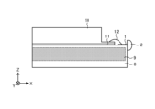
- Embodiment 1. 1 is a schematic diagram showing a laser processing apparatus 100 including a laser device 110 according to a first embodiment.
- the laser processing apparatus 100 processes a workpiece 140 by irradiating the workpiece 140 with a laser beam r.
- the processing includes, for example, cutting, welding, and drilling.
- the workpiece 140 is, for example, a metal plate or a substrate.
- the laser processing apparatus 100 includes the laser device 110, a propagation member 120, a processing head 130, and a processing table 150.
- the laser device 110 emits a laser beam r. Details of the laser device 110 will be described later.
- the propagation member 120 propagates the laser beam r emitted from the laser device 110.
- the laser beam r emitted from the laser device 110 is propagated to the processing head 130 via the propagation member 120.
- the propagation member 120 is, for example, a beam transmission optical path or an optical fiber.
- the processing head 130 focuses the laser beam r propagated from the propagation member 120 and irradiates it onto the workpiece 140.
- the workpiece 140 irradiated with the laser beam r is burned, melted, or sublimated. As a result, the workpiece 140 is subjected to processing such as cutting, welding, and drilling.
- the processing table 150 holds the workpiece 140 and also plays a role in moving the position of the workpiece 140.
- the processing table 150 holds the workpiece 140 by, for example, adsorbing the workpiece 140.
- the processing table 150 is movable, for example, in two axial directions, and is capable of moving the workpiece 140 in the two axial directions.
- the configuration of the laser processing device 100 shown in the figure is one example and may be modified as appropriate.
- the laser device 110 may be applied to a 3D printer or the like by combining it with a commonly known laser processing device.
- FIG. 2 is a schematic diagram showing the laser device 110 according to the first embodiment.
- FIG. 3 is a schematic diagram showing the laser device 110 according to the first embodiment, as viewed along the Y-axis direction in FIG. 2.
- FIG. 4 is a perspective view for explaining the function of the first fast-axis collimating lens 2 and the slow-axis collimating lens 3 according to the first embodiment.
- FIG. 5 is a diagram for explaining the function of the first fast-axis collimating lens 2 according to the first embodiment, as viewed along the Y-axis direction in FIG. 4.
- FIG. 6 is a diagram for explaining the function of the slow-axis collimating lens 3 according to the first embodiment, as viewed along the Z-axis direction in FIG. 4.
- the directions will be described according to the X-axis direction, Y-axis direction, and Z-axis direction shown in FIG. 2.
- the X-axis direction, Y-axis direction, and Z-axis direction shown in FIG. 2 are perpendicular to each other.
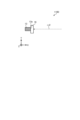
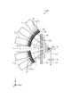
- the laser device 110 includes multiple laser light sources 1, an optical element E, a transmissive diffraction grating 5, and an output coupler 6.
- the laser light source 1 is a member that emits a laser beam r.
- the multiple laser light sources 1 are arranged side by side on the same plane and have multiple light emitting points 1a that emit the laser beam r.
- the laser beam r emitted from each laser light source 1 is drawn with a single line, but in reality, multiple laser beams r are emitted from each of the multiple light emitting points 1a of each laser light source 1.
- the multiple laser light sources 1 are arranged in the XY plane.
- the light emitting point 1a that is located on one side of the first gap 7 described below and closest to the first gap 7 is referred to as light emitting point 1b.
- the light emitting point 1a that is located on the other side of the first gap 7 and closest to the first gap 7 is referred to as light emitting point 1c.
- the light emitting point 1a that is located on one side of the first gap 7 and farthest from the first gap 7 is referred to as light emitting point 1d.
- the light-emitting point 1a located on the other side of the first gap 7 and furthest from the first gap 7 is referred to as light-emitting point 1e.
- the laser beams r emitted from each of the multiple laser light sources 1 overlap at a position away from each laser light source 1.
- the laser beams r overlap on the transmission type diffraction grating 5.
- the position where the laser beams r overlap is referred to as the overlapping position S.
- the overlapping of the laser beams r on the transmission type diffraction grating 5 includes a state where the laser beams r overlap at one point on the transmission type diffraction grating 5, as well as a state where the laser beams r are close to each other on the transmission type diffraction grating 5.
- the close state refers to a state where the laser beams r are close enough to each other that the primary light of each laser beam r can be overlapped on the same axis by the diffraction of each laser beam r in the transmission type diffraction grating 5.
- the multiple laser light sources 1 are arranged on one arc centered on the overlapping position S, but they may also be arranged on approximately one arc centered on the overlapping position S.
- the arrangement on approximately one arc means that a certain error is allowed in the arrangement of the laser light sources 1.
- the range of the certain error means a range in which the effect of this disclosure can be achieved.
- the position of the laser light source 1 may deviate from one arc centered on the overlapping position S as long as the laser beam r having the necessary characteristics can be obtained by superimposing the laser beams r emitted from each of the multiple light emitting points 1a for the purpose of laser processing such as cutting and welding. Therefore, even if there is a deviation of the laser light source 1 due to the requirements of the optical design, a processing tolerance that occurs during the manufacture of the product, or a deviation of the laser light source 1 due to the arrangement work, it is considered to be included in the range of approximately one arc. When the change in the output of the laser beam r, the quality of the laser beam r, etc.
- the deviation of the laser light source 1 due to the requirements of the optical design is the deviation of the distance of each laser light source 1 from the overlapping position S that is intentionally set in the optical design in order to equalize the optical operating characteristics of the multiple laser light sources 1.
- the laser light source 1 is a semiconductor laser bar.
- the laser light source 1 shown in FIG. 2 is a semiconductor laser array element having a plurality of light emitting points 1a that emit a laser beam r.
- the number of light emitting points 1a of each laser light source 1 is three in this embodiment, but may be changed as appropriate.
- the laser light sources 1 are arranged on one side and the other side of a first gap 7, which will be described later.
- the number of laser light sources 1 is five in this embodiment, but may be a number other than five. It is sufficient that at least one laser light source 1 is arranged on one side and the other side of the first gap 7.
- a first gap 7 is formed between two adjacent laser light sources 1 among the multiple laser light sources 1.
- the first gap 7 is located on the optical path of the reflected first-order diffracted light r2 emitted from the transmission diffraction grating 5.
- the first gap 7 is formed between the third laser light source 1 from the top of the paper in FIG. 2 and the fourth laser light source 1 from the top of the paper in FIG. 2, but the position of the first gap 7 is changed as appropriate depending on the number of laser light sources 1 and the optical path of the reflected first-order diffracted light r2.
- the virtual line connecting the light emitting point 1b, which is disposed on one side of the first gap 7 and is closest to the first gap 7, and the overlap position S is defined as a virtual line C1.
- the virtual line connecting the light emitting point 1c, which is disposed on the other side of the first gap 7 and is closest to the first gap 7, and the overlap position S is defined as a virtual line C2.
- the first angle ⁇ 1 formed by the virtual lines C1 and C2 is 0.15 degrees or more. In addition, it is preferable that the first angle ⁇ 1 is 1.0 degrees or less.
- the virtual line connecting the light emitting point 1d, which is disposed on one side of the first gap 7 and is farthest from the first gap 7, and the overlap position S is defined as a virtual line C3.
- the virtual line connecting the light emitting point 1e, which is disposed on the other side of the first gap 7 and is farthest from the first gap 7, and the overlap position S is defined as a virtual line C4. It is preferable that the second angle ⁇ 2 formed by the virtual lines C3 and C4 is 5 degrees or more.
- the optical element E is a member that collimates the laser beam r emitted from each of the multiple laser light sources 1.
- the optical element E serves to reduce the variation in the angle of incidence of each laser beam r incident on the transmission diffraction grating 5.
- the optical element E has a plurality of first fast axis collimating lenses 2, a plurality of slow axis collimating lenses 3, and a second fast axis collimating lens 4.
- the first fast axis collimating lens 2, the plurality of slow axis collimating lenses 3, and the second fast axis collimating lens 4 are cylindrical lenses.
- the multiple first fast axis collimating lenses 2 are provided for each of the multiple laser light sources 1 and are members that collimate the laser beam r emitted from each of the multiple laser light sources 1 in the fast axis direction.
- the multiple first fast axis collimating lenses 2 are provided for each of the multiple laser light sources 1.
- the fast axis direction is parallel to the Z axis direction.
- the first fast axis collimating lenses 2 reduce the divergence angle of the laser beam r in the Z axis direction.
- the slow-axis collimating lenses 3 are provided for each of the multiple laser light sources 1, and are components that collimate the laser beam r emitted from each of the multiple first fast-axis collimating lenses 2 in the slow-axis direction.
- the multiple slow-axis collimating lenses 3 are provided for each of the multiple laser light sources 1.
- the slow-axis direction is the direction in which the light-emitting points 1a are lined up in the XY plane.
- the slow-axis direction is illustrated by the arrow Sa.
- the slow-axis collimating lens 3 reduces the divergence angle of the laser beam r in the slow-axis direction.
- the second fast axis collimating lens 4 is a member that collimates the laser beam r emitted from each of the multiple slow axis collimating lenses 3 in the fast axis direction. That is, the second fast axis collimating lens 4 recollimates each laser beam r that has expanded in the fast axis direction after being emitted from each of the multiple slow axis collimating lenses 3 in the fast axis direction.
- the laser beam r emitted from each of the multiple slow axis collimating lenses 3 is incident on the second fast axis collimating lens 4.
- the second fast axis collimating lens 4 like the first fast axis collimating lens 2, reduces the divergence angle of the laser beam r in the Z axis direction.
- the transmission type diffraction grating 5 is a component that coaxially superimposes a portion of the laser beam r emitted from the optical element E and emits the coaxially superimposed laser beam r as transmitted first-order diffracted light r1.
- the transmission type diffraction grating 5 diffracts each of the multiple laser beams r emitted from the optical element E in the XY plane using wavelength dispersion, and separates them into orders.
- the transmission type diffraction grating 5 coaxially superimposes the first-order light of each of the multiple laser beams r and emits it as transmitted first-order diffracted light r1.
- the transmitted first-order diffracted light r1 is emitted toward the output coupler 6.
- the transmission type diffraction grating 5 also emits reflected first-order diffracted light r2 in a direction different from the emission direction of the transmitted first-order diffracted light r1.
- the reflected first-order diffracted light r2 is emitted toward the laser light source 1.
- the transmission diffraction grating 5 is disposed at an overlapping position S where the laser beams r emitted from each of the multiple laser light sources 1 overlap.
- the transmission diffraction grating 5 is tilted in the X-axis direction and the Y-axis direction in the XY plane.
- the laser light source 1 and the transmission diffraction grating 5 are disposed on the same plane in the XY plane.
- the transmission diffraction grating 5 is disposed parallel to a direction perpendicular to the same plane in which the multiple laser light sources 1 are disposed. In this embodiment, the direction perpendicular to the same plane is the Z-axis direction.
- the transmission diffraction grating 5 is disposed parallel to the Z-axis direction.
- the laser light source 1, the first fast axis collimating lens 2, the slow axis collimating lens 3, the second fast axis collimating lens 4, the transmission diffraction grating 5, and the output coupler 6 are disposed on the same plane in the XY plane.
- the output coupler 6 is a component that reflects a portion of the transmitted first-order diffracted light r1 emitted from the transmission grating 5 toward the laser light source 1 and emits the remaining portion of the transmitted first-order diffracted light r1 emitted from the transmission grating 5. In FIG. 2, only the remaining portion of the transmitted first-order diffracted light r1 emitted from the output coupler 6 is shown.
- the output coupler 6 is, for example, a partial reflection mirror.
- the multiple laser light sources 1 and the output coupler 6 form a resonator.
- the laser beam r emitted from the multiple laser light sources 1 is amplified by repeated reflection between the laser light sources 1 and the output coupler 6.
- a portion of the amplified laser beam r is emitted from the output coupler 6 to the outside of the laser device 110 and propagates to the processing head 130 via the propagation member 120 shown in FIG. 1.
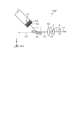
- Figure 7 is a perspective view showing an example of the peripheral configuration of the laser light source 1 according to the first embodiment.
- Figure 8 is a side view showing an example of the peripheral configuration of the laser light source 1 according to the first embodiment.
- a first power supply member 8 As shown in Figures 7 and 8, a first power supply member 8, a second power supply member 10, an insulating plate 11, and an electric wire 12 are arranged around the laser light source 1 and the first fast axis collimating lens 2.
- the first power supply member 8 is a member that supplies power to the laser light source 1.
- the shape of the first power supply member 8 is a rectangular parallelepiped, but may be modified as appropriate.
- the laser light source 1 is installed on one end face of the first power supply member 8 in the Z-axis direction.
- the first fast axis collimating lens 2 is fixed to one end face of the first power supply member 8 in the X-axis direction with an adhesive or the like.
- the first fast axis collimating lens 2 covers the emission surface of the laser light source 1.
- a cooling mechanism 9 for cooling the laser light source 1 is provided inside the first power supply member 8.
- the cooling mechanism 9 is, for example, a cooling water channel through which cooling water flows.
- the second power supply member 10 is a member that supplies power to the laser light source 1.
- the shape of the second power supply member 10 is a rectangular parallelepiped, but may be changed as appropriate.
- the size of the second power supply member 10 is smaller than the size of the first power supply member 8.
- the second power supply member 10 is installed on one end surface of the first power supply member 8 in the Z-axis direction.
- the second power supply member 10 and the laser light source 1 are installed apart from each other in the X-axis direction.
- the second power supply member 10 and the laser light source 1 are electrically connected via a plurality of electric wires 12.
- An insulating plate 11 that electrically insulates the first power supply member 8 and the second power supply member 10 is installed between them. Note that the configuration around the laser light source 1 and the first fast axis collimator lens 2 shown in the figure is an example, and may be changed as appropriate.
- a first gap 7 is formed between two adjacent laser light sources 1 among the multiple laser light sources 1, the first gap 7 being located on the optical path of the reflected first-order diffracted light r2 emitted from the transmission type diffraction grating 5.
- the first angle ⁇ 1 formed by the virtual straight line C1 connecting the light emitting point 1b, which is located on one side of the first gap 7 and closest to the first gap 7, and the overlapping position S, and the virtual straight line C2 connecting the light emitting point 1c, which is located on the other side of the first gap 7 and closest to the first gap 7, and the overlapping position S, is 0.15 degrees or more.
- the reflected first-order diffracted light r2 does not pass through the first gap 7 and is not irradiated to the laser light source 1, so that damage to the laser light source 1 caused by the reflected first-order diffracted light r2 can be suppressed.
- the reflected first-order diffracted light r2 does not pass through the first gap 7 and is not irradiated to the first fast-axis collimating lens 2 and the slow-axis collimating lens 3, so damage to the first fast-axis collimating lens 2 and the slow-axis collimating lens 3 due to the reflected first-order diffracted light r2 can also be suppressed.
- the optical path of the reflected first-order diffracted light r2 changes due to the influence of the positional deviation, angle deviation, etc. of the laser light source 1 and the optical element E. If the first angle ⁇ 1 is 0.15 degrees or more as in this embodiment, even if the optical path of the reflected first-order diffracted light r2 changes due to the influence of the positional deviation, angle deviation, etc., the reflected first-order diffracted light r2 passes through the first gap 7, so that the reflected first-order diffracted light r2 can be prevented from being irradiated to the laser light source 1. On the other hand, if the first angle ⁇ 1 is 1.0 degree or less, the increase in the first gap 7 can be suppressed, and the multiple laser light sources 1 can be arranged compactly, so that the laser device 110 can be prevented from becoming large.
- the first angle ⁇ 1 shown in Figure 2 may be appropriately adjusted.
- the transmission grating 5 is arranged parallel to a direction perpendicular to the same plane on which the multiple laser light sources 1 are arranged.
- the transmitted first-order diffracted light r1 emitted from the transmission grating 5 is less likely to be twisted or tilted, and the quality of the laser beam r emitted from the output coupler 6 can be improved.
- a laser device 110 can be obtained that can suppress damage to the laser light source 1 caused by the reflected first-order diffracted light r2 while suppressing deterioration in the quality of the laser beam r.
- the laser light sources 1 are arranged on both sides of the first gap 7.
- the number of laser light sources 1 can be increased compared to when the laser light sources 1 are arranged on only one side of the first gap 7, and therefore the total output of the laser beam r can be increased.
- the laser light source 1 is a semiconductor laser array element having multiple light emitting points 1a. This configuration makes it possible to achieve high output of the laser beam r of the laser device 110.
- the optical element E has a configuration including a plurality of first fast-axis collimating lenses 2, a plurality of slow-axis collimating lenses 3, and a second fast-axis collimating lens 4.
- This configuration can reduce the variation in the angle of incidence of each laser beam r incident on the transmission diffraction grating 5, thereby improving the utilization efficiency of the laser beam r.
- the configuration of the optical element E described above makes it easier for the reflected first-order diffracted light r2 to be focused toward the laser light source 1, which is a disadvantage in that the reflected first-order diffracted light r2 is more likely to damage the laser light source 1.
- the first gap 7 located on the optical path of the reflected first-order diffracted light r2 is formed, and the first angle ⁇ 1 is 0.15 degrees or more, so that the reflected first-order diffracted light r2 does not pass through the first gap 7 and is not irradiated to the laser light source 1, thereby suppressing damage to the laser light source 1 due to the reflected first-order diffracted light r2.
- the disadvantages of the configuration of the optical element E described above can be eliminated.
- the laser device 110 according to the present embodiment is preferably used to realize high output of the laser beam r in the Wavelength Beam Combining (WBC) technology.
- WBC Wavelength Beam Combining
- the output of the laser beam r emitted from the output coupler 6 is 2 kW or more.
- the number of laser light sources 1 is 12 or more.
- the diffraction angle of the transmitted first-order diffracted light r1 emitted from the transmission type diffraction grating 5 is 60 degrees or more.
- the second angle ⁇ 2 of the laser beam r incident on the transmission diffraction grating 5 is 5 degrees or more.
- the reflected first-order diffracted light r2 has an output equivalent to approximately 1% of the output of the laser beam r emitted from the output coupler 6. According to the applicant's experiments and research, it has been found that when the output of the reflected first-order diffracted light r2 exceeds 20 W, damage to the laser light source 1 and the like becomes apparent. For this reason, it is preferable that the output of the laser beam r emitted from the output coupler 6 is 2 kW or more.
- a laser light source 1 that enables high output suitable for laser processing in the wavelength beam combining technology
- a semiconductor laser bar in which a plurality of light emitting points 1a are integrally formed on a semiconductor chip with a width of 10 mm is useful and common.
- the upper limit of the output of a semiconductor laser bar available on the market is currently about 200 W.
- the output of the laser beam r emitted from the output coupler 6 is reduced by about 20% from the output of the semiconductor laser bar.
- the theoretical limit of the transmission type diffraction grating 5 applicable to the laser beam r having a wavelength of about 980 nm in the near infrared region is a number of grooves of about 2000/mm, and the limit of the number of grooves of about 1850/mm is the number of grooves available on the market.
- the diffraction angle of the transmission type diffraction grating 5 at which the diffraction efficiency of the transmission type diffraction grating 5 is maximized is about 65 degrees.
- the diffraction angle of the transmitted first-order diffracted light r1 emitted from the transmission type diffraction grating 5 is 60 degrees or more.
- the numerical value of the diffraction angle of the transmission type diffraction grating 5 under this condition will be the same even if the wavelength band used is changed to, for example, about 450 nm of a blue laser.
- the incident angle of the laser beam r on the transmission type diffraction grating 5 can be set in the range of 55 degrees to 59 degrees, thereby suppressing the reflected first-order diffracted light r2 from being irradiated onto the laser light source 1 while performing efficient wavelength beam combining.
- the distance between the laser light source 1 and the transmission type diffraction grating 5 needs to be 2 m or more, and considering the size of the laser device 110 for the laser processing device 100, it is difficult to achieve a distance of 2 m or more between the laser light source 1 and the transmission type diffraction grating 5. For this reason, it is preferable that the second angle ⁇ 2 of the laser beam r incident on the transmission type diffraction grating 5 is 5 degrees or more.
- the laser light source 1 shown in FIG. 2 is a semiconductor laser array element, but it may be a semiconductor laser bar other than a semiconductor laser array element.
- the laser light source 1 may be, for example, an edge-emitting semiconductor laser bar having one light-emitting point 1a, or a surface-emitting semiconductor laser bar having one or more light-emitting points 1a.
- the optical element E shown in FIG. 2 has a plurality of first fast axis collimating lenses 2, a plurality of slow axis collimating lenses 3, and a second fast axis collimating lens 4, but the configuration of the optical element E may be changed as appropriate.
- the second fast axis collimating lens 4 may be omitted from the optical element E.
- a laser device 110A according to a second embodiment will be described with reference to Fig. 9.
- Fig. 9 is a schematic diagram showing the laser device 110A according to the second embodiment. This embodiment differs from the first embodiment in that the laser device 110A further includes an output monitor member 13.
- the same reference numerals are used for parts that overlap with the first embodiment, and the description thereof will be omitted.
- the output monitor member 13 is a member that is disposed in the first gap 7 and measures the output fluctuation of the reflected first-order diffracted light r2.
- the output monitor member 13 is, for example, a thermopile sensor.
- the output monitor member 13 has an incident surface 13a on which the reflected first-order diffracted light r2 is incident.
- the incident surface 13a is a flat surface that is parallel to the Z-axis direction and the Y-axis direction.
- the incident surface 13a is a surface that is perpendicular to the optical axis of the reflected first-order diffracted light r2.
- the laser device 110A further includes an output monitor member 13 that is disposed in the first gap 7 and measures the output fluctuation of the reflected first-order diffracted light r2.
- an output monitor member 13 that is disposed in the first gap 7 and measures the output fluctuation of the reflected first-order diffracted light r2.
- the output monitor member 13 may be a photodiode. In this way, the output fluctuation of the reflected first-order diffracted light r2 can be measured at high speed.
- a laser device 110B according to a third embodiment will be described with reference to Fig. 10.
- Fig. 10 is a schematic diagram showing a laser device 110B according to a third embodiment. This embodiment differs from the first and second embodiments in that the laser device 110B further includes a shielding member 14.
- the same reference numerals are used for parts that overlap with the first and second embodiments, and descriptions thereof will be omitted.
- members other than the output monitor member 13 and the shielding member 14 are omitted.
- the shielding member 14 is installed on the output monitor member 13 and surrounds the periphery of the incident surface 13a.
- the shielding member 14 is a cylindrical member that extends along the periphery of the incident surface 13a.
- the shielding member 14 serves to block light M that is incident obliquely on the incident surface 13a of the output monitor member 13.
- the light M that is incident obliquely is scattered light around the output monitor member 13, and is light that is not the object of measurement for the output monitor member 13.
- the laser device 110B further includes a shielding member 14 that is installed on the output monitor member 13 and surrounds the periphery of the incident surface 13a.
- This configuration can block light M that is obliquely incident on the incident surface 13a of the output monitor member 13, thereby improving the measurement accuracy of the output fluctuation of the reflected first-order diffracted light r2.
- a laser device 110C according to a fourth embodiment will be described with reference to Fig. 11.
- Fig. 11 is a schematic diagram showing a laser device 110C according to a fourth embodiment. This embodiment differs from the first to third embodiments in that the laser device 110C further includes an object-side telecentric lens 15.
- the same reference numerals are used for parts that overlap with the first to third embodiments, and descriptions thereof will be omitted.
- members other than the output monitor member 13 and the object-side telecentric lens 15 are omitted.
- the object-side telecentric lens 15 is a member that is installed on the incident surface 13a of the output monitor member 13 and transmits only the reflected first-order diffracted light r2 that is perpendicularly incident on the incident surface 13a.
- the object-side telecentric lens 15 serves to cut off the light M that is obliquely incident on the incident surface 13a.
- the laser device 110C further includes an object-side telecentric lens 15 that is installed on the incident surface 13a of the output monitor member 13 and transmits only the reflected first-order diffracted light r2 that is perpendicularly incident on the incident surface 13a.
- This configuration makes it possible to cut off the light M that is obliquely incident on the incident surface 13a of the output monitor member 13, thereby improving the measurement accuracy of the output fluctuation of the reflected first-order diffracted light r2.
- a laser device 110D according to a fifth embodiment will be described with reference to Fig. 12.
- Fig. 12 is a schematic diagram showing a laser device 110D according to a fifth embodiment. This embodiment differs from the first to fifth embodiments in that the laser device 110D further includes a light-attenuating optical element 16.
- the same reference numerals are used for parts that overlap with the first to fourth embodiments, and the description thereof will be omitted.
- members other than the output monitor member 13 and the light-attenuating optical element 16 are omitted.
- the dimming optical element 16 is a member that is placed between the incident surface 13a of the output monitor member 13 and the transmission type diffraction grating 5 shown in FIG. 9, and attenuates the light intensity of the reflected first-order diffracted light r2 that is incident on the output monitor member 13.
- the dimming optical element 16 is placed ahead of the second fast axis collimator lens 4 shown in FIG. 9 in the traveling direction of the reflected first-order diffracted light r2.
- the dimming optical element 16 is placed on the incident surface 13a of the output monitor member 13.
- the dimming optical element 16 is, for example, an ND (Neutral Density) filter or a partial reflection mirror.
- the laser device 110D further includes a dimming optical element 16 that is disposed between the incident surface 13a of the output monitor member 13 and the transmission type diffraction grating 5 and attenuates the light intensity of the reflected first-order diffracted light r2 incident on the output monitor member 13.
- a dimming optical element 16 that is disposed between the incident surface 13a of the output monitor member 13 and the transmission type diffraction grating 5 and attenuates the light intensity of the reflected first-order diffracted light r2 incident on the output monitor member 13.
- the output monitor member 13 When a photodiode with a lower upper limit of the amount of incident light compared to a thermopile sensor or the like is used as the output monitor member 13, it is advisable to use the photodiode in combination with the dimming optical element 16. In this way, the amount of reflected first-order diffracted light r2 can be attenuated by the dimming optical element 16 before the reflected first-order diffracted light r2 enters the photodiode. Therefore, the output fluctuation of the reflected first-order diffracted light r2 can be appropriately measured by the photodiode.
- the dimming optical element 16 may be used in combination with the object-side telecentric lens 15 shown in FIG. 11. In such a configuration, it is preferable to arrange the dimming optical element 16, the object-side telecentric lens 15, and the output monitor member 13 in this order along the traveling direction of the reflected first-order diffracted light r2. In other words, it is preferable to install the dimming optical element 16 on the entrance surface 13a of the output monitor member 13 via the object-side telecentric lens 15.
- a laser device 110E according to a sixth embodiment will be described with reference to Fig. 13.
- Fig. 13 is a schematic diagram showing a laser device 110E according to the sixth embodiment. This embodiment differs from the first to fifth embodiments in that the laser device 110E further includes a damper 17.
- the same reference numerals are used for parts that overlap with the first to fifth embodiments, and descriptions thereof will be omitted.
- the damper 17 is a member that is disposed in the first gap 7 and absorbs the reflected first-order diffracted light r2.
- the laser device 110E further includes a damper 17 disposed in the first gap 7 to absorb the reflected first-order diffracted light r2.
- This configuration can suppress the generation of stray light due to the reflected first-order diffracted light r2, and can also suppress heating of components in the laser device 110E due to the reflected first-order diffracted light r2.
- a laser device 110F according to the seventh embodiment will be described with reference to Figs. 14 and 15.
- Fig. 14 is a schematic diagram showing the laser device 110F according to the seventh embodiment.
- Fig. 15 is a schematic diagram showing the laser device 110F according to the seventh embodiment, as viewed along the Y-axis direction in Fig. 14.
- This embodiment differs from the first to sixth embodiments in that the laser light source 1, the first fast-axis collimating lens 2, the slow-axis collimating lens 3, the second fast-axis collimating lens 4, the transmission grating 5, and the output coupler 6 are not arranged on the same plane, and the laser device 110F further includes a mirror 18.
- the same reference numerals are used for the parts that overlap with the first to sixth embodiments, and the description thereof will be omitted.
- the laser light source 1, the first fast axis collimating lens 2, and the slow axis collimating lens 3 are arranged offset in the Z-axis direction, which is a direction perpendicular to the second fast axis collimating lens 4, the transmission diffraction grating 5, and the output coupler 6.
- the laser light source 1, the first fast axis collimating lens 2, and the slow axis collimating lens 3 are tilted with respect to the Z-axis direction.
- the optical axis of the laser beam r emitted from each of the laser light source 1, the first fast axis collimating lens 2, and the slow axis collimating lens 3 is tilted with respect to the Z-axis direction.
- the mirror 18 is disposed between the slow axis collimating lens 3 and the second fast axis collimating lens 4.
- the mirror 18 reflects the laser beam r emitted from the slow axis collimating lens 3 toward the second fast axis collimating lens 4.
- the mirror 18 is inclined so as to move away from the slow axis collimating lens 3 in the Z-axis direction as it moves from the slow axis collimating lens 3 toward the second fast axis collimating lens 4.
- the mirror 18 is divided into two in a direction intersecting the optical axis of the laser beam r emitted from each of the multiple slow-axis collimating lenses 3.
- the mirror 18 is divided into two in the Y-axis direction.
- a second gap 19 is formed that is located on the optical path of the reflected first-order diffracted light r2.
- the first gap 7 and the second gap 19 are aligned in the Y-axis direction.
- the first gap 7 and the second gap 19 are misaligned in the X-axis direction and the Z-axis direction.
- the laser light source 1, the first fast axis collimating lens 2, and the slow axis collimating lens 3 are arranged to be shifted in the Z-axis direction with respect to the second fast axis collimating lens 4, the transmission type diffraction grating 5, and the output coupler 6.
- the laser device 110F further includes a mirror 18 arranged between the slow axis collimating lens 3 and the second fast axis collimating lens 4 to reflect the laser beam r emitted from the slow axis collimating lens 3 toward the second fast axis collimating lens 4.
- FIG. 1 the laser light source 1
- the slow axis collimating lens 2 the slow axis collimating lens 3
- the transmission type diffraction grating 5 the output coupler 6.
- the laser device 110F further includes a mirror 18 arranged between the slow axis collimating lens 3 and the second fast axis collimating lens 4 to reflect the laser beam r emitted from the slow axis collimating lens 3 toward the
- the mirror 18 is divided into two, and a second gap 19 is formed between the two adjacent mirrors 18, which is located on the optical path of the reflected first-order diffracted light r2.
- the reflected first-order diffracted light r2 passes through a position shifted from the laser light source 1 in the Z-axis direction, so that the reflected first-order diffracted light r2 can be prevented from being irradiated onto the laser light source 1. This makes it possible to suppress damage to the laser light source 1 caused by the reflected first-order diffracted light r2.
- the output monitor member 13 or the damper 17 When the output monitor member 13 or the damper 17 is installed, the output monitor member 13 or the damper 17 is installed ahead of the second gap 19 in the traveling direction of the reflected first-order diffracted light r2. With this configuration, the reflected first-order diffracted light r2 emitted from the transmission type diffraction grating 5 passes through the second gap 19 and then enters the output monitor member 13 or the damper 17. Therefore, even if a mirror 18 is provided, it becomes easy to monitor the output fluctuation of the reflected first-order diffracted light r2 by the output monitor member 13, and it becomes easy to absorb the reflected first-order diffracted light r2 by the damper 17.
- the laser light source 1 the first fast axis collimating lens 2, and the slow axis collimating lens 3 so that they are not shifted in the Z-axis direction, which is the direction perpendicular to the second fast axis collimating lens 4, the transmission type diffraction grating 5, and the output coupler 6.
- a laser device 110G according to an eighth embodiment will be described with reference to Fig. 16 and Fig. 17.
- Fig. 16 is a schematic diagram showing the laser device 110G according to the eighth embodiment.
- Fig. 17 is a perspective view showing the beam rotation element 20 of the laser device 110G according to the eighth embodiment.
- This embodiment differs from the first to seventh embodiments in that the laser device 110G further includes a beam rotation element 20.
- the same reference numerals are used for parts that overlap with the first to seventh embodiments, and description thereof will be omitted.
- the beam rotation element 20 is disposed between the first fast axis collimating lens 2 and the slow axis collimating lens 3.
- the beam rotation element 20 serves to rotate the laser beam r by 90 degrees around the optical axis of the laser beam r.
- the beam rotation element 20 is a rotation optical system that rotates an image by 90 degrees around the optical axis of the laser beam r.
- the beam rotation element 20 shown in FIG. 17 is a lens array having multiple lenses.
- the surface of the beam rotation element 20 facing the first fast axis collimating lens 2 and the surface facing the opposite side to the first fast axis collimating lens 2 each have a plurality of cylindrical surfaces arranged in one direction. Each cylindrical surface is convex. Each cylindrical surface is tilted 45 degrees with respect to a vertical axis Va perpendicular to the horizontal axis Ha.
- the arrangement pitch of the multiple lenses is the same as the arrangement pitch of the multiple light emitting points 1a in the laser light source 1. If the focal length due to refraction on the cylindrical surface is f, the distance L between the cylindrical surface facing the first fast axis collimating lens 2 and the cylindrical surface facing the opposite side to the first fast axis collimating lens 2 is 2f.
- the long axis direction of the incident light which is the laser beam r that enters the beam rotation element 20 from the first fast axis collimating lens 2 is the direction of the vertical axis Va.
- the short axis direction of the incident light is the direction of the horizontal axis Ha.
- the long axis direction of the outgoing light which is the laser beam r that enters the beam rotation element 20 from the first fast axis collimating lens 2 and then exits the beam rotation element 20, is the direction of the horizontal axis Ha.
- the short axis direction of the outgoing light is the direction of the vertical axis Va.
- the beam rotation element 20 emits outgoing light whose long axis and short axis directions are swapped with those of the incident light. In this way, the beam rotation element 20 rotates the laser beam r by 90 degrees around the optical axis of the laser beam r.
- the total angle of the divergence angle of the laser beam r in the slow axis direction is generally about 5 degrees to 10 degrees, whereas the total angle of the divergence angle of the laser beam r in the fast axis direction is about 30 degrees to 60 degrees.
- the divergence angle of the laser beam r in the fast axis direction is larger than the divergence angle of the laser beam r in the slow axis direction.
- the focusing performance of the semiconductor laser bar in the slow axis direction is lower than the focusing performance of the semiconductor laser bar in the fast axis direction.
- BPP Beam Parameter Product
- BPP Beam Parameter Product
- the unit of BPP is expressed in mm mrad.
- a deformation called a smile may occur in the semiconductor laser bar. Due to the smile, the positions of the multiple light emitting points 1a vary in the fast axis direction. According to this embodiment, the beam rotation element 20 rotates the laser beam r by 90 degrees around the optical axis of the laser beam r, so that the direction in which the position of the light emitting points 1a varies due to the smile is converted to the slow axis direction, in which the focusing performance is relatively poor. This makes it possible to reduce the deterioration of the focusing performance caused by the smile.
- the first fast axis collimating lens 2 when a first fast axis collimating lens 2 made of a lens having a cylindrical surface is used, the first fast axis collimating lens 2 is installed at a slight inclination with respect to the XY plane, so that the laser beam r is emitted from the first fast axis collimating lens 2 with an angle in the Z axis direction.
- a beam rotation element 20 is installed immediately after the first fast axis collimating lens 2
- the laser beam r is converted from an angled state in the Z axis direction to an angled state in the XY plane by passing through the beam rotation element 20.
- the laser beams r can be brought closer to each other while traveling toward the transmission type diffraction grating 5.
Landscapes
- Physics & Mathematics (AREA)
- Electromagnetism (AREA)
- Optics & Photonics (AREA)
- Engineering & Computer Science (AREA)
- Plasma & Fusion (AREA)
- Condensed Matter Physics & Semiconductors (AREA)
- General Physics & Mathematics (AREA)
- Semiconductor Lasers (AREA)
- Laser Beam Processing (AREA)
Priority Applications (2)
| Application Number | Priority Date | Filing Date | Title |
|---|---|---|---|
| PCT/JP2023/025727 WO2025013243A1 (ja) | 2023-07-12 | 2023-07-12 | レーザ装置およびレーザ加工装置 |
| JP2023565635A JP7412662B1 (ja) | 2023-07-12 | 2023-07-12 | レーザ装置およびレーザ加工装置 |
Applications Claiming Priority (1)
| Application Number | Priority Date | Filing Date | Title |
|---|---|---|---|
| PCT/JP2023/025727 WO2025013243A1 (ja) | 2023-07-12 | 2023-07-12 | レーザ装置およびレーザ加工装置 |
Publications (1)
| Publication Number | Publication Date |
|---|---|
| WO2025013243A1 true WO2025013243A1 (ja) | 2025-01-16 |
Family
ID=89451959
Family Applications (1)
| Application Number | Title | Priority Date | Filing Date |
|---|---|---|---|
| PCT/JP2023/025727 Pending WO2025013243A1 (ja) | 2023-07-12 | 2023-07-12 | レーザ装置およびレーザ加工装置 |
Country Status (2)
| Country | Link |
|---|---|
| JP (1) | JP7412662B1 (https=) |
| WO (1) | WO2025013243A1 (https=) |
Families Citing this family (2)
| Publication number | Priority date | Publication date | Assignee | Title |
|---|---|---|---|---|
| CN118137292A (zh) * | 2024-03-13 | 2024-06-04 | 武汉锐科光纤激光技术股份有限公司 | 半导体激光器和激光装置 |
| CN120657547A (zh) * | 2024-03-15 | 2025-09-16 | 华为技术有限公司 | 激光器及激光设备 |
Citations (6)
| Publication number | Priority date | Publication date | Assignee | Title |
|---|---|---|---|---|
| JP2000091670A (ja) * | 1998-09-07 | 2000-03-31 | Nec Corp | 固体レーザ発生装置 |
| JP2007225989A (ja) * | 2006-02-24 | 2007-09-06 | Ricoh Co Ltd | マルチビーム光源ユニット、それを備えた光走査装置および画像形成装置 |
| JP2011205061A (ja) * | 2010-03-04 | 2011-10-13 | Komatsu Ltd | レーザ装置、レーザシステムおよび極端紫外光生成装置 |
| US20190214786A1 (en) * | 2018-01-09 | 2019-07-11 | Daylight Solutions, Inc. | Laser assembly with spectral beam combining |
| JP2021524161A (ja) * | 2018-05-22 | 2021-09-09 | パナソニックIpマネジメント株式会社 | 波長合成技術用レーザシステムにおけるパワー及びスペクトラムのモニタリング |
| JP2022508765A (ja) * | 2018-10-15 | 2022-01-19 | パナソニックIpマネジメント株式会社 | 階段状スロー軸コリメータを有するレーザシステム |
-
2023
- 2023-07-12 WO PCT/JP2023/025727 patent/WO2025013243A1/ja active Pending
- 2023-07-12 JP JP2023565635A patent/JP7412662B1/ja active Active
Patent Citations (6)
| Publication number | Priority date | Publication date | Assignee | Title |
|---|---|---|---|---|
| JP2000091670A (ja) * | 1998-09-07 | 2000-03-31 | Nec Corp | 固体レーザ発生装置 |
| JP2007225989A (ja) * | 2006-02-24 | 2007-09-06 | Ricoh Co Ltd | マルチビーム光源ユニット、それを備えた光走査装置および画像形成装置 |
| JP2011205061A (ja) * | 2010-03-04 | 2011-10-13 | Komatsu Ltd | レーザ装置、レーザシステムおよび極端紫外光生成装置 |
| US20190214786A1 (en) * | 2018-01-09 | 2019-07-11 | Daylight Solutions, Inc. | Laser assembly with spectral beam combining |
| JP2021524161A (ja) * | 2018-05-22 | 2021-09-09 | パナソニックIpマネジメント株式会社 | 波長合成技術用レーザシステムにおけるパワー及びスペクトラムのモニタリング |
| JP2022508765A (ja) * | 2018-10-15 | 2022-01-19 | パナソニックIpマネジメント株式会社 | 階段状スロー軸コリメータを有するレーザシステム |
Also Published As
| Publication number | Publication date |
|---|---|
| JPWO2025013243A1 (https=) | 2025-01-16 |
| JP7412662B1 (ja) | 2024-01-12 |
Similar Documents
| Publication | Publication Date | Title |
|---|---|---|
| JP7277716B2 (ja) | 光源装置、ダイレクトダイオードレーザ装置、および光結合器 | |
| JP7412662B1 (ja) | レーザ装置およびレーザ加工装置 | |
| US11287574B2 (en) | Optical fiber bundle with beam overlapping mechanism | |
| JP7126137B2 (ja) | 波長合成技術用レーザシステムにおけるパワー及びスペクトラムのモニタリング | |
| JP7296605B2 (ja) | 波長ビーム結合共振器のアライメントのためのシステムおよび方法 | |
| JP7153862B2 (ja) | 階段状スロー軸コリメータを有するレーザシステム | |
| JP7212274B2 (ja) | 光源装置、ダイレクトダイオードレーザ装置 | |
| JP2016224376A (ja) | レーザ装置 | |
| JP2024525778A (ja) | 波長ビーム結合レーザーシステム用シングルエミッタスタッキング | |
| JP2022508765A5 (https=) | ||
| WO2021145205A1 (ja) | レーザ装置及びそれを用いたレーザ加工装置 | |
| US12546959B2 (en) | Optical apparatus, light source apparatus, and optical fiber laser | |
| JP2023088438A (ja) | 波長ビーム結合装置、ダイレクトダイオードレーザ装置、およびレーザ加工機 | |
| WO2021145358A1 (ja) | レーザ加工装置 | |
| JP7398649B2 (ja) | レーザ加工装置およびレーザ加工方法 | |
| JPWO2025013243A5 (https=) | ||
| JP7847440B2 (ja) | 光学装置および光源装置 | |
| JP2025022340A (ja) | レーザ発振器及びそれを備えたレーザ加工装置 | |
| JP6949289B1 (ja) | レーザ装置 | |
| JP7098090B1 (ja) | レーザ装置およびレーザ加工機 | |
| WO2021157546A1 (ja) | レーザ加工装置 | |
| US20260024959A1 (en) | Wavelength beam combining device, direct diode laser device, and laser processing machine | |
| JP7377932B1 (ja) | ビーム結合装置及びレーザ加工機 | |
| US20240399496A1 (en) | Wavelength beam combining device, direct diode laser device, and laser processing machine | |
| TWI893654B (zh) | 雷射加工裝置 |
Legal Events
| Date | Code | Title | Description |
|---|---|---|---|
| WWE | Wipo information: entry into national phase |
Ref document number: 2023565635 Country of ref document: JP |
|
| 121 | Ep: the epo has been informed by wipo that ep was designated in this application |
Ref document number: 23945118 Country of ref document: EP Kind code of ref document: A1 |