WO2025009103A1 - リニアモータ制御装置 - Google Patents
リニアモータ制御装置 Download PDFInfo
- Publication number
- WO2025009103A1 WO2025009103A1 PCT/JP2023/024939 JP2023024939W WO2025009103A1 WO 2025009103 A1 WO2025009103 A1 WO 2025009103A1 JP 2023024939 W JP2023024939 W JP 2023024939W WO 2025009103 A1 WO2025009103 A1 WO 2025009103A1
- Authority
- WO
- WIPO (PCT)
- Prior art keywords
- carrier signal
- signal generating
- linear motor
- carrier
- circuits
- Prior art date
- Legal status (The legal status is an assumption and is not a legal conclusion. Google has not performed a legal analysis and makes no representation as to the accuracy of the status listed.)
- Ceased
Links
Images



Classifications
-
- H—ELECTRICITY
- H02—GENERATION; CONVERSION OR DISTRIBUTION OF ELECTRIC POWER
- H02P—CONTROL OR REGULATION OF ELECTRIC MOTORS, ELECTRIC GENERATORS OR DYNAMO-ELECTRIC CONVERTERS; CONTROLLING TRANSFORMERS, REACTORS OR CHOKE COILS
- H02P25/00—Arrangements or methods for the control of AC motors characterised by the kind of AC motor or by structural details
- H02P25/02—Arrangements or methods for the control of AC motors characterised by the kind of AC motor or by structural details characterised by the kind of motor
- H02P25/06—Linear motors
-
- H—ELECTRICITY
- H02—GENERATION; CONVERSION OR DISTRIBUTION OF ELECTRIC POWER
- H02P—CONTROL OR REGULATION OF ELECTRIC MOTORS, ELECTRIC GENERATORS OR DYNAMO-ELECTRIC CONVERTERS; CONTROLLING TRANSFORMERS, REACTORS OR CHOKE COILS
- H02P29/00—Arrangements for regulating or controlling electric motors, appropriate for both AC and DC motors
- H02P29/50—Reduction of harmonics
-
- H—ELECTRICITY
- H02—GENERATION; CONVERSION OR DISTRIBUTION OF ELECTRIC POWER
- H02P—CONTROL OR REGULATION OF ELECTRIC MOTORS, ELECTRIC GENERATORS OR DYNAMO-ELECTRIC CONVERTERS; CONTROLLING TRANSFORMERS, REACTORS OR CHOKE COILS
- H02P2207/00—Indexing scheme relating to controlling arrangements characterised by the type of motor
- H02P2207/07—Doubly fed machines receiving two supplies both on the stator only wherein the power supply is fed to different sets of stator windings or to rotor and stator windings
Definitions
- This disclosure relates to a linear motor control device.
- control signals with a phase difference of 180 degrees are output to multiple inverters, and approximately half of the inverters are operated with the same phase control signal and the remaining half with the opposite phase control signal.
- a phase control unit determines the phases of N carrier signals supplied to multiple inverters that control multiple motors, respectively, so that the sum of N vectors represented by the amount of noise for each of the N motors is zero, thereby suppressing the peak value of the noise current.
- the phase control unit performs calculations so that the sum of N vectors represented by the amount of noise for each of the N motors becomes zero, so the calculation load increases as the number of motors increases.
- This disclosure discloses technology to solve the problems described above, and aims to enable noise suppression in a linear motor control device that has multiple stator windings and multiple corresponding inverters, by operating the multiple inverters at different phases using a simple phase control device.
- the linear motor control device of the present disclosure includes: A linear motor control device that controls a linear motor having N stator windings (N is a natural number equal to or greater than 2), N inverters for supplying power to the corresponding N stator windings; N PWM signal generating units each generating a PWM signal for operating the inverter and supplying the generated PWM signal to each of the N corresponding inverters; n (n is a natural number between 2 and N) carrier signal generating circuits that generate carrier signals used to generate the PWM signal; a phase control unit for controlling a phase of the carrier signal,
- the phase control unit includes: a clock circuit that outputs a synchronization signal; and n counter circuits that receive the synchronization signal and output timing signals to the n corresponding carrier signal generating circuits at times that are different from the time of reception by at least two or more preset times, each of the n carrier signal generating circuits outputs the carrier signal having a preset period when receiving a timing signal from the corresponding counter circuit
- the present disclosure it is possible to control multiple inverters to operate at different phases, and the generated noise currents will also be of different phases, making it possible to suppress an increase in noise current caused by noise currents overlapping in the same phase.
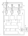
- FIG. 1 is a block diagram showing a configuration of a linear motor system including a linear motor control device according to a first embodiment
- 1 is a block diagram showing a configuration of a linear motor control device according to a first embodiment
- FIG. 2 is a diagram for explaining carrier signals having different phases.
- 13 is a diagram for explaining the relationship between a carrier signal generating circuit and a PWM signal generating unit in a linear motor control device according to a third embodiment.
- FIG. 13 is a diagram for explaining carrier signals having opposite phases to each other in a linear motor control device according to embodiment 4.
- FIG. FIG. 1 is a conceptual diagram showing the phase relationship between in-phase PWM signals and noise generated from an inverter, which is a comparative example.
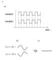
- FIG. 11 is a conceptual diagram showing the phase relationship between the opposite-phase PWM signals and the noise generated from the inverter in a linear motor control device according to embodiment 4, in which (a) shows the waveforms of PWM signals 1 and 2, (b) shows the noise current waveform generated from the inverter operated by PWM signals 1 and 2, and (c) shows the combined noise current.
- 1A and 1B are diagrams illustrating a state in which a generated noise current flows to a reference ground.
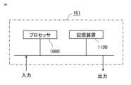
- FIG. 1 is a diagram showing an example of a hardware configuration of an inverter control device of a linear motor control device according to first to fourth embodiments.
- FIG. 1 is a block diagram showing a schematic configuration of a linear motor system including a linear motor control device according to a first embodiment
- FIG. 2 is a functional block diagram showing the configuration of the linear motor control device.
- the linear motor system includes a linear motor 200 and a linear motor control device 100 for driving the linear motor 200 .
- the linear motor 200 generates a magnetic force by passing current through the stator windings 20, and the mover 22 equipped with a permanent magnet is driven along a guide rail 23. Therefore, no power cable is required for the mover 22.
- the multiple stator windings 20 are housed in a housing 24. Power is supplied to each stator winding 20 from the linear motor control device 100 via a power cable 21.
- the number of stator windings 20 is N, which is the same as the number of inverters 1 described below.
- a linear motor control device 100 includes a plurality of N inverters 1 (N is a natural number of 2 or more) each supplying power to a stator winding 20 of a linear motor 200 via a power cable 21, a PWM (Pulse Width Modulation) signal generating unit 10 that generates a PWM signal Pw and transmits it to the inverters 1, a carrier signal generating unit 12 that generates a carrier signal Cw and transmits it to the PWM signal generating unit 10, and a phase control unit 11 that generates a timing signal Tm and transmits it to the carrier signal generating unit 12.
- the PWM signal generating unit 10, the carrier signal generating unit 12, and the phase control unit 11 constitute an inverter control device 101.
- Each of the N inverters 1_1, 1_2, ..., 1_N (collectively referred to as inverter 1) is a single-phase inverter circuit made of a circuit that performs power conversion among the components necessary to realize the inverter function, such as a semiconductor switching element.
- the N inverters 1 are each supplied with power from a common power supply circuit, but the power supply circuit, rectifier circuit, power cable, etc. are not shown.
- the semiconductor switching element is, for example, an element represented by a MOSFET (Metal-Oxide-Semiconductor Field-Effect Transistor) or an IGBT (Insulated-Gate-Bipolar-Transistor).
- These semiconductor switching elements may be formed of a semiconductor made of silicon (Si), or may be a wide bandgap semiconductor formed of a semiconductor material having a wider bandgap than silicon (Si), such as silicon carbide (SiC) or gallium nitride (GaN).
- Si silicon carbide
- GaN gallium nitride
- Each of the inverters 1_1, 1_2, . . . , 1_N corresponds to a respective stator winding 20 of the linear motor 200 and is electrically connected via a power cable 21.
- PWM signal generating units 10_1, 10_2, ..., 10_N (collectively referred to as PWM signal generating units 10) is N, which is the same as the number of inverters 1.
- PWM signals Pw are transmitted from the PWM signal generating units 10_1, 10_2, ..., 10_N corresponding to the inverters 1_1, 1_2, ..., 1_N, respectively.
- Each PWM signal generating unit 10 includes a command signal generating unit 3 and a comparator 2.
- the command signal generating unit 3_1 generates a command signal Sc based on a signal from the control unit 7 and transmits it to the comparator 2_1.
- the comparator 2_1 compares the command signal Sc with a carrier signal Cw generated by the carrier signal generating circuit 4_1, and generates a PWM signal Pw.
- the carrier signal Cw is, for example, a triangular wave having a preset period T.
- control unit 7 determines the current value to be passed through each stator winding 20 based on a command from the higher-level device 110.
- a command signal Sc is generated in the command signal generating unit 3 based on the calculation results in the control unit 7 inside the linear motor control device 100.
- This command signal Sc is a voltage command signal for setting the switching operation of the inverter 1 corresponding to the stator winding 20. Note that the control unit 7 does not necessarily have to be provided within the linear motor control device 100.
- the carrier signal generating unit 12 includes n carrier signal generating circuits 4_1, 4_2, ..., 4_n (collectively referred to as carrier signal generating circuits 4), where n is a natural number satisfying 2 ⁇ n ⁇ N.
- the phase of each carrier signal Cw generated by the carrier signal generating circuit 4 is determined by a timing signal Tm transmitted from the phase control unit 11.
- the phase control unit 11 includes a number n of counter circuits 5_1, 5_2, ... 5_n (collectively referred to as counter circuits 5) and a clock circuit 6.
- the number of carrier signal generating circuits 4 and counter circuits 5 is the same.
- n is greater than the number of inverters N, there will be a surplus of carrier signal generating circuits, so such cases are also excluded. Therefore, candidates for the natural number n are limited to 2 or more and N or less.
- Each of the counter circuits 5_1, 5_2, ... 5_n is a digital circuit that has the function of outputting a timing signal Tm after a preset time t1, t2 ... tn has elapsed from the time t0 when the synchronization signal CLK generated by the clock circuit 6 is received.
- the synchronization signal CLK is an electrical signal that determines the operation start timing of the counter circuit 5 and has the function of synchronizing the operation of the counter circuit 5. The specific form of the signal does not matter, but it is common to use a repeating electrical signal with an arbitrary frequency.
- the synchronization signal CLK is common to all the counter circuits 5.
- the timing signal Tm can be in any form as long as it is an electrical signal, but for example, it is something that outputs a digital signal fixed to 1 (high) or 0 (low) for a certain period of time.
- the specific configuration of the clock circuit 6 is also not important, but it is usually composed of a quartz oscillator and peripheral circuits. There is no need to prepare a clock circuit 6 dedicated to the phase control unit 11, and a clock circuit used in other circuits may be used in combination.
- the carrier signal generating circuit 4 and counter circuit 5 shown here may be configured as discrete components, but may also be implemented in a programmable logic device such as an FPGA (Field Programmable Gate Array).
- the count circuits 5_1, 5_2, ..., 5_n are connected one-to-one to the corresponding carrier signal generating circuits 4_1, 4_2, ..., 4_n, respectively, and supply a timing signal Tm.
- the carrier signal generating circuits 4_1, 4_2, ..., 4_n start outputting a carrier signal Cw with a period T when they receive a timing signal Tm from the count circuits 5_1, 5_2, ..., 5_n.
- the count circuits 5_1, 5_2, ..., 5_n have the function of determining the relative phases of the n different carrier signals Cw.
- FIG. 3 shows carrier signals with different phases.
- the carrier signals generated at two times tk and tl which are arbitrarily selected in advance after receiving the synchronization signal CLK from the clock circuit 6, are designated as carrier signals Cw_k and Cw_l, respectively.
- the times t1, t2, ... tn such that the value of tk-tl is not an integer multiple (including negative numbers) of the period T of the carrier signal, it is possible to generate carrier signals Cw with up to n different phases.
- "different phases" has the meaning described above.
- any of the preset times t1, t2, ... tn prefferably have the same value after receiving the synchronization signal CLK from the clock circuit 6, but because a duplicate number of carrier signals Cw are supplied at that time, the number of carrier signals Cw with different phases is reduced. Therefore, times t1, t2, ... tn are different by at least two or more times.
- the number n of the counter circuits 5 and the carrier signal generating circuits 4 is set to be the same as the number N of the inverters 1, and the above-mentioned times t1, t2 ..., tn are all set to be different.
- the timing signal Tm set in this way is transmitted from the counter circuit 5_k, and based on the carrier signal Cw supplied by the carrier signal generating circuit 4_k that has received this timing signal Tm, the PWM signal generating unit 10_k outputs the PWM signal Pw to the inverter 1_k. Since the N inverters 1_1, 1_2, ..., 1_N of the linear motor control device 100 can all be operated with different phases, it is possible to avoid the problem of noise currents occurring at the same time and their peak values becoming large.
- the linear motor control device is a linear motor control device that controls a linear motor having N (N is a natural number greater than or equal to 2) stator windings, and is equipped with N inverters that supply power to the corresponding N stator windings, N PWM signal generating units that generate PWM signals to operate the inverters and supply them to each of the corresponding N inverters, n (n is a natural number greater than or equal to 2 and less than or equal to N) carrier signal generating circuits that generate carrier signals used to generate the PWM signals, and a phase control unit that controls the phase of the carrier signals.
- the phase control unit includes a clock circuit that outputs a synchronization signal, and n counter circuits that receive the synchronization signal output from the clock circuit and output timing signals to the corresponding n carrier signal generation circuits at times that are at least two or more times different from the time of reception, and the n carrier signal generation circuits output the carrier signal of a preset period when they receive a timing signal from the corresponding counter circuit, and each of the PWM signal generation units is supplied with the carrier signal from one of the n carrier signal generation circuits, so that multiple inverters can operate with PWM signals generated based on carrier signals of different phases, and the problem of noise currents becoming large due to overlapping generation timing can be avoided.
- the time at which the timing signal is output from the counter circuit is set so that the difference between any two times is not an integer multiple of the period of the carrier signal, making it possible to operate the inverter using a PWM signal generated based on carrier signals of different phases.
- n of counter circuits and carrier signal generating circuits By setting the number n of counter circuits and carrier signal generating circuits to 2 ⁇ n ⁇ N and making it less than the number N of inverters and PWM signal generating units, it is possible to reduce the number of counter circuits and carrier signal generating circuits. In this case, too, by generating multiple carrier signals with different phases, it is possible to prevent the noise currents from overlapping in generation timing, and to avoid the problem of the noise currents increasing in peak value due to the overlapping in generation timing.
- Embodiment 2 A linear motor control device according to a second embodiment will be described below with reference to the drawings.
- the first embodiment an example was described in which the number n of counter circuits 5 and carrier signal generating circuits 4 is set to the same number N of inverters 1, and the N inverters 1_1, 1_2, ... 1_N of the linear motor control device 100 are all operated at different phases.
- the second embodiment an example will be described in which the number n of counter circuits 5 and carrier signal generating circuits 4 is smaller than the number N of inverters 1.
- the configuration and operation of the linear motor control device 100 are the same as those of the first embodiment.
- carrier signal generating circuits 4_1, 4_2, ... 4_n will supply carrier signals Cw of the same phase to the PWM signal generating unit 10 at least for the difference (N-n). Note that multiple carrier signals Cw are not supplied to one PWM signal generating unit 10. This is also the case in embodiment 1.
- the inverters 1_1 and 1_2 will operate in phase if the command signals are the same.
- the noise currents are superimposed and the peak value becomes large, but even if the difference between N-n becomes large, the destinations of the same carrier signal are distributed as evenly as possible so that many inverters 1 do not operate in the same phase, making it possible to minimize the increase in the peak value due to the superposition of the noise current.
- the linear motor control device 100 has a large number of inverters 1 to operate them, and compared to other motor control devices, for example, control devices for multi-axis motors, the number of inverters included in one device is much larger. Therefore, if the same number of counter circuits 5 and carrier signal generating circuits 4 as the inverters 1 are prepared, there will be disadvantages in terms of design and manufacturing costs, such as an increase in the number of parts and complicated wiring on the electronic circuit board.
- the second embodiment by making the number n of counter circuits 5 and carrier signal generating circuits 4 smaller than the number N of inverters 1, it is possible to simplify the design and reduce costs while also achieving the effect of suppressing the increase in peak value due to the superposition of noise currents.
- Embodiment 3 A linear motor control device according to the third embodiment will be described below with reference to the drawings.
- the number n of counter circuits 5 and carrier signal generating circuits 4 is set smaller than the number N of inverters 1, and the same carrier signal Cw is supplied from each carrier signal generating circuit 4 to at least two or more PWM signal generating units 10.
- the configuration and operation of the linear motor control device 100 are the same as those of the first embodiment.
- FIG. 4 is a diagram for explaining the relationship between the carrier signal generating circuit 4 and the PWM signal generating unit 10 in the linear motor control device 100 according to the third embodiment.
- the comparator 2 in the PWM signal generating unit 10 is omitted, but the carrier signal Cw from the carrier signal generating circuit 4 is input to the comparator 2 in the PWM signal generating unit 10.
- the carrier signal Cw of carrier signal generating circuit 4_1 is supplied to two PWM signal generating units 10_1 and 10_2, the carrier signal Cw of carrier signal generating circuit 4_2 is supplied to two PWM signal generating units 10_3, 10_4 and 10_5, and the carrier signal Cw of carrier signal generating circuit 4_n is supplied to two PWM signal generating units 10_N-1 and 10_N.
- Carrier signal generation circuit 4_1 may be connected to PWM signal generation units 10_1 and 10_3 so that inverters located far apart (e.g., 1_1 and 1_3) operate in phase.
- each carrier signal generating circuit 4 supplies the carrier signal Cw to two PWM signal generating units 10, but this is not limited to the above, and each carrier signal generating circuit 4 may supply the carrier signal Cw to three or more PWM signal generating units 10. However, in either case, carrier signals Cw are not supplied from multiple carrier signal generating circuits 4 to one PWM signal generating unit 10.
- the number of inverters 1 operating in the same phase can be reduced. In the example of FIG. 4, the number of inverters 1 operating in the same phase can be reduced to 2.
- each carrier signal generating circuit supplies the same carrier signal Cw to at least two or more PWM signal generating units, so that the number of counter circuits and carrier signal generating circuits can be kept small, and the phase control unit 11 can be simplified and reduced in cost. Furthermore, because the phase control unit generates carrier signals of different phases, it is possible to control the switching operations of multiple inverters 1 so that they do not overlap, and the timing of noise generation can also be shifted in a similar manner. This makes it possible to suppress an increase in the peak value of the noise current.
- Embodiment 4 A linear motor control device according to a fourth embodiment will be described below with reference to the drawings.
- the fourth embodiment an example will be described in which the number n of carrier signal generating circuits 4 and counter circuits 5 is an even number.
- the configuration and operation of the linear motor control device 100 are the same as those in the first embodiment.
- FIG. 5 is a diagram for explaining carrier signals having opposite phases.
- phase difference ⁇ is expressed as an angle, it is 180° or an odd multiple thereof.
- the number n of the carrier signal generating circuits 4 and the counter circuits 5 is selected as an even number, it is possible to create a pair of carrier signals Cw having opposite phases to each other without exception.
- FIG. 5 an example is shown in which the phase difference between the carrier signal Cw_k generated by receiving the time tk at which the timing signal Tm is output and the carrier signal Cw_l generated by receiving the time tl at which the timing signal Tm is output is 180°.
- phase angle values of the two carrier signals Cw can be selected to be 0° and 180°, and they are in opposite phase to each other.
- the phase angle values of the four carrier signals Cw can be selected as 0°, 90°, 180°, and 270°, with the pairs of 0° and 180°, and 90° and 270° being in opposite phase.
- the phase angle values of the six carrier signals Cw can be selected as 0°, 60°, 120°, 180°, 240°, and 300°, with 0° and 180°, 60° and 240°, and 120° and 300° being opposite-phase pairs, respectively.
- any phase can be freely selected for a certain number n.
- the phases may be selected so that there are pairs with a phase difference of 180°, such as 0°, 180°, 100°, and 280°, unlike the above example.
- FIG. 6 and 7 are conceptual diagrams showing the phase relationship between PWM signals and noise generated from inverters operated by the PWM signals.
- (a) shows the waveforms of PWM signals 1 and 2
- (b) shows the same-phase noise current waveforms generated from inverters 1_1 and 1_2 operated by PWM signals 1 and 2
- (c) shows the noise current obtained by adding up the noise currents generated from each inverter.
- FIG. 1 shows the waveforms of PWM signals 1 and 2
- FIG. 6 shows (a) PWM signals 1 and 2 generated by two carrier signals Cw with a phase difference of 0, (b) shows the same-phase noise current waveforms generated from inverters 1_1 and 1_2 by PWM signals 1 and 2, and (c) shows the added noise current. It can be seen that the noise currents generated from inverters operated by carrier signals with a phase difference of 0 are in phase, and the added noise current increases as if the waveforms were superimposed.
- Figure 7 relates to the fourth embodiment, and in the figure (a) shows the PWM signals 1 and 2 of opposite phase due to a pair of carrier signals Cw of opposite phase.
- the noise currents generated from the inverters 1_1 and 1_2 due to the opposite phase PWM signals 1 and 2 are also of opposite phase, so that the waveforms of the combined noise currents are superimposed as shown in (c) and cancel each other out.
- Fig. 8 is a schematic diagram showing how a noise current flows in a circuit, and is a diagram explaining how the generated noise current flows to a reference ground.
- a system power supply 32 is provided upstream of an inverter 1, and a stator winding 20_1 of a linear motor 200 to which power is supplied from an inverter 1_1 and a stator winding 20_2 to which power is supplied from an inverter 1_2 each have a stray capacitance 30 inevitably generated between the stator winding 20_1 and a reference ground 31.
- the same effects as those of the first to third embodiments are achieved. Furthermore, by making the number n of carrier signal generating circuits and counter circuits an even number, it is possible to create a pair of carrier signals Cw with a phase difference of 180°, and as a result, the phase of the noise current generated by the inverter is also in opposite phase, making it possible to suppress the noise current flowing to the reference ground. This further reduces the risk of conductive interference.
- the inverter control device 101 includes, for example, a processor 1000 and a storage device 1100 as processing circuits.
- the processor 1000 may include a central processing unit (CPU), an application specific integrated circuit (ASIC), an integrated circuit (IC), an FPGA, various logic circuits, and various signal processing circuits.
- the processor 1000 may include a plurality of processors of the same type or different types, and each process may be shared and executed.
- the storage device 1100 may include a random access memory (RAM) configured to be able to read and write data from the processor 1000, and a read only memory (ROM) configured to be able to read data from the processor 1000.
- RAM random access memory
- ROM read only memory
- the processor 1000 executes a program input from the storage device 1100 such as a ROM.
- the carrier signal generation circuit 4 and counter circuit 5 of the inverter control device 101 are mounted on an FPGA, these may be configured separately, or may be configured as an integrated hardware configuration as the inverter control device 101.
Landscapes
- Engineering & Computer Science (AREA)
- Power Engineering (AREA)
- Inverter Devices (AREA)
- Control Of Linear Motors (AREA)
Priority Applications (5)
| Application Number | Priority Date | Filing Date | Title |
|---|---|---|---|
| CN202380100081.XA CN121488401A (zh) | 2023-07-05 | 2023-07-05 | 线性电动机控制装置 |
| JP2023571556A JP7450834B1 (ja) | 2023-07-05 | 2023-07-05 | リニアモータ制御装置 |
| KR1020257042071A KR20260012261A (ko) | 2023-07-05 | 2023-07-05 | 리니어 모터 제어 장치 |
| PCT/JP2023/024939 WO2025009103A1 (ja) | 2023-07-05 | 2023-07-05 | リニアモータ制御装置 |
| DE112023006634.5T DE112023006634T5 (de) | 2023-07-05 | 2023-07-05 | Linearmotor-Steuerungseinrichtung |
Applications Claiming Priority (1)
| Application Number | Priority Date | Filing Date | Title |
|---|---|---|---|
| PCT/JP2023/024939 WO2025009103A1 (ja) | 2023-07-05 | 2023-07-05 | リニアモータ制御装置 |
Publications (1)
| Publication Number | Publication Date |
|---|---|
| WO2025009103A1 true WO2025009103A1 (ja) | 2025-01-09 |
Family
ID=90194689
Family Applications (1)
| Application Number | Title | Priority Date | Filing Date |
|---|---|---|---|
| PCT/JP2023/024939 Ceased WO2025009103A1 (ja) | 2023-07-05 | 2023-07-05 | リニアモータ制御装置 |
Country Status (5)
| Country | Link |
|---|---|
| JP (1) | JP7450834B1 (https=) |
| KR (1) | KR20260012261A (https=) |
| CN (1) | CN121488401A (https=) |
| DE (1) | DE112023006634T5 (https=) |
| WO (1) | WO2025009103A1 (https=) |
Families Citing this family (1)
| Publication number | Priority date | Publication date | Assignee | Title |
|---|---|---|---|---|
| JP7570568B1 (ja) * | 2024-02-07 | 2024-10-21 | 三菱電機株式会社 | リニアモータ駆動装置 |
Citations (5)
| Publication number | Priority date | Publication date | Assignee | Title |
|---|---|---|---|---|
| JPH07245969A (ja) * | 1994-03-02 | 1995-09-19 | Toshiba Corp | 電力変換装置 |
| JP3912347B2 (ja) * | 2003-09-11 | 2007-05-09 | 株式会社安川電機 | リニアモータ駆動装置 |
| JP4143833B2 (ja) * | 2003-04-08 | 2008-09-03 | 株式会社タイテック | インバータ装置群の伝導ノイズ抑制方式 |
| JP6937470B2 (ja) * | 2016-05-10 | 2021-09-22 | パナソニックIpマネジメント株式会社 | モータ制御システム |
| JP2022137360A (ja) * | 2021-03-09 | 2022-09-22 | オムロン株式会社 | モータ制御装置、モータ制御方法、及びプログラム |
-
2023
- 2023-07-05 CN CN202380100081.XA patent/CN121488401A/zh active Pending
- 2023-07-05 WO PCT/JP2023/024939 patent/WO2025009103A1/ja not_active Ceased
- 2023-07-05 DE DE112023006634.5T patent/DE112023006634T5/de active Pending
- 2023-07-05 JP JP2023571556A patent/JP7450834B1/ja active Active
- 2023-07-05 KR KR1020257042071A patent/KR20260012261A/ko active Pending
Patent Citations (5)
| Publication number | Priority date | Publication date | Assignee | Title |
|---|---|---|---|---|
| JPH07245969A (ja) * | 1994-03-02 | 1995-09-19 | Toshiba Corp | 電力変換装置 |
| JP4143833B2 (ja) * | 2003-04-08 | 2008-09-03 | 株式会社タイテック | インバータ装置群の伝導ノイズ抑制方式 |
| JP3912347B2 (ja) * | 2003-09-11 | 2007-05-09 | 株式会社安川電機 | リニアモータ駆動装置 |
| JP6937470B2 (ja) * | 2016-05-10 | 2021-09-22 | パナソニックIpマネジメント株式会社 | モータ制御システム |
| JP2022137360A (ja) * | 2021-03-09 | 2022-09-22 | オムロン株式会社 | モータ制御装置、モータ制御方法、及びプログラム |
Also Published As
| Publication number | Publication date |
|---|---|
| KR20260012261A (ko) | 2026-01-26 |
| JPWO2025009103A1 (https=) | 2025-01-09 |
| JP7450834B1 (ja) | 2024-03-15 |
| DE112023006634T5 (de) | 2026-04-23 |
| CN121488401A (zh) | 2026-02-06 |
Similar Documents
| Publication | Publication Date | Title |
|---|---|---|
| JP7074144B2 (ja) | 回転電機制御装置 | |
| US8174288B2 (en) | Voltage conversion and integrated circuits with stacked voltage domains | |
| TWI589123B (zh) | 相位混合電路、及包括相位混合電路的半導體設備和半導體系統 | |
| US6348775B1 (en) | Drive wave form synchronization for induction motors | |
| EP3654518B1 (en) | Method for shutdown of an active neutral point clamped converter | |
| US10291150B1 (en) | Method and system for operating a phase-leg of a three-level active neutral point clamped converter | |
| JP5459304B2 (ja) | 電流形電力変換装置 | |
| WO2025009103A1 (ja) | リニアモータ制御装置 | |
| JP2014192975A (ja) | インバータ装置 | |
| Cacciato et al. | A novel space-vector modulation technique for common node emissions reduction | |
| JP4132316B2 (ja) | 三相電圧形インバータの制御方法 | |
| JP2018148595A (ja) | マルチレベル電力変換装置およびその制御方法 | |
| JP6009833B2 (ja) | 電力変換装置 | |
| JP2005094918A (ja) | 電力変換装置のノイズ低減回路 | |
| JP7570568B1 (ja) | リニアモータ駆動装置 | |
| JPWO2017034028A1 (ja) | インバータの制御方法 | |
| WO2022138608A1 (ja) | 三相3レベルインバータの駆動制御装置および駆動制御方法 | |
| JP6462937B1 (ja) | 交流モータ駆動装置 | |
| JP4677265B2 (ja) | モータ駆動用集積回路 | |
| JP2003299365A (ja) | インバータ回路 | |
| CN113541535B (zh) | 旋转电机控制装置 | |
| JP6393543B2 (ja) | 駆動装置 | |
| JP6868927B1 (ja) | 三相インバータの3パルスpwm制御法 | |
| Fuller | Optimized Operation of Interleaved Motor Drive Inverter by means of Model Predictive Control | |
| JP3116714B2 (ja) | 3レベルインバータの制御方法 |
Legal Events
| Date | Code | Title | Description |
|---|---|---|---|
| WWE | Wipo information: entry into national phase |
Ref document number: 2023571556 Country of ref document: JP |
|
| 121 | Ep: the epo has been informed by wipo that ep was designated in this application |
Ref document number: 23944354 Country of ref document: EP Kind code of ref document: A1 |
|
| ENP | Entry into the national phase |
Ref document number: 1020257042071 Country of ref document: KR Free format text: ST27 STATUS EVENT CODE: A-0-1-A10-A15-NAP-PA0105 (AS PROVIDED BY THE NATIONAL OFFICE) |
|
| WWE | Wipo information: entry into national phase |
Ref document number: 1020257042071 Country of ref document: KR |
|
| WWP | Wipo information: published in national office |
Ref document number: 1020257042071 Country of ref document: KR |
|
| WWE | Wipo information: entry into national phase |
Ref document number: 112023006634 Country of ref document: DE |