WO2024257381A1 - 電子部品 - Google Patents
電子部品 Download PDFInfo
- Publication number
- WO2024257381A1 WO2024257381A1 PCT/JP2024/000441 JP2024000441W WO2024257381A1 WO 2024257381 A1 WO2024257381 A1 WO 2024257381A1 JP 2024000441 W JP2024000441 W JP 2024000441W WO 2024257381 A1 WO2024257381 A1 WO 2024257381A1
- Authority
- WO
- WIPO (PCT)
- Prior art keywords
- electrode
- electronic component
- copper particles
- element body
- copper
- Prior art date
- Legal status (The legal status is an assumption and is not a legal conclusion. Google has not performed a legal analysis and makes no representation as to the accuracy of the status listed.)
- Ceased
Links
Images


Classifications
-
- H—ELECTRICITY
- H01—ELECTRIC ELEMENTS
- H01G—CAPACITORS; CAPACITORS, RECTIFIERS, DETECTORS, SWITCHING DEVICES, LIGHT-SENSITIVE OR TEMPERATURE-SENSITIVE DEVICES OF THE ELECTROLYTIC TYPE
- H01G4/00—Fixed capacitors; Processes of their manufacture
- H01G4/30—Stacked capacitors
-
- H—ELECTRICITY
- H01—ELECTRIC ELEMENTS
- H01G—CAPACITORS; CAPACITORS, RECTIFIERS, DETECTORS, SWITCHING DEVICES, LIGHT-SENSITIVE OR TEMPERATURE-SENSITIVE DEVICES OF THE ELECTROLYTIC TYPE
- H01G4/00—Fixed capacitors; Processes of their manufacture
- H01G4/002—Details
- H01G4/018—Dielectrics
- H01G4/06—Solid dielectrics
- H01G4/08—Inorganic dielectrics
- H01G4/12—Ceramic dielectrics
-
- H—ELECTRICITY
- H01—ELECTRIC ELEMENTS
- H01G—CAPACITORS; CAPACITORS, RECTIFIERS, DETECTORS, SWITCHING DEVICES, LIGHT-SENSITIVE OR TEMPERATURE-SENSITIVE DEVICES OF THE ELECTROLYTIC TYPE
- H01G4/00—Fixed capacitors; Processes of their manufacture
- H01G4/002—Details
- H01G4/228—Terminals
- H01G4/232—Terminals electrically connecting two or more layers of a stacked or rolled capacitor
- H01G4/2325—Terminals electrically connecting two or more layers of a stacked or rolled capacitor characterised by the material of the terminals
Definitions
- This disclosure relates to electronic components.
- the electronic component described in Patent Document 1 has an element body, an internal electrode, and an external electrode.
- the internal electrode is located inside the element body.
- the external electrode has an underlayer, a first plating layer, and a conductive resin layer.
- the underlayer covers a part of the outer surface of the element body.
- the underlayer is mainly composed of metal and also contains a glass component.
- the first plating layer is located on the outer surface side of the underlayer.
- the first plating layer is made of copper.
- the conductive resin layer is located on the outer surface side of the first plating layer.
- the conductive resin layer is a resin layer containing silver.
- the electronic component described in Patent Document 1 also has a water-repellent organic compound on its outer surface.
- the conductive resin layer contains a silver component.
- the silver contained in the conductive resin layer is likely to dissolve, which may cause migration.
- the electronic component described in Patent Document 1 has a water-repellent organic compound on its surface. This makes it possible for this electronic component to prevent moisture from adhering to its surface, and thus to prevent silver migration.
- providing such an organic compound layer may complicate the manufacturing process. Furthermore, the presence of such an organic compound layer may cause adverse effects. Therefore, there is a demand for a technology that can suppress migration of external electrodes without requiring an additional layer such as the organic compound layer of the electronic component described in Patent Document 1.
- one aspect of the present disclosure is an electronic component comprising an element body, an internal electrode located inside the element body, and an external electrode covering a portion of the outer surface of the element body and not containing a silver component, the external electrode having a first electrode covering a portion of the outer surface of the element body and connected to the internal electrode, and a second electrode covering the outer surface of the first electrode, the second electrode containing copper particles and a synthetic resin, and when viewed in cross section at a specific cross section including the first electrode and the second electrode, the copper particles of the second electrode are in line contact with the outer surface of the first electrode.
- the external electrode does not contain silver components, migration in the external electrode can be suppressed.
- FIG. 1 is a perspective view of an electronic component.
- FIG. 2 is a side view of the electronic component.
- FIG. 3 is a cross-sectional view taken along line 3-3 of FIG.
- FIG. 4 is a cross-sectional view of a specific section of the electronic component.
- FIG. 5 is a schematic diagram showing an enlarged portion of FIG.
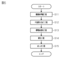
- FIG. 6 is a flow chart illustrating a method for manufacturing an electronic component.
- the electronic component 10 is a multilayer ceramic capacitor.
- the electronic component 10 includes an element body 20.
- the element body 20 is substantially rectangular prism-shaped and has a central axis CA.
- an axis extending along the central axis CA is defined as a first axis X.
- one of the axes perpendicular to the first axis X is defined as a second axis Y.
- an axis perpendicular to the first axis X and the second axis Y is defined as a third axis Z.
- one of the directions along the first axis X is defined as a first positive direction X1, and the direction along the first axis X opposite to the first positive direction X1 is defined as a first negative direction X2.
- one of the directions along the second axis Y is defined as a second positive direction Y1, and the direction along the second axis Y opposite to the second positive direction Y1 is defined as a second negative direction Y2.
- one of the directions along the third axis Z is defined as a third positive direction Z1, and the direction along the third axis Z opposite to the third positive direction Z1 is defined as a third negative direction Z2.
- the outer surface 21 of the element body 20 has six flat surfaces.
- the "surface” of the element body 20 here refers to a surface that can be observed when the entire element body 20 is observed. In other words, even if there are minute irregularities or steps that cannot be seen unless a part of the element body 20 is magnified and observed with a microscope, the surface is expressed as a flat surface or a curved surface.
- the six flat surfaces face in different directions.
- the six flat surfaces are broadly divided into a first end surface 22A facing the first positive direction X1, a second end surface 22B facing the first negative direction X2, and four side surfaces 22C.
- the four side surfaces 22C are a surface facing the third positive direction Z1, a surface facing the third negative direction Z2, a surface facing the second positive direction Y1, and a surface facing the second negative direction Y2, respectively.
- the boundary portions between two adjacent flat surfaces and between three adjacent surfaces of the outer surface 21 of the element body 20 are curved. In other words, the corners of the element body 20 are rounded and chamfered.
- the element body 20 has a dimension along the first axis X that is greater than the dimension along the third axis Z and the dimension along the second axis Y.
- the material of the element body 20 is a dielectric ceramic. Specifically, the material of the element body 20 is mainly composed of BaTiO3 .
- the material of the element body 20 may also be mainly composed of CaTiO3 , SrTiO3 , CaZrO3 , etc.
- the material of the element body 20 may also contain a Mn compound, a Co compound, a Si compound, a rare earth compound, etc. as a secondary component.
- the electronic component 10 has four first internal electrodes 41 and four second internal electrodes 42.
- the first internal electrodes 41 and the second internal electrodes 42 are located inside the element body 20.
- the material of the first internal electrode 41 is a conductive material.
- the material of the first internal electrode 41 is Ni.
- the material of the first internal electrode 41 may further include a metal such as Ni, Cu, Ag, Au, Pt, Sn, Pd, or an alloy containing these metals.
- the material of the second internal electrode 42 is the same as the material of the first internal electrode 41.
- the first internal electrode 41 has a rectangular plate shape.
- the main surface of the first internal electrode 41 is perpendicular to the second axis Y.
- the second internal electrode 42 has the same rectangular plate shape as the first internal electrode 41.
- the main surface of the second internal electrode 42 is perpendicular to the second axis Y, similar to the first internal electrode 41.
- the dimension of the first internal electrode 41 in the direction along the first axis X is smaller than the dimension of the element body 20 in the direction along the first axis X. Also, as shown in FIG. 1, the dimension of the first internal electrode 41 in the direction along the third axis Z is approximately two-thirds of the dimension of the element body 20 in the direction along the third axis Z. The dimensions of the second internal electrode 42 in each direction are the same as those of the first internal electrode 41.
- the first internal electrodes 41 and the second internal electrodes 42 are positioned alternately in the direction along the second axis Y. That is, a total of eight internal electrodes are arranged alternately in the order of the first internal electrodes 41 and the second internal electrodes 42 from the side surface 22C facing the second positive direction Y1 toward the second negative direction Y2. In this embodiment, the distance between each internal electrode in the direction along the second axis Y is equal.
- the four first internal electrodes 41 and the four second internal electrodes 42 are all located at the center of the element body 20 in the direction along the third axis Z.
- the first internal electrodes 41 are located closer to the first positive direction X1.
- the second internal electrodes 42 are located closer to the first negative direction X2.
- the end of the first internal electrode 41 on the first positive direction X1 side is approximately aligned with the end of the element body 20 on the first positive direction X1 side. Therefore, the end of the first internal electrode 41 on the first positive direction X1 side is exposed from the first end surface 22A of the element body 20.
- the end of the first internal electrode 41 on the first negative direction X2 side is located inside the element body 20 and does not reach the end of the element body 20 on the first negative direction X2 side.
- the end of the second internal electrode 42 on the first negative direction X2 side is approximately aligned with the end of the element body 20 on the first negative direction X2 side.
- the end of the second internal electrode 42 on the first negative direction X2 side is exposed from the second end surface 22B of the element body 20.
- the end of the second internal electrode 42 on the first positive direction X1 side is located inside the element body 20 and does not reach the end of the element body 20 on the first positive direction X1 side.
- the electronic component 10 has a first external electrode 61 and a second external electrode 62.
- the first external electrode 61 and the second external electrode 62 are conductive as a whole.
- the first external electrode 61 and the second external electrode 62 do not contain silver components.
- does not contain silver components means that a small amount of silver components is allowed to be mixed into each external electrode during the manufacturing process. For example, if the atomic percentage of silver atoms relative to all atoms constituting each external electrode is less than 1 atm%, it is considered that "the external electrode does not contain silver components.” This is because if the atomic percentage of silver atoms is less than 1 atm%, no significant migration that would affect the characteristics of the electronic component 10 occurs.
- the first external electrode 61 has a first electrode 61A, a second electrode 61B, and a third electrode 61C.
- the first electrode 61A covers a portion of the outer surface 21 of the element body 20. Specifically, the first electrode 61A covers the first end face 22A of the element body 20 and portions of the four side faces 22C in the first positive direction X1.
- the first electrode 61A is connected to the first internal electrode 41 exposed from the first end face 22A.
- the first electrode 61A contains a copper component and a trace amount of glass.
- the second electrode 61B covers the outer surface BD61A of the first electrode 61A. In other words, the second electrode 61B is laminated on the first electrode 61A. Details of the second electrode 61B will be described later.
- the third electrode 61C covers the outer surface BD61B of the second electrode 61B. A portion of the third electrode 61C protrudes from the second electrode 61B. Although not shown, the third electrode 61C has a two-layer structure consisting of a nickel layer and a tin layer, in that order from the second electrode 61B side.
- the second external electrode 62 has a first electrode 62A, a second electrode 62B, and a third electrode 62C.
- the first electrode 62A covers a portion of the outer surface 21 of the element body 20. Specifically, the first electrode 62A covers the second end face 22B of the element body 20 and portions of the four side faces 22C facing the first negative direction X2.
- the first electrode 62A is also connected to the second internal electrode 42 exposed from the second end face 22B.
- the material of the first electrode 62A is the same as the material of the first electrode 61A in the first external electrode 61.
- the second electrode 62B covers the outer surface BD62A of the first electrode 62A. Details of the second electrode 62B will be described later.
- the third electrode 62C covers the outer surface BD62B of the second electrode 62B. A portion of the third electrode 62C protrudes from the second electrode 62B.
- the third electrode 62C has a two-layer structure consisting of a nickel layer and a tin layer, in that order from the second electrode 62B side.
- the second external electrode 62 does not reach the first external electrode 61 on the side surface 22C, and is disposed away from the first external electrode 61 in the direction along the first axis X. Furthermore, the first external electrode 61 and the second external electrode 62 are not stacked in the central portion in the direction along the first axis X on the side surface 22C of the element body 20. Note that in Figures 1 to 3, the first external electrode 61 and the second external electrode 62 are shown by two-dot chain lines.
- the configuration of the second electrode 61B will be described. Note that, although the second electrode 61B of the first external electrode 61 will be described below as a representative, the second electrode 62B of the second external electrode 62 is similarly configured.
- the second electrode 61B is a sintered body containing copper. Specifically, the second electrode 61B contains copper particles 63. Note that in FIG. 5, only some of the copper particles 63 are labeled with reference numerals. Also, although each copper particle 63 is illustrated as being approximately circular, it may be an elliptical or other irregularly shaped particle.
- the second electrode 61B contains, in addition to the copper particles 63, a silicone resin 64 as a synthetic resin.
- the silicone resin 64 contains Si.
- the silicone resin 64 is a polymer consisting of a siloxane bond and a Si-C bond.
- the silicone resin 64 is distributed in a mesh-like pattern. Specifically, when the second electrode 61B is viewed in cross section, the silicone resin 64 is distributed in a mesh-like pattern so as to fill the spaces between the multiple copper particles 63.
- the average value of the thickness H of the second electrode 61B is about 700 nm.
- the thickness H of the second electrode 61B is the shortest distance from the outer surface BD61A of the first electrode 61A to the outer surface BD61B of the second electrode 61B.
- FIG. 4 illustrates the thickness H at one arbitrary point.
- the average value of the thickness H of the second electrode 61B is calculated as follows. First, an arbitrary cross section of the second electrode 61B is photographed with an electron microscope. Next, a range in the direction along the outer surface BD61B of the second electrode 61B is identified for the photographed image.
- the cross-sectional area of the second electrode 61B is calculated by image processing for a measurement range of at least 5 ⁇ m or more. Then, the average value of the thickness H of the second electrode 61B is calculated by dividing the cross-sectional area of the second electrode 61B in the calculated measurement range by the length of the measurement range.
- the second electrode 61B contains a chemical component that is not contained in the second electrode 61B and is contained only in the first electrode 61A.
- the chemical component is a glass component that is a constituent of the first electrode 61A.
- the glass component is spread throughout substantially the entire second electrode 61B.
- the second electrode 61B contains a chemical component that is not contained in the second electrode 61B and is contained only in the third electrode 61C.
- the chemical component is a nickel component that is a constituent component of the third electrode 61C. Note that the nickel component may reach the first electrode 61A.
- the electronic component 10 is viewed in a specific cross section including the first electrode 61A and the second electrode 61B.
- the specific cross section is, for example, a cross section perpendicular to the central axis CA of the element body 20.
- the copper particles 63 of the second electrode 61B are in line contact with the outer surface BD61A of the first electrode 61A.
- the copper particles 63 and the copper component of the first electrode 61A may be integrated, and there may be no boundary between the two copper components.
- the straight line connecting the ends of the contact points with the copper particles 63 is taken as the outer surface BD61A of the first electrode 61A.
- the copper particle 63 which is in line contact with the outer surface BD61A of the first electrode 61A, has a spherical portion BP and a columnar portion PP.
- the columnar portion PP extends from the point of the spherical portion BP facing the first electrode 61A toward the first electrode 61A. This is because part of the copper particle 63 melts during the manufacturing process and becomes integrated with the outer surface BD61A of the first electrode 61A.
- the columnar portion PP may be substantially rectangular, substantially trapezoidal in shape with a width that increases as it approaches the outer surface BD61A, or substantially trapezoidal in shape with a width that decreases as it approaches the outer surface BD61A.
- the maximum width of the columnar portion PP is smaller than the particle diameter of the spherical portion BP.
- the contact length L of the copper particles 63 that are in line contact with the first electrode 61A is 5 nm or more.
- the contact length L is measured as follows. First, in a specific cross section, the outlines of the copper particles 63 and the outer surface BD61A of the first electrode 61A are obtained by image processing using an electron microscope. Then, the number of copper particles 63 that are in contact with the outer surface BD61A within a continuous range of 50 nm or more on the outer surface BD61A is counted. In addition, the total value of the contact lengths L of the copper particles 63 that are in contact with the outer surface BD61A within the same range is measured.
- This total value is divided by the number of copper particles 63 counted to determine the contact length L of each copper particle 63 with the first electrode 61A. It is preferable to measure the contact length L of the copper particles 63 at multiple cross sections, for example, at least two cross sections, for one electronic component 10, and to use the average of the measured values as the final contact length L of the copper particles 63.
- the average particle size of the copper particles 63 is 50 nm or more and 100 nm or less.
- the average particle size of the copper particles 63 is determined as follows. First, the outline of the copper particles 63 is obtained by image processing using an electron microscope. Then, the area of one copper particle 63 is calculated. Then, a circle having the calculated area is assumed. The diameter of the circle is calculated as the particle size of the copper particle 63. In this manner, the particle sizes of 10 or more copper particles 63 are calculated, and the average value is set as the average particle size.
- the contact length L of the copper particles 63 with the outer surface BD61A of the first electrode 61A is 10 nm or more. In this embodiment, the contact length L of the copper particles 63 with the first electrode 61A is 10% or more of the average particle size of the copper particles 63.
- a laminate is prepared.
- the laminate at this stage is in a state before R-chamfering, and is a rectangular parallelepiped with six flat surfaces.
- a plurality of ceramic sheets that will become the element body 20 are prepared.
- the sheets are thin plates.
- a conductive paste that will become the first internal electrode 41 is laminated on the sheets.
- a ceramic sheet that will become the element body 20 is laminated on the paste.
- a conductive paste that will become the second internal electrode 42 is laminated on the sheets. In this way, the ceramic sheets and the conductive paste are laminated alternately.
- the laminated sheets are compressed in the stacking direction by a means such as a mold press.
- the compressed sheet is then cut to a predetermined size to form an unfired laminate.
- the unfired laminate is then fired at a high temperature to prepare the laminate.
- the R-chamfering process S12 is performed.
- the laminate prepared in the laminate preparation process S11 is R-chamfered. This process produces the base body 20 with R-chamfered corners.
- a first conductor paste is applied by a dip method to a portion of the first end face 22A of the element body 20 and a portion of the second end face 22B of the element body 20. Specifically, the first conductor paste is applied so as to cover the entire first end face 22A and portions of the four side faces 22C. The first conductor paste is also applied so as to cover the entire second end face 22B and portions of the four side faces 22C.
- the first conductor paste contains a copper component and a silicon component.
- a second conductor paste is applied onto the first conductor paste at two locations.
- the second conductor paste is a complex ink.
- the second conductor paste is created as follows. First, an amine compound such as 2-ethylhexylamine is mixed with an alcohol amine such as 2-amino-2-methylpropanol. Then, a silicon component such as silicone resin is added at 0.001-10 wt% relative to the weight of Cu alone. Then, a metal salt is further added and dissolved to create the second conductor paste.
- the sintering start temperature of the copper component is 170 degrees
- the hardening start temperature of the silicon component is 250 degrees.
- the hardening step S14 is performed. Specifically, in the hardening step S14, the base body 20 to which the first conductive paste and the second conductive paste are applied is heated. In this embodiment, the base body 20 to which the first conductive paste and the second conductive paste are applied is heated in a nitrogen atmosphere. Then, the temperature is maintained within a range of 300 degrees to 600 degrees. This causes the first conductive paste and the second conductive paste to be fired. During the firing of the second conductive paste, sintering of the copper component contained in the second electrode 61B and the second electrode 62B is first started. At the time when sintering of the copper component starts, the silicon component is not hardened and has fluidity. Therefore, the silicon component fills the gaps between the copper components.
- the hardening start temperature of the silicon component is higher than the sintering start temperature of the copper component.
- the copper component is sintered to produce copper particles 63.
- the silicon component is hardened to produce silicone resin 64.
- the hardening start temperature of the silicon component is higher than the sintering start temperature of the copper component, so the silicone resin 64 becomes a mesh-like structure that fills the gaps between the copper particles 63.
- the second electrode 61B and the second electrode 62B are formed as described above.
- the copper component contained in the second conductive paste is in a state of high surface free energy. Therefore, the copper component contained in the second conductive paste is adsorbed to the copper component contained in the first conductive paste so as to reduce the surface area. As a result, at a specific cross section, the copper particles 63 are in line contact with the first electrode 61A.
- the plating process S15 is performed. Electroplating is performed on the locations where the second electrodes 61B and 62B are located. As a result, the third electrode 61C is formed on the surface of the second electrode 61B. Also, the third electrode 62C is formed on the surface of the second electrode 62B. Although not shown in the figure, the third electrodes 61C and 62C are electroplated with two types of metal, nickel and tin, to form a two-layer structure. In this manner, the electronic component 10 is formed.
- the first external electrode 61 does not contain a silver component, migration in the first external electrode 61 can be suppressed. Furthermore, since the second electrode 61B contains copper particles 63, some of the copper particles 63 fall off when an external force acts on the second electrode 61B. Therefore, the possibility that the entire second electrode 61B will peel off from the first electrode 61A is low. Furthermore, if there is a possibility that all of the copper particles 63 fall off when an external force acts on the second electrode 61B, there is a risk that electrical connection cannot be made between the second electrode 61B and the first electrode 61A.
- the copper particles 63 are in line contact with the outer surface BD61A of the first electrode 61A, good conductivity can be ensured between the first electrode 61A and the second electrode 61B.
- the contact length L of the copper particles 63 that are in line contact with the first electrode 61A in the specific cross section is 5 nm or more. Because the copper particles 63 are in line contact with the first electrode 61A with the above dimensions, the second electrode 61B is less likely to peel off from the first electrode 61A.
- the contact length L of the copper particles 63 that are in line contact with the first electrode 61A in a specific cross section is 10% or more of the average particle size of the copper particles 63.
- the second electrode 61B contains silicone resin 64 as the synthetic resin. That is, the synthetic resin contained in the second electrode 61B contains Si. By containing Si in the synthetic resin, the surface tension of the synthetic resin is easily maintained between the copper particles 63 during manufacturing. As a result, in the formed second electrode 61B, the synthetic resin becomes a dense film that fills the gaps between the copper particles 63. As a result, the barrier properties of the second electrode 61B are improved.
- the second electrode 61B contains a chemical component that is not contained in the second electrode 61B and is contained only in the first electrode 61A. With this configuration, at least a portion of the second electrode 61B is integrated with the first electrode 61A. As a result, the second electrode 61B is less likely to peel off from the first electrode 61A.
- the second electrode 61B contains a chemical component that is not contained in the second electrode 61B and is contained only in the third electrode 61C. With this configuration, at least a portion of the second electrode 61B is integrated with the third electrode 61C. As a result, the third electrode 61C is not easily peeled off from the second electrode 61B.
- the first electrode 61A contains a copper component.
- the copper particles 63 contained in the second electrode 61B are easily integrated with the copper components contained in the first electrode 61A during the manufacturing process. Therefore, since many copper particles 63 are in line contact with the first electrode 61A, it is expected that the adhesion strength of the second electrode 61B to the first electrode 61A will be improved.
- the electronic component 10 is not limited to a multilayer ceramic capacitor.
- the electronic component 10 may be a piezoelectric component, a thermistor, an inductor, or the like.
- the material of the element body 20 may be a dielectric material, a piezoelectric material, a magnetic material such as ferrite, or a composite material of synthetic resin and metal.
- the shape of the element body 20 is not limited to the example of the above embodiment.
- the element body 20 may be a polygonal column shape other than a rectangular column shape having a central axis CA.
- the element body 20 may also be the core of a wire-wound inductor component.
- the core may have a so-called drum core shape.
- the core may have a cylindrical winding core portion and flange portions provided at each end of the winding core portion.
- the boundary portion between adjacent flat surfaces of the outer surface 21 of the element body 20 does not have to be chamfered. In this case, no curved surface exists at the boundary portion.
- the first internal electrodes 41 and the second internal electrodes 42 may have any shape as long as they can ensure electrical conduction with the corresponding first external electrodes 61 and second external electrodes 62. In addition, the number of first internal electrodes 41 and second internal electrodes 42 does not matter and may be less than four or more than four.
- the material of the first electrode 61A is not limited to the example of the above embodiment. In other words, the first electrode 61A does not have to contain a copper component.
- the material of the first electrode 61A may be a metal such as Ni, Pd, or Au, or may be a composition containing any of these metals.
- the second electrode 61B may cover at least a portion of the first electrode 61A.
- the average value of the thickness H of the second electrode 61B is not limited to the example of the above embodiment.
- the overall thickness of the first external electrode 61 including the second electrode 61B may be designed taking into consideration the mechanical strength required of the electronic component 10, etc.
- the configuration related to the third electrode 61C in the first external electrode 61 may be omitted.
- the material of the third electrode 61C is not limited to the example in the above embodiment.
- the third electrode 61C may be made of only nickel, may be made of only tin, or may contain materials other than silver.
- the synthetic resin is not limited to silicone resin 64.
- the synthetic resin may be a synthetic resin containing Si, such as silicone oligomer.
- the synthetic resin contained in the second electrode 61B may also contain N.
- the synthetic resin may be a synthetic resin containing N, such as urethane, epoxy, polyimide, polyimide amide, or polyamide. In this way, when the synthetic resin contains N, the heat resistance of the second electrode 61B is improved.
- the synthetic resin is not limited to resins containing N and Si, but may be resins such as acrylic, alkyd, polyester, or other synthetic resins.
- the second electrode 61B may use as its synthetic resin a composite of these synthetic resins containing N, synthetic resins containing Si, and other synthetic resins.
- the second electrode 61B may use as its synthetic resin a synthetic resin that contains Si and N in one type of synthetic resin.
- the contact length L of the copper particles 63 in linear contact with the first electrode 61A is not limited to the example of the above embodiment.
- the contact length L of the copper particles 63 in linear contact with the first electrode 61A may be less than 5 nm as long as electrical conduction with the first electrode 61A is ensured.
- the contact length L of the copper particles 63 in linear contact with the first electrode 61A may be less than 10% of the average particle size of the copper particles 63.
- the average particle size of the copper particles 63 is also not limited to the example of the above embodiment.
- the second electrode 61B may not contain a chemical component that is not included in the second electrode 61B and is contained only in the first electrode 61A. That is, the boundary between the second electrode 61B and the first electrode 61A may be clearly separated.
- the second electrode 61B may not contain a chemical component that is not included in the second electrode 61B and is contained only in the third electrode 61C. That is, the boundary between the second electrode 61B and the third electrode 61C may be clearly separated.
- the manufacturing process of the electronic component 10 in the above embodiment is not limited to the example in the above embodiment.
- the element body 20 may be subjected to a process such as physical polishing.
- the method for applying the first conductive paste and the second conductive paste is not limited to the example in the above embodiment.
- these pastes may be applied by printing, or may be applied by an inkjet method or the like.
- the first conductive paste and the second conductive paste may be applied by different methods.
- the curing step S14 may be performed in a plurality of steps. That is, the baking may be performed in a plurality of steps.
- the sintering start temperature of the copper component and the hardening start temperature of the silicon component of the second conductive paste are not limited to the examples in the above embodiment.
- the second conductive paste may be a nano-ink. If it is a nano-ink, it is created as follows. Nano-metal powder is dispersed in a solvent containing cellosolves, carbitols, hydrocarbons, aromatics, etc. Then, various silicone-modified resins, silicone resins, sol-gel-based materials, etc. are added in an amount of 0.001-10 wt % relative to the weight of Cu alone. The second conductive paste of nano-ink may be created in this way, or a different method may be used.
- the material when the second conductive paste is a complex ink is not limited to the example of the above embodiment.
- the amine compound may be any of primary amines, secondary amines, and tertiary amines, and the number of N atoms is not limited.
- it may be a primary amine such as octylamine or hexylamine, a secondary amine such as di-n-butylamine, or a tertiary amine such as N,N-dimethylhexylamine.
- the amine compound may also be an alcohol amine or diamine, and the positional relationship between the N atom and the OH group is not specified as ⁇ , ⁇ , ⁇ , etc.
- the number of N and O atoms in one molecule is not particularly limited.
- it may be an ⁇ -hydroxyamine such as 2-dimethylaminoethanol or 2-ethylaminoethanol, or a ⁇ -hydroxyamine such as 3-amino-1-propanol or 4-amino-2-butanol.
- it may be a diamine such as ethylenediamine, or a cyclic diamine such as piperazine.
- the silicon component may be, for example, various silicone-modified resins such as epoxy resins, polyester resins, and phenolic resins, and sol-gel materials.
- Metal salts made of formic acid, acetic acid, oxalic acid, and other organic acids may also be used.
- An example of this type of metal salt is anhydrous copper formate.
- the electronic component 10 may be provided with a glass film.
- the glass film may be formed so as to cover a partial area of the outer surface 21 of the element body 20. In other words, even if there is a glass film covering the element body 20, it is sufficient that the electrical connection between the first internal electrode 41 and the first external electrode 61, and the electrical connection between the second internal electrode 42 and the second external electrode 62 are ensured.
- An electronic component comprising: an element body; an internal electrode located inside the element body; and an external electrode covering a portion of the outer surface of the element body and not containing a silver component, wherein the external electrode has a first electrode covering a portion of the outer surface of the element body and connected to the internal electrode, and a second electrode covering the outer surface of the first electrode, wherein the second electrode contains copper particles and a synthetic resin, and when viewed in cross section at a specific cross section including the first electrode and the second electrode, the copper particles of the second electrode are in line contact with the outer surface of the first electrode.
- the external electrode further includes a third electrode covering the outer surface of the second electrode, the second electrode containing a chemical component that is not included in the second electrode and is contained only in the first electrode, and the second electrode containing a chemical component that is not included in the second electrode and is contained only in the third electrode.
- Reference Signs List 10 Electronic component 20: Body 21: Outer surface 41: First internal electrode 42: Second internal electrode 61: First external electrode 61A: First electrode 61B: Second electrode 61C: Third electrode 63: Copper particles 64: Silicone resin
Landscapes
- Engineering & Computer Science (AREA)
- Power Engineering (AREA)
- Manufacturing & Machinery (AREA)
- Microelectronics & Electronic Packaging (AREA)
- Chemical & Material Sciences (AREA)
- Ceramic Engineering (AREA)
- Inorganic Chemistry (AREA)
- Fixed Capacitors And Capacitor Manufacturing Machines (AREA)
Priority Applications (2)
| Application Number | Priority Date | Filing Date | Title |
|---|---|---|---|
| JP2024529435A JPWO2024257381A1 (https=) | 2023-06-14 | 2024-01-11 | |
| US19/017,840 US20250149248A1 (en) | 2023-06-14 | 2025-01-13 | Electronic component that suppresses migration in external electodes |
Applications Claiming Priority (2)
| Application Number | Priority Date | Filing Date | Title |
|---|---|---|---|
| JP2023-098070 | 2023-06-14 | ||
| JP2023098070 | 2023-06-14 |
Related Child Applications (1)
| Application Number | Title | Priority Date | Filing Date |
|---|---|---|---|
| US19/017,840 Continuation US20250149248A1 (en) | 2023-06-14 | 2025-01-13 | Electronic component that suppresses migration in external electodes |
Publications (1)
| Publication Number | Publication Date |
|---|---|
| WO2024257381A1 true WO2024257381A1 (ja) | 2024-12-19 |
Family
ID=93851615
Family Applications (1)
| Application Number | Title | Priority Date | Filing Date |
|---|---|---|---|
| PCT/JP2024/000441 Ceased WO2024257381A1 (ja) | 2023-06-14 | 2024-01-11 | 電子部品 |
Country Status (3)
| Country | Link |
|---|---|
| US (1) | US20250149248A1 (https=) |
| JP (1) | JPWO2024257381A1 (https=) |
| WO (1) | WO2024257381A1 (https=) |
Citations (3)
| Publication number | Priority date | Publication date | Assignee | Title |
|---|---|---|---|---|
| JP2013235807A (ja) * | 2012-05-04 | 2013-11-21 | Samsung Electro-Mechanics Co Ltd | 導電性樹脂組成物、これを含む積層セラミックキャパシタ及びその製造方法 |
| JP2014160791A (ja) * | 2013-02-20 | 2014-09-04 | Samsung Electro-Mechanics Co Ltd | 積層セラミック電子部品 |
| JP2022067931A (ja) * | 2020-10-21 | 2022-05-09 | Tdk株式会社 | 電子部品 |
Family Cites Families (1)
| Publication number | Priority date | Publication date | Assignee | Title |
|---|---|---|---|---|
| KR20160125121A (ko) * | 2015-04-21 | 2016-10-31 | 삼성전기주식회사 | 적층 세라믹 커패시터 및 그 제조 방법 |
-
2024
- 2024-01-11 JP JP2024529435A patent/JPWO2024257381A1/ja active Pending
- 2024-01-11 WO PCT/JP2024/000441 patent/WO2024257381A1/ja not_active Ceased
-
2025
- 2025-01-13 US US19/017,840 patent/US20250149248A1/en active Pending
Patent Citations (3)
| Publication number | Priority date | Publication date | Assignee | Title |
|---|---|---|---|---|
| JP2013235807A (ja) * | 2012-05-04 | 2013-11-21 | Samsung Electro-Mechanics Co Ltd | 導電性樹脂組成物、これを含む積層セラミックキャパシタ及びその製造方法 |
| JP2014160791A (ja) * | 2013-02-20 | 2014-09-04 | Samsung Electro-Mechanics Co Ltd | 積層セラミック電子部品 |
| JP2022067931A (ja) * | 2020-10-21 | 2022-05-09 | Tdk株式会社 | 電子部品 |
Also Published As
| Publication number | Publication date |
|---|---|
| US20250149248A1 (en) | 2025-05-08 |
| JPWO2024257381A1 (https=) | 2024-12-19 |
Similar Documents
| Publication | Publication Date | Title |
|---|---|---|
| US10840021B2 (en) | Multilayer ceramic electronic component | |
| CN111952076B (zh) | 电子部件的安装构造体及其制造方法 | |
| JP5870895B2 (ja) | セラミック電子部品及びその製造方法 | |
| US10453612B2 (en) | Multilayer ceramic capacitor | |
| JP7522585B2 (ja) | 電子部品、回路基板および電子部品の製造方法 | |
| JP2015109410A (ja) | セラミック電子部品及びセラミック電子部品の製造方法 | |
| CN103377823B (zh) | 多层陶瓷电子元件及其制造方法 | |
| KR20140030611A (ko) | 외부 전극용 도전성 페이스트 조성물, 이를 포함하는 적층 세라믹 전자 부품 및 그 제조 방법 | |
| JP2022142213A (ja) | セラミック電子部品、実装基板およびセラミック電子部品の製造方法 | |
| JP2021034440A (ja) | 積層セラミック電子部品 | |
| CN115881434B (zh) | 层叠陶瓷电容器 | |
| JP2013118357A (ja) | セラミック電子部品及びその製造方法 | |
| US12567541B2 (en) | Electronic component and method for manufacturing electronic component | |
| WO2023095620A1 (ja) | 積層セラミック電子部品 | |
| JP2004296936A (ja) | セラミック電子部品 | |
| WO2024257381A1 (ja) | 電子部品 | |
| CN114678215A (zh) | 多层电子组件 | |
| JP7715289B2 (ja) | 電子部品 | |
| WO2024166504A1 (ja) | 電子部品及び電子部品の実装構造 | |
| CN115223791B (zh) | 陶瓷电子元件和基板装置 | |
| JP7491246B2 (ja) | 導電性ペーストおよびセラミック電子部品 | |
| JP3807609B2 (ja) | セラミック電子部品及びその製造方法 | |
| CN120359585A (zh) | 层叠陶瓷电子部件 | |
| WO2024166447A1 (ja) | 電子部品 | |
| WO2025220548A1 (ja) | 電子部品 |
Legal Events
| Date | Code | Title | Description |
|---|---|---|---|
| WWE | Wipo information: entry into national phase |
Ref document number: 2024529435 Country of ref document: JP |
|
| 121 | Ep: the epo has been informed by wipo that ep was designated in this application |
Ref document number: 24823005 Country of ref document: EP Kind code of ref document: A1 |
|
| NENP | Non-entry into the national phase |
Ref country code: DE |