WO2024252555A1 - ウエハ載置台 - Google Patents
ウエハ載置台 Download PDFInfo
- Publication number
- WO2024252555A1 WO2024252555A1 PCT/JP2023/021151 JP2023021151W WO2024252555A1 WO 2024252555 A1 WO2024252555 A1 WO 2024252555A1 JP 2023021151 W JP2023021151 W JP 2023021151W WO 2024252555 A1 WO2024252555 A1 WO 2024252555A1
- Authority
- WO
- WIPO (PCT)
- Prior art keywords
- flow path
- wafer mounting
- mounting surface
- branch
- wafer
- Prior art date
- Legal status (The legal status is an assumption and is not a legal conclusion. Google has not performed a legal analysis and makes no representation as to the accuracy of the status listed.)
- Ceased
Links
Images




Classifications
-
- H—ELECTRICITY
- H10—SEMICONDUCTOR DEVICES; ELECTRIC SOLID-STATE DEVICES NOT OTHERWISE PROVIDED FOR
- H10P—GENERIC PROCESSES OR APPARATUS FOR THE MANUFACTURE OR TREATMENT OF DEVICES COVERED BY CLASS H10
- H10P72/00—Handling or holding of wafers, substrates or devices during manufacture or treatment thereof
- H10P72/70—Handling or holding of wafers, substrates or devices during manufacture or treatment thereof for supporting or gripping
- H10P72/76—Handling or holding of wafers, substrates or devices during manufacture or treatment thereof for supporting or gripping using mechanical means, e.g. clamps or pinches
- H10P72/7604—Handling or holding of wafers, substrates or devices during manufacture or treatment thereof for supporting or gripping using mechanical means, e.g. clamps or pinches the wafers being placed on a susceptor, stage or support
- H10P72/7624—Handling or holding of wafers, substrates or devices during manufacture or treatment thereof for supporting or gripping using mechanical means, e.g. clamps or pinches the wafers being placed on a susceptor, stage or support characterised by the mechanical construction of the susceptor, stage or support
-
- H—ELECTRICITY
- H10—SEMICONDUCTOR DEVICES; ELECTRIC SOLID-STATE DEVICES NOT OTHERWISE PROVIDED FOR
- H10P—GENERIC PROCESSES OR APPARATUS FOR THE MANUFACTURE OR TREATMENT OF DEVICES COVERED BY CLASS H10
- H10P72/00—Handling or holding of wafers, substrates or devices during manufacture or treatment thereof
- H10P72/70—Handling or holding of wafers, substrates or devices during manufacture or treatment thereof for supporting or gripping
- H10P72/72—Handling or holding of wafers, substrates or devices during manufacture or treatment thereof for supporting or gripping using electrostatic chucks
- H10P72/722—Details of electrostatic chucks
-
- C—CHEMISTRY; METALLURGY
- C23—COATING METALLIC MATERIAL; COATING MATERIAL WITH METALLIC MATERIAL; CHEMICAL SURFACE TREATMENT; DIFFUSION TREATMENT OF METALLIC MATERIAL; COATING BY VACUUM EVAPORATION, BY SPUTTERING, BY ION IMPLANTATION OR BY CHEMICAL VAPOUR DEPOSITION, IN GENERAL; INHIBITING CORROSION OF METALLIC MATERIAL OR INCRUSTATION IN GENERAL
- C23C—COATING METALLIC MATERIAL; COATING MATERIAL WITH METALLIC MATERIAL; SURFACE TREATMENT OF METALLIC MATERIAL BY DIFFUSION INTO THE SURFACE, BY CHEMICAL CONVERSION OR SUBSTITUTION; COATING BY VACUUM EVAPORATION, BY SPUTTERING, BY ION IMPLANTATION OR BY CHEMICAL VAPOUR DEPOSITION, IN GENERAL
- C23C16/00—Chemical coating by decomposition of gaseous compounds, without leaving reaction products of surface material in the coating, i.e. chemical vapour deposition [CVD] processes
- C23C16/44—Chemical coating by decomposition of gaseous compounds, without leaving reaction products of surface material in the coating, i.e. chemical vapour deposition [CVD] processes characterised by the method of coating
- C23C16/458—Chemical coating by decomposition of gaseous compounds, without leaving reaction products of surface material in the coating, i.e. chemical vapour deposition [CVD] processes characterised by the method of coating characterised by the method used for supporting substrates in the reaction chamber
- C23C16/4582—Rigid and flat substrates, e.g. plates or discs
- C23C16/4583—Rigid and flat substrates, e.g. plates or discs the substrate being supported substantially horizontally
- C23C16/4585—Devices at or outside the perimeter of the substrate support, e.g. clamping rings, shrouds
-
- C—CHEMISTRY; METALLURGY
- C23—COATING METALLIC MATERIAL; COATING MATERIAL WITH METALLIC MATERIAL; CHEMICAL SURFACE TREATMENT; DIFFUSION TREATMENT OF METALLIC MATERIAL; COATING BY VACUUM EVAPORATION, BY SPUTTERING, BY ION IMPLANTATION OR BY CHEMICAL VAPOUR DEPOSITION, IN GENERAL; INHIBITING CORROSION OF METALLIC MATERIAL OR INCRUSTATION IN GENERAL
- C23C—COATING METALLIC MATERIAL; COATING MATERIAL WITH METALLIC MATERIAL; SURFACE TREATMENT OF METALLIC MATERIAL BY DIFFUSION INTO THE SURFACE, BY CHEMICAL CONVERSION OR SUBSTITUTION; COATING BY VACUUM EVAPORATION, BY SPUTTERING, BY ION IMPLANTATION OR BY CHEMICAL VAPOUR DEPOSITION, IN GENERAL
- C23C16/00—Chemical coating by decomposition of gaseous compounds, without leaving reaction products of surface material in the coating, i.e. chemical vapour deposition [CVD] processes
- C23C16/44—Chemical coating by decomposition of gaseous compounds, without leaving reaction products of surface material in the coating, i.e. chemical vapour deposition [CVD] processes characterised by the method of coating
- C23C16/458—Chemical coating by decomposition of gaseous compounds, without leaving reaction products of surface material in the coating, i.e. chemical vapour deposition [CVD] processes characterised by the method of coating characterised by the method used for supporting substrates in the reaction chamber
- C23C16/4582—Rigid and flat substrates, e.g. plates or discs
- C23C16/4583—Rigid and flat substrates, e.g. plates or discs the substrate being supported substantially horizontally
- C23C16/4586—Elements in the interior of the support, e.g. electrodes, heating or cooling devices
-
- H—ELECTRICITY
- H01—ELECTRIC ELEMENTS
- H01J—ELECTRIC DISCHARGE TUBES OR DISCHARGE LAMPS
- H01J37/00—Discharge tubes with provision for introducing objects or material to be exposed to the discharge, e.g. for the purpose of examination or processing thereof
- H01J37/32—Gas-filled discharge tubes
- H01J37/32431—Constructional details of the reactor
- H01J37/32623—Mechanical discharge control means
- H01J37/32642—Focus rings
-
- H—ELECTRICITY
- H01—ELECTRIC ELEMENTS
- H01J—ELECTRIC DISCHARGE TUBES OR DISCHARGE LAMPS
- H01J37/00—Discharge tubes with provision for introducing objects or material to be exposed to the discharge, e.g. for the purpose of examination or processing thereof
- H01J37/32—Gas-filled discharge tubes
- H01J37/32431—Constructional details of the reactor
- H01J37/32715—Workpiece holder
- H01J37/32724—Temperature
-
- H—ELECTRICITY
- H10—SEMICONDUCTOR DEVICES; ELECTRIC SOLID-STATE DEVICES NOT OTHERWISE PROVIDED FOR
- H10P—GENERIC PROCESSES OR APPARATUS FOR THE MANUFACTURE OR TREATMENT OF DEVICES COVERED BY CLASS H10
- H10P72/00—Handling or holding of wafers, substrates or devices during manufacture or treatment thereof
- H10P72/04—Apparatus for manufacture or treatment
- H10P72/0431—Apparatus for thermal treatment
- H10P72/0434—Apparatus for thermal treatment mainly by convection
-
- H—ELECTRICITY
- H10—SEMICONDUCTOR DEVICES; ELECTRIC SOLID-STATE DEVICES NOT OTHERWISE PROVIDED FOR
- H10P—GENERIC PROCESSES OR APPARATUS FOR THE MANUFACTURE OR TREATMENT OF DEVICES COVERED BY CLASS H10
- H10P72/00—Handling or holding of wafers, substrates or devices during manufacture or treatment thereof
- H10P72/70—Handling or holding of wafers, substrates or devices during manufacture or treatment thereof for supporting or gripping
- H10P72/72—Handling or holding of wafers, substrates or devices during manufacture or treatment thereof for supporting or gripping using electrostatic chucks
-
- H—ELECTRICITY
- H10—SEMICONDUCTOR DEVICES; ELECTRIC SOLID-STATE DEVICES NOT OTHERWISE PROVIDED FOR
- H10P—GENERIC PROCESSES OR APPARATUS FOR THE MANUFACTURE OR TREATMENT OF DEVICES COVERED BY CLASS H10
- H10P72/00—Handling or holding of wafers, substrates or devices during manufacture or treatment thereof
- H10P72/70—Handling or holding of wafers, substrates or devices during manufacture or treatment thereof for supporting or gripping
- H10P72/76—Handling or holding of wafers, substrates or devices during manufacture or treatment thereof for supporting or gripping using mechanical means, e.g. clamps or pinches
- H10P72/7604—Handling or holding of wafers, substrates or devices during manufacture or treatment thereof for supporting or gripping using mechanical means, e.g. clamps or pinches the wafers being placed on a susceptor, stage or support
- H10P72/7611—Handling or holding of wafers, substrates or devices during manufacture or treatment thereof for supporting or gripping using mechanical means, e.g. clamps or pinches the wafers being placed on a susceptor, stage or support characterised by edge profile or support profile
Definitions
- the present invention relates to a wafer mounting table.
- a wafer mounting table that includes a ceramic plate having a wafer mounting surface on the upper surface, a cooling plate provided on the lower surface of the ceramic plate, and a refrigerant flow path built into the cooling plate.
- Patent Document 1 discloses a wafer mounting table in which the cooling plate is formed of a material with high thermal conductivity such as Al, in which the distance between the upper surface of the refrigerant flow path and the wafer mounting surface is constant from the inlet to the outlet of the refrigerant flow path, and the cross-sectional shape of the refrigerant flow path varies depending on the position of the refrigerant flow path.
- Patent Document 1 describes that the cross-sectional area of the flow path corresponding to the relatively high temperature part of the wafer mounting surface is smaller than the cross-sectional area of the flow path corresponding to the relatively low temperature part of the wafer mounting surface. It also describes that the width of the upper surface of the refrigerant flow path from the inlet to the outlet of the refrigerant flow path is constant, and the height direction length of the refrigerant flow path is shorter at the position corresponding to the relatively high temperature part of the wafer mounting surface than at the position corresponding to the relatively low temperature part of the wafer mounting surface.
- Patent Document 1 suppresses uneven heat transfer in the refrigerant flow path by devising a cross-sectional shape for the cooling plate, for example, when the width through which the refrigerant flow path can pass is narrow, it is not possible to ensure a sufficient cross-sectional area of the flow path corresponding to the relatively low temperature area of the wafer placement surface, and thus it is not possible to sufficiently suppress uneven heat transfer.
- the present invention was made to solve these problems, and its main purpose is to suppress temperature unevenness on the wafer mounting surface of a wafer mounting table.
- the wafer mounting table of the present invention comprises: a ceramic plate having a wafer mounting surface on an upper surface thereof; a cooling plate provided on a lower surface of the ceramic plate; A refrigerant flow path built into the cooling plate; A wafer mounting table comprising: The coolant flow path has a first portion and a second portion that branches into two or more branches from the first portion and runs parallel to each other, a cross-sectional area of the first portion is smaller than the sum of the cross-sectional areas of each branch of the second portion; It is something.
- the refrigerant flow path has a first portion and a second portion that branches off from the first portion into two or more branches that run parallel to each other. Therefore, even when the width through which the refrigerant flow path can pass is narrow, each branch of the second portion can be made to fit within that width while ensuring a relatively large flow path cross-sectional area for the entire second portion.
- the cross-sectional area of the first portion is smaller than the sum of the cross-sectional areas of the branches of the second portion. Therefore, the first portion of the refrigerant flow path has a faster flow rate than the second portion, resulting in higher cooling efficiency. Therefore, by adjusting the arrangement of the first and second portions of the wafer mounting table, such as by arranging the first portion to correspond to an area with high cooling demands, it is possible to suppress temperature unevenness on the wafer mounting surface.
- the first portion may be arranged corresponding to the outer circumferential region of the wafer mounting surface, and the second portion may be arranged corresponding to the central region of the wafer mounting surface.
- the heat input of plasma into the wafer mounting table is greater in the outer circumferential region of the wafer mounting surface than in the central region.
- the ceramic plate may have an annular focus ring mounting surface around the wafer mounting surface that is one step lower than the height of the wafer mounting surface, and an annular focus ring having an outer diameter larger than the outer diameter of the ceramic plate and the outer diameter of the cooling plate may be mounted on the focus ring mounting surface.
- the focus ring protrudes outside the wafer mounting table (overhangs), the peripheral region of the wafer mounting surface is likely to become hotter. Therefore, there is great significance in applying the present invention.
- the cross-sectional area of each branch of the second portion may be greater than half the cross-sectional area of the first portion. The larger the cross-sectional area of each branch of the second portion, the slower the flow rate of each branch, and therefore the relatively faster flow rate of the first portion, thereby further suppressing uneven heat transfer.
- the refrigerant flow path may have a turn-back section that reverses the direction of the flow path and branches into two in the middle of the turn-back section to suppress bias in the amount of refrigerant distributed to each branch in the second section. In this way, bias in the heat removal capacity of each branch is suppressed, and uneven heat removal can be further suppressed.
- the refrigerant flow path may be branched into a branch that continues the tendency of curvature before the branching and a branch that deviates from the tendency of curvature to the outside, thereby suppressing bias in the amount of refrigerant distributed to each branch of the second portion. This also suppresses bias in the heat removal capacity of each branch, and further suppresses uneven heat removal.
- the non-flow path area which is the area of the portion in which the refrigerant flow path is not formed, may be 50% or more.
- the larger the non-flow path area the greater the degree of freedom in arranging the configuration other than the refrigerant flow path.
- the wafer mounting surface may have an area with a high cooling requirement and an area with a low cooling requirement, and the first portion may be disposed in the area of the wafer mounting surface corresponding to the area with a high cooling requirement, and the second portion may be disposed in the area of the wafer mounting surface with a low cooling requirement.
- the area with a high cooling requirement may be the peripheral area of the wafer mounting surface
- the area with a low cooling requirement may be the central area of the wafer mounting surface.
- the heat exchange efficiency of the region of the wafer mounting surface that corresponds to the first portion may be higher than the heat exchange efficiency of the region that corresponds to the second portion.
- the region of the wafer mounting surface that corresponds to the first portion may be a peripheral region of the wafer mounting surface
- the region of the wafer mounting surface that corresponds to the second portion may be a central region of the wafer mounting surface.
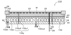
- FIG. FIG. 2 is a cross-sectional view taken along line AA in FIG. 1 .
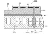
- FIG. 2 is a partially enlarged view of FIG.
- FIG. 4 is an explanatory diagram of the results of a study on the flow of a refrigerant in a refrigerant flow path.
- FIG. FIG. BB cross-sectional view of FIG. 6.
- FIG. 7 is a partially enlarged view of FIG. 6 .
- Fig. 1 is a cross-sectional view of a wafer mounting table 10 (a cross-sectional view when the wafer mounting table 10 is cut on a plane including the central axis of the wafer mounting table 10)
- Fig. 2 is a plan view of the wafer mounting table 10
- Fig. 3 is a cross-sectional view taken along the line A-A in Fig. 1
- Fig. 4 is a partially enlarged view of Fig. 1
- Fig. 5 is an explanatory diagram of the results of examining the flow of a refrigerant in a refrigerant flow path.
- Fig. 1 is a cross-sectional view of a wafer mounting table 10 (a cross-sectional view when the wafer mounting table 10 is cut on a plane including the central axis of the wafer mounting table 10)
- Fig. 2 is a plan view of the wafer mounting table 10
- Fig. 3 is a cross-sectional view taken along the line A-A in Fig. 1
- FIG. 5A is a vector diagram showing the flow velocity distribution in the refrigerant flow path (the original diagram is a color diagram in which red, orange, yellow, green, blue, indigo, and purple are used in order of increasing flow velocity), and Figs. 5B and 5C are explanatory diagrams showing preferred branching forms.
- the wafer mounting table 10 is used to perform CVD, etching, etc. on the wafer W using plasma.
- the wafer mounting table 10 includes a ceramic plate 20, a cooling plate 30, and a bonding layer 40.
- the ceramic plate 20 is made of a ceramic material such as alumina or aluminum nitride.
- the ceramic plate 20 has a wafer mounting surface 22, an electrostatic electrode 23, and a focus ring mounting surface 24.
- the focus ring may be abbreviated as "FR.”
- the wafer mounting surface 22 is a circular surface provided on the upper surface of the ceramic plate 20.
- the wafer W is placed on the wafer mounting surface 22.
- the wafer mounting surface 22 has a plurality of gas holes 50 (six in this embodiment) that penetrate the wafer mounting table 10 in the vertical direction, and a thermally conductive gas such as He gas is supplied from a gas supply source (not shown).
- a thermally conductive gas such as He gas is supplied from a gas supply source (not shown).
- the wafer mounting surface 22 has an annular seal band formed along the outer edge, and a plurality of small circular protrusions are formed on the entire surface of the area surrounded by the seal band.
- the seal band and the small circular protrusions are the same height, and the height is, for example, several ⁇ m to several tens of ⁇ m.
- the wafer mounting surface 22 has areas that are prone to high temperatures (areas with high cooling requirements) and areas that are not prone to high temperatures (areas with low cooling requirements).
- the heat input of the plasma is greater on the outer periphery side, so as shown in FIG. 2, the outer periphery region 22a (lightly shaded region) of the wafer mounting surface 22 is an area requiring high cooling, and the central region 22b (darkly shaded region) of the wafer mounting surface 22 is an area requiring low cooling.
- the electrostatic electrode 23 is a planar mesh electrode or plate electrode, and is connected to a DC power source (not shown) via a power supply terminal 26.
- a DC voltage is applied to the electrostatic electrode 23
- the wafer W is attracted and fixed to the wafer mounting surface 22 (specifically, the upper surface of the seal band and the upper surfaces of the small circular protrusions) by electrostatic attraction, and when the application of the DC voltage is released, the wafer W is released from the attraction and fixation to the wafer mounting surface 22.
- the power supply terminal 26 is inserted into a terminal hole 56 provided in the wafer mounting table 10 between the lower surface of the electrostatic electrode 23 and the lower surface of the cooling plate 30.
- the FR mounting surface 24 is provided in an annular shape around the wafer mounting surface 22.
- the height of the FR mounting surface 24 is one step lower than the height of the wafer mounting surface 22.
- An annular focus ring 60 is mounted on the FR mounting surface 24.
- the focus ring 60 is made of, for example, Si.
- a circumferential groove 62 is provided on the upper part of the inner surface of the focus ring 60 so that it does not come into contact with the wafer W.
- the outer diameter of the focus ring 60 is larger than the outer diameter of the ceramic plate 20 and the outer diameter of the cooling plate 30. Therefore, the focus ring 60 is placed on the FR mounting surface 24 in a state where it protrudes outside the wafer mounting table 10 (overhanging state).
- the cooling plate 30 is a disk-shaped plate having a refrigerant flow path 32 through which a refrigerant can circulate. As shown in FIG. 3, the refrigerant flow path 32 is provided so as to cover the entire surface of the ceramic plate 20 from one end (inlet 32in) to the other end (outlet 32out) in a plan view. In this embodiment, the refrigerant flow path 32 is formed in a spiral shape in a plan view.
- Such a cooling plate 30 can be manufactured, for example, by diffusion bonding a plurality of layered members.
- the refrigerant is supplied to the inlet 32in of the refrigerant flow path 32 from a refrigerant circulation device (not shown), passes through the refrigerant flow path 32, and is discharged from the outlet 32out of the refrigerant flow path 32 and returns to the refrigerant circulation device.
- the refrigerant circulation device can adjust the refrigerant to a desired temperature.
- the refrigerant is preferably a liquid, and is preferably electrically insulating.
- An example of an electrically insulating liquid is a fluorine-based inert liquid.
- Examples of materials used for the cooling plate 30 include metal materials and composite materials of metal and ceramic.
- Examples of metal materials include Al, Ti, Mo, and alloys thereof.
- Examples of composite materials of metal and ceramic include metal matrix composites (MMC) and ceramic matrix composites (CMC). Specific examples of such composite materials include materials containing Si, SiC, and Ti (also called SiSiCTi), materials in which a SiC porous body is impregnated with Al and/or Si, and composite materials of Al 2 O 3 and TiC. From the viewpoint of suppressing warping of the wafer mounting table 10, it is preferable that the material used for the cooling plate 30 has a thermal expansion coefficient close to that of the ceramic plate 20.
- the material of the cooling plate 30 is pure Ti or an ⁇ - ⁇ Ti alloy. This is because the thermal expansion coefficients of pure Ti and ⁇ - ⁇ Ti alloys are close to that of alumina.
- the material used for the cooling plate 30 is preferably one having a high thermal conductivity, for example, Al.
- the thermal conductivity of Al is 150 to 200 W/mK.
- the cooling plate 30 may be formed of a material having a lower thermal conductivity than Al.
- such a material may be a Ti-containing material.
- the thermal conductivity of the cooling plate 30 may be 50 W/mK or less, or may be 5 to 20 W/mK.
- the thermal conductivity of pure Ti is 17 W/mK
- the thermal conductivity of an ⁇ - ⁇ Ti alloy is 7.5 W/mK.
- the material used for the cooling plate 30 may be a conductive material.
- the bonding layer 40 bonds the lower surface of the ceramic plate 20 to the upper surface of the cooling plate 30.
- the bonding layer 40 may be, for example, a metal layer formed from solder or a metal brazing material, or a resin layer formed from a resin adhesive.
- the refrigerant flow path 32 has a first portion 32x corresponding to the outer peripheral region 22a (region with high cooling demand) of the wafer mounting surface 22, and a second portion 32y corresponding to the central region 22b (region with low cooling demand).
- the first portion 32x corresponding to the outer peripheral region 22a of the refrigerant flow path 32 is the portion from the inlet 32in to the midway position 32mid of the refrigerant flow path 32.
- the second portion 32y corresponding to the central region 22b of the refrigerant flow path 32 is the portion from the midway position 32mid to the outlet 32out of the refrigerant flow path 32.
- the second portion 32y branches into two branches, 32y1 and 32y2, at the branch point 32div at the midway position 32mid, and joins at the joining point 32join to reach the outlet 32out.
- the branch point 32div is located at the midway position 32mid, but the branch point 32div may be located at a position away from the midway position 32mid.
- the refrigerant flow path 32 has a turn section 32turn that reverses the direction of the flow path, and branches into two branches, 32y1 and 32y2, at a branch point 32div located midway through the turn section 32turn.
- the turn section 32turn reverses the counterclockwise direction from the inlet 32in to the turn section 32turn to a clockwise direction from the turn section 32turn to the outlet 32out.
- the refrigerant flow path 32 is formed to branch into two branches, 32y1 and 32y2, at a branch point 32div located midway through the turn section 32turn, thereby preventing the amount of refrigerant distributed to each branch 32y1, 32y2 from being biased toward one of the branches (this point will be described later using Figure 5).
- the flow path cross-sectional area Sx of the first part 32x corresponding to the outer peripheral region 22a is smaller than the sum of the flow path cross-sectional areas Sy1, Sy2 of the branches 32y1, 32y2 of the second part 32y corresponding to the central region 22b, that is, Sx ⁇ Sy1+Sy2.
- the smaller the flow path cross-sectional area S the faster the flow rate of the refrigerant flowing through the refrigerant flow path 32, and the higher the cooling efficiency.
- the flow path cross-sectional area S is the area of the cross section (flow path cross section) when the refrigerant flow path 32 is cut on a plane perpendicular to the longitudinal direction of the refrigerant flow path 32 (each branch 32y1, 32y2 in the second part 32y).
- the flow path cross-sectional area S of the refrigerant flow path 32 is the horizontal length W multiplied by the vertical length H.
- the horizontal length W and the vertical length H may be set appropriately according to the flow path cross-sectional area S.
- the wafer mounting table 10 is fixed inside a semiconductor process chamber (not shown).
- a focus ring 60 is placed on the FR mounting surface 24, and a wafer W is placed on the wafer mounting surface 22.
- a DC voltage is applied to the electrostatic electrode 23 to adsorb the wafer W to the wafer mounting surface 22.
- a thermally conductive gas (such as He gas) is supplied to a gas hole 50 (a passage from the lower surface of the cooling plate 30 to the wafer mounting surface 22) provided inside the wafer mounting table 10.
- the gas fills the space surrounded by the lower surface of the wafer W and the seal band of the wafer mounting surface 22, improving the thermal conduction between the wafer W and the wafer mounting surface 22.
- the interior of the chamber is then set to a predetermined vacuum atmosphere (or reduced pressure atmosphere), and an RF voltage is applied to the cooling plate 30 while supplying a process gas from a shower head provided on the ceiling of the chamber. Then, a plasma is generated between the wafer W and the shower head. The plasma is then used to perform CVD film formation and etching on the wafer W.
- the heat input from the plasma is greater in the outer peripheral region of the wafer W than in the central region, and therefore the outer peripheral region of the wafer W is more likely to become hotter than the central region. Therefore, to make the temperature of the wafer W uniform, it is necessary to cool the outer peripheral region 22a of the wafer mounting surface 22 more efficiently than the central region 22b.
- the cross-sectional area S of the coolant flow path 32 is adjusted as described above. As a result, the first portion 32x of the coolant flow path 32 corresponding to the outer peripheral region 22a has a higher cooling efficiency than the second portion 32y corresponding to the central region 22b.
- the refrigerant flow path 32 has a first portion 32x corresponding to an area with high cooling demand and a second portion 32y corresponding to an area with low cooling demand.
- the second portion 32y branches into two branches 32y1 and 32y2 at a branch point 32div from the first portion 32x, and the branches run parallel to each other. Therefore, even if the width through which the refrigerant flow path 32 can pass is narrow, for example, because the distance between the gas hole 50 and the terminal hole 56 is close, the second portion 32y as a whole can secure a relatively large flow path cross-sectional area while making each branch 32y1 and 32y2 of the second portion fit within that width.
- the flow path cross-sectional area Sx of the first portion 32x corresponding to the area with high cooling demand of the refrigerant flow path 32 is smaller than the sum Sy1+Sy2 of the flow path cross-sectional areas of each branch 32y1 and 32y2 of the second portion 32y corresponding to the area with low cooling demand. Therefore, the first portion 32x of the refrigerant flow path 32 corresponding to the region with high cooling demand has a faster flow rate than the second portion 32y corresponding to the region with low cooling demand, and the cooling efficiency is improved.
- the first portion 32x corresponding to the region with high cooling demand has one branch
- the second portion 32y corresponding to the region with low cooling demand has two or more branches to control the flow rate
- the flow rate can be controlled by changing the flow path cross-sectional area of the first portion 32x and the second portion 32y. Therefore, by adjusting the arrangement of the first portion 32x and the second portion 32y, such as by arranging the first portion 32x so as to correspond to the region with high cooling demand, the temperature unevenness of the wafer mounting surface 22 can be suppressed, and the temperature uniformity of the wafer W can be improved.
- the flow path cross-sectional area S of the refrigerant flow path 32 may satisfy 1.5Sx ⁇ Sy1+Sy2 ⁇ 2.5Sx, or 1.8Sx ⁇ Sy1+Sy2 ⁇ 2.2Sx.
- the plasma heat input to the wafer mounting table 10 is generally greater in the outer peripheral region 22a of the wafer mounting surface 22 than in the central region 22b.
- the first portion 32x is disposed at a position corresponding to the outer peripheral region 22a of the wafer mounting surface 22, and the second portion 32y is disposed at a position corresponding to the central region 22b of the wafer mounting surface 22, thereby making it possible to make the cooling efficiency of the outer peripheral region 22a of the wafer mounting surface 22 higher than that of the central region 22b, and thus effectively suppressing temperature unevenness in the wafer mounting surface 22.
- the ceramic plate 20 has an annular focus ring mounting surface 24 around the wafer mounting surface 22, which is one step lower than the height of the wafer mounting surface 22, and an annular focus ring 60 having an outer diameter larger than the outer diameter of the ceramic plate 20 and the outer diameter of the cooling plate 30 is mounted on the focus ring mounting surface 24.
- the focus ring 60 protrudes outside the wafer mounting table 10 (overhangs), the peripheral region 22a of the wafer mounting surface 22 is likely to become hotter. Therefore, there is great significance in applying the present invention.
- the flow path cross-sectional areas Sy1, Sy2 of each branch 32y1, 32y2 of the second portion 32y are both greater than 1/2 the flow path cross-sectional area Sx of the first portion 32x.
- the larger the flow path cross-sectional areas Sy1, Sy2 of each branch 32y1, 32y2 of the second portion 32y the slower the flow rate of each branch 32y1, 32y2, and the more the heat dissipation unevenness can be suppressed.
- the flow path cross-sectional areas Sy1, Sy2 of each branch 32y1, 32y2 may be 2/3 or more, or 3/4 or more, of the flow path cross-sectional area Sx of the first portion 32x.
- the flow path cross-sectional areas Sy1, Sy2 of each branch 32y1, 32y2 may be 2 times or less, or 1.5 times or less, of the flow path cross-sectional area Sx of the first portion 32x.
- the refrigerant flow path 32 has a turn section 32turn that reverses the direction of the flow path, and branches into two branches 32y1 and 32y2 at a branch point 32div midway through the turn section 32turn, suppressing bias in the amount of refrigerant distributed to each branch 32y1 and 32y2 of the second part 32y. This suppresses bias in the heat removal capacity of each branch 32y1 and 32y2, and further suppresses uneven heat removal.
- a turn-back part with a smaller curvature for example, a curvature radius R of 20 mm or less
- the previous curved shape for example, a curvature radius R of 50 mm or more
- the centrifugal force is canceled once in the middle of the turn-back, and the flow rate becomes the highest near the center of the flow path, as in part (2) of FIG. 5A, and the difference in flow rate between the outer periphery side (outside the curve) and the inner periphery side (inside the curve) becomes small. Therefore, for example, if the flow path is branched into two at a branch point in the middle of the turn-back part, as in FIG.
- the amount of refrigerant distributed to each branch is prevented from being biased toward one of the branches. If the branch point is located midway through the turnaround section, it is preferable to place the branch point near the center of the flow path where the flow velocity is greater near the center than on either side.
- a non-flow passage area which is an area of a portion where the refrigerant flow passage 32 is not formed, may be 50% or more in a region where the second portion 32y is arranged (e.g., the central region 22b where cooling requirements are low).
- the non-flow path area when the temperature unevenness of the wafer is within a predetermined range was 41.3% in the former case, while it was 54.6% in the latter case, and the non-flow path area could be increased to 50% or more.
- Sx flow path cross-sectional area
- Sy 168 mm2
- a length Wy 14 mm
- a length Hy 12 mm.
- the non-flow path area may be, for example, 70% or less.
- the region in which the second portion 32y is arranged (here, the central region 22b) may be the minimum circumscribed circle that includes all of the branches 32y1 and 32y2.
- the ratio Ly1/Ly2 of the lengths Ly1, Ly2 (not shown) of the branches 32y1, 32y2 is 4/5 or more and 5/4 or less. In this way, the pressure loss difference between the branches 32y1 and 32y2 can be reduced. Note that, when the ratio Ly1/Ly2 is large, the pressure loss difference between the branches 32y1 and 32y2 can be reduced by adjusting the cross-sectional shape of each branch 32y1, 32y2.
- the lengths Ly1, Ly2 of each branch 32y1, 32y2 may be 1/2 or more of the length Lx of the first portion 32x, or may be greater than or equal to the length Lx of the first portion 32x.
- the lengths Ly1, Ly2 of each branch 32y1, 32y2 may be 10 times or less, or 5 times or less, of the length Lx of the first portion 32x.
- the length Lx of the first portion 32x and the lengths Ly1 and Ly2 of the branches 32y1 and 32y2 may each be 20 mm or more.
- the ratio Sy1/Sy2 of the flow path cross-sectional areas Sy1 and Sy2 of the branches 32y1 and 32y2 is 4/5 or more and 5/4 or less. In this way, the pressure loss difference between the branches 32y1 and 32y2 can be reduced.
- Fig. 6 is a cross-sectional view of the wafer mounting table 110 (a cross-sectional view when the wafer mounting table 110 is cut along a plane including the central axis of the wafer mounting table 110),
- Fig. 7 is a plan view of the wafer mounting table 110,
- Fig. 8 is a cross-sectional view taken along the line B-B of Fig. 6, and
- Fig. 9 is a partially enlarged view of Fig. 6.
- the same components as those in the above-mentioned embodiment are designated by the same reference numerals, and their description will be omitted.
- the refrigerant flow path 132 is provided so as to cover the entire surface of the ceramic plate 20 from one end (inlet 132in) to the other end (outlet 132out) in a plan view.
- the refrigerant flow path 132 is formed in a spiral shape.
- the refrigerant and the refrigerant circulation device can be the same as those in the above-mentioned embodiment.
- the refrigerant flow path 132 has a first portion 132x corresponding to the outer peripheral region 22a (region with high cooling demand) of the wafer placement surface 22, and a second portion 132y corresponding to the central region 22b (region with low cooling demand).
- the first portion 132x corresponding to the outer peripheral region 22a of the refrigerant flow path 132 is the portion from the inlet 132in to the midpoint 132mid of the refrigerant flow path 132.
- the second portion 132y corresponding to the central region 22b of the refrigerant flow path 132 is the portion from the midpoint 132mid to the outlet 132out of the refrigerant flow path 132.
- the second portion 132y branches into two branches, 132y1 and 132y2, at the branch point 132div, joins at the joining point 132join, and reaches the outlet 132out.
- the refrigerant flow path 132 is formed so that it branches at the branch point 132div into a branch 132y1 that continues the curved tendency before the branch, and a branch 132y2 that deviates from this curved tendency to the outside, thereby preventing the amount of refrigerant distributed to each branch 132y1, 132y2 from being biased toward one of the branches.
- the flow path cross-sectional area Sx of the first portion 132x corresponding to the outer peripheral region 22a is smaller than the sum of the flow path cross-sectional areas Sy1, Sy2 of the branches 132y1, 132y2 of the second portion 132y corresponding to the central region 22b, i.e., Sx ⁇ Sy1+Sy2. Therefore, the first portion 132x corresponding to the region of the refrigerant flow path 132 with high cooling demand has a faster flow rate and higher cooling efficiency than the second portion 132y corresponding to the region with low cooling demand.
- the flow path cross-sectional area S, horizontal length W, and vertical length H of the refrigerant flow path 132 are equivalent to the flow path cross-sectional area S, horizontal length W, and vertical length H of the refrigerant flow path 32.
- the use examples of the wafer mounting table 110 are similar to the manufacturing and use examples of the wafer mounting table 10, so their explanation will be omitted here.
- the first portion 132x corresponding to the area with high cooling demand has one branch
- the second portion 132y corresponding to the area with low cooling demand has two or more branches to control the flow rate. Furthermore, by controlling the flow rate by changing the flow path cross-sectional area between the first portion 132x and the second portion 132y, the wafer mounting table 110 can suppress temperature unevenness on the wafer mounting surface 22, thereby improving the thermal uniformity of the wafer W.
- the refrigerant flow path 132 is formed to branch at the branch point 132div into a branch 132y1 that continues the curved tendency before the branch, and a branch 132y2 that deviates from this curved tendency to the outside, thereby preventing the amount of refrigerant distributed to each branch 132y1, 132y2 from being biased toward one branch. This prevents bias in the heat removal capacity of each branch 132y1, 132y2, and further prevents uneven heat removal.
- the branch 132y2 may branch at an angle of 30° to 90° with respect to the branch 132y1.
- the branch on the inner periphery becomes the mainstream flow path, suppressing the amount of refrigerant distributed to the branch on the outer periphery (outside the curve), and suppressing the amount of refrigerant distributed to each branch from being biased toward one branch.
- the non-flow path area which is the area of the portion where the refrigerant flow path 132 is not formed, may be 50% or more.
- the larger the non-flow path area the greater the degree of freedom in arranging the components other than the refrigerant flow path (gas holes 50, terminal holes 56, lift pin holes described below, etc.).
- the non-flow path area may be, for example, 70% or less.
- the length L and cross-sectional area S of the refrigerant flow path 132 may be made equivalent to the length L and cross-sectional area S of the refrigerant flow path 32, thereby reducing the pressure loss difference between the branches 132y1 and 132y2.
- the refrigerant flow paths 32, 132 are branched into two paths, but they may be branched into three or more paths.
- the arrangement of the branching points 32div, 132div of the refrigerant flow paths 32, 132 is not limited to that described above, and may be appropriately set so that the amount of refrigerant distributed to each branch 32y1, 32y2 and each branch 132y1, 132y2 is the desired amount.
- the refrigerant flow paths 32, 132 are assumed to merge at the junctions 32join, 132join, but they may also lead to outlets provided individually in each branch 32y1, 32y2 or each branch 132y1, 132y2 without merging.
- the area with high cooling demand is the peripheral area 22a of the wafer mounting surface 22, and the area with low cooling demand is the central area 22b of the wafer mounting surface 22, but this is not particularly limited.
- the heat exchange efficiency of the peripheral region 22a of the wafer mounting surface 22 corresponding to the first portion 32x, 132x may be higher than the heat exchange efficiency of the central region 22b corresponding to the second portion 32y, 132y.
- the heat exchange efficiency can be obtained as follows, taking the wafer mounting table 10 as an example. First, a first chiller capable of circulating a refrigerant while controlling the temperature of the refrigerant is connected to the inlet 32in and outlet 32out of the refrigerant flow path 32, and a refrigerant at the same temperature as room temperature (e.g., 25°C) is circulated through the refrigerant flow path 32.
- a refrigerant at a predetermined temperature (e.g., 80 to 100°C) is prepared in the second chiller. Then, the refrigerant at the same temperature as room temperature is switched to a refrigerant at the predetermined temperature by a valve, and the refrigerant at the predetermined temperature is circulated through the refrigerant flow path 32. After a predetermined time (e.g., 10 seconds) has elapsed since the refrigerant was switched, the temperature distribution of the wafer mounting surface 22 is measured. The temperature rise rate (temperature rise per unit time (°C/sec)) is calculated from the temperature distribution, and the temperature rise rate is used as an index of heat exchange efficiency.
- a predetermined time e.g. 10 seconds
- the temperature rise rate of the outer peripheral region 22a of the wafer mounting surface 22 is 5.5°C/sec or more, and the temperature rise rate of the central region 22b is 5°C/sec or less. Therefore, it can be seen that the heat exchange efficiency of the outer peripheral region 22a is higher than that of the central region 22b.
- the temperature rise rate of the boundary between the outer peripheral region 22a and the central region 22b is an intermediate value.
- the electrostatic electrode 23 is built into the ceramic plate 20 at a position facing the wafer mounting surface 22.
- an FR adsorption electrode for electrostatically adsorbing the focus ring 60 may be provided inside the ceramic plate 20 at a position facing the FR mounting surface 24.
- the ceramic plate 20 is exemplified as having a wafer mounting surface 22 and an FR mounting surface 24, but is not particularly limited to this.
- the ceramic plate 20 may have a wafer mounting surface 22 but not an FR mounting surface 24.
- the outer diameter of the focus ring 60 is illustrated as being larger than the outer diameter of the wafer mounting table 10 (the outer diameter of the ceramic plate 20 and the outer diameter of the cooling plate 30), but is not limited to this.
- the outer diameter of the focus ring 60 may be the same as the outer diameter of the wafer mounting table 10.
- the refrigerant flow paths 32, 132 are formed in a spiral shape when viewed from above, but this is not particularly limited.
- the refrigerant flow paths 32, 132 may be formed in a zigzag shape when viewed from above.
- a wafer mounting table 10 having an electrostatic electrode 23 built into the ceramic plate 20 is exemplified, but this is not particularly limited.
- a heater electrode resistive heating element
- RF electrode plasma generation electrode
- the wafer mounting table 10, 110 may have a plurality of lift pin holes that penetrate the wafer mounting table 10, 110 from top to bottom.
- the lift pin holes are holes for inserting lift pins that move the wafer W up and down relative to the wafer mounting surface 22.
- a plurality of lift pin holes are provided at equal intervals along concentric circles of the wafer mounting surface 22 when the wafer mounting surface 22 is viewed in a plan view.
- the present invention can be used, for example, in an apparatus for plasma processing wafers.
Landscapes
- Chemical & Material Sciences (AREA)
- Engineering & Computer Science (AREA)
- Chemical Kinetics & Catalysis (AREA)
- Plasma & Fusion (AREA)
- Analytical Chemistry (AREA)
- General Chemical & Material Sciences (AREA)
- Physics & Mathematics (AREA)
- Materials Engineering (AREA)
- Mechanical Engineering (AREA)
- Metallurgy (AREA)
- Organic Chemistry (AREA)
- Container, Conveyance, Adherence, Positioning, Of Wafer (AREA)
- Drying Of Semiconductors (AREA)
Abstract
ウエハ載置台10は、上面にウエハ載置面22を有するセラミックプレート20と、セラミックプレート20の下面に設けられた冷却プレートとを備える。冷却プレートに内蔵された冷媒流路32は、第1部分32xと、第1部分32xから2股以上に分岐して分岐同士が並走する第2部分32yと、を有し、前記第1部分32xの断面積は、前記第2部分32yの各分岐の断面積の合計より小さい。
Description
本発明は、ウエハ載置台に関する。
従来、上面にウエハ載置面を有するセラミックプレートと、セラミックプレートの下面に設けられた冷却プレートと、冷却プレートに内蔵された冷媒流路とを備えたウエハ載置台が知られている。例えば、特許文献1には、冷却プレートをAlのような熱伝導率の高い材料で形成したウエハ載置台において、冷媒流路の上面とウエハ載置面との距離が冷媒流路の入口から出口までの間で一定で、冷媒流路の断面形状が冷媒流路の位置に応じて異なるものが開示されている。特許文献1では、ウエハ載置面の温度が相対的に高い部分に対応する流路断面積は、ウエハ載置面の温度が相対的に低い部分に対応する流路断面積よりも小さくする点が記載されている。また、冷媒流路の入口から出口までの間の冷媒流路の上面の幅を一定とし、冷媒流路の高さ方向の長さを、ウエハ載置面の温度が相対的に高い部分に対応する位置の方がウエハ載置面の温度が相対的に低い部分に対応する位置よりも短くする点も記載されている。
しかしながら、特許文献1の構成は、冷却プレートの断面形状を工夫することで冷媒流路の抜熱むらを抑制しているが、例えば、冷媒流路を通すことのできる幅が狭い場合などに、ウエハ載置面の温度が相対的に低い領域に対応する流路断面積を十分に確保できず、抜熱むらを十分に抑制できないことがあった。
本発明はこのような課題を解決するためになされたものであり、ウエハ載置台において、ウエハ載置面の温度むらを抑制することを主目的とする。
[1]本発明のウエハ載置台は、
上面にウエハ載置面を有するセラミックプレートと、
前記セラミックプレートの下面に設けられた冷却プレートと、
前記冷却プレートに内蔵された冷媒流路と、
を備えたウエハ載置台であって、
前記冷媒流路は、第1部分と、前記第1部分から2股以上に分岐して分岐同士が並走する第2部分と、を有し、
前記第1部分の断面積は、前記第2部分の各分岐の断面積の合計よりも小さい、
ものである。
上面にウエハ載置面を有するセラミックプレートと、
前記セラミックプレートの下面に設けられた冷却プレートと、
前記冷却プレートに内蔵された冷媒流路と、
を備えたウエハ載置台であって、
前記冷媒流路は、第1部分と、前記第1部分から2股以上に分岐して分岐同士が並走する第2部分と、を有し、
前記第1部分の断面積は、前記第2部分の各分岐の断面積の合計よりも小さい、
ものである。
このウエハ載置台では、冷媒流路は、第1部分と、第1部分から2股以上に分岐して分岐同士が並走する第2部分と、を有する。そのため、冷媒流路を通すことのできる幅が狭い場合などでも、第2部分の各分岐をその幅に収まるようにしつつ、第2部分全体では比較的大きな流路断面積を確保できる。そして、第1部分の断面積は、第2部分の各分岐の断面積の合計よりも小さい。そのため、冷媒流路のうち第1部分の方が、第2部分よりも流速が速くなり冷却効率が高くなる。したがって、ウエハ載置台において、冷却要求の高い領域に対応するように第1部分を配置するなど、第1部分及び第2部分の配置を調整することにより、ウエハ載置面の温度むらを抑制することができる。
[2]本発明のウエハ載置台(前記[1]に記載のウエハ載置台)において、前記第1部分は、前記ウエハ載置面の外周領域に対応して配置され、前記第2部分は、前記ウエハ載置面の中央領域に対応して配置されていてもよい。一般的に、ウエハ載置台におけるプラズマの入熱は、ウエハ載置面の外周領域の方が中央領域よりも多くなる。この点を考慮して、第1部分及び第2部分を上述のように配置することで、ウエハ載置面の外周領域の冷却効率を中央領域よりも高くすることができ、ひいてはウエハ載置面の温度むらを効果的に抑制することができる。
[3]本発明のウエハ載置台(前記[2]に記載のウエハ載置台)において、前記セラミックプレートは、前記ウエハ載置面の周りに前記ウエハ載置面の高さよりも一段低い環状のフォーカスリング載置面を有していてもよく、前記フォーカスリング載置面には、外径が前記セラミックプレートの外径及び前記冷却プレートの外径よりも大きい環状のフォーカスリングが載置されるものとしてもよい。この場合、フォーカスリングはウエハ載置台の外側にはみ出ているため(オーバーハング)、ウエハ載置面の外周領域がより高温になりやすい。そのため、本発明を適用する意義が高い。
[4]本発明のウエハ載置台(前記[1]~[3]のいずれかに記載のウエハ載置台)において、前記第2部分の各分岐の断面積は、前記第1部分の断面積の1/2より大きいものとしてもよい。第2部分の各分岐の断面積が大きいほど、各分岐の流速が遅くなるため、相対的に第1部分の流速が速くなり、抜熱むらをより抑制できる。
[5]本発明のウエハ載置台(前記[1]~[4]のいずれかに記載のウエハ載置台)において、前記冷媒流路は、流路の向きを反転させる折り返し部を有し、該折り返し部の途中で2股に分岐して、前記第2部分の各分岐に分配される冷媒量の偏りを抑制するものとしてもよい。こうすれば、各分岐の抜熱能力の偏りが抑制され、抜熱むらをより抑制できる。
[6]本発明のウエハ載置台(前記[1]~[4]のいずれかに記載のウエハ載置台)において、前記冷媒流路は、分岐前の湾曲の傾向を引き継ぐ分岐と、前記湾曲の傾向から一旦外側に外れる分岐と、に分岐して、前記第2部分の各分岐に分配される冷媒量の偏りを抑制するものとしてもよい。こうしても、各分岐の抜熱能力の偏りが抑制され、抜熱むらをより抑制できる。
[7]本発明のウエハ載置台(前記[1]~[6]のいずれかに記載のウエハ載置台)において、平面視したときに、前記第2部分が配置された領域において、前記冷媒流路が形成されていない部分の面積である非流路面積が50%以上であるものとしてもよい。非流路面積が大きいほど、冷媒流路以外の構成の配置の自由度を高めることができる。
[8]本発明のウエハ載置台(前記[1]~[7]のいずれかに記載のウエハ載置台)において、前記ウエハ載置面は、冷却要求の高い領域と冷却要求の低い領域とを有し、前記第1部分は前記ウエハ載置面のうち冷却要求の高い領域に対応して配置され、前記第2部分は前記ウエハ載置面のうち冷却要求の低い領域に配置されていてもよい。例えば、冷却要求の高い領域とはウエハ載置面の外周領域であり、冷却要求の低い領域とはウエハ載置面の中央領域であるものとしてもよい。
[9]本発明のウエハ載置台(前記[1]~[8]のいずれかに記載のウエハ載置台)において、前記ウエハ載置面のうち、前記第1部分に対応する領域の熱交換効率は、前記第2部分に対応する領域の熱交換効率よりも高いものとしてもよい。このとき、ウエハ載置面のうち第1部分に対応する領域はウエハ載置面の外周領域であり、ウエハ載置面のうち第2部分に対応する領域はウエハ載置面の中央領域であるものとしてもよい。
[第1実施形態]
本発明の第1実施形態について、図面を用いて説明する。図1はウエハ載置台10の断面図(ウエハ載置台10の中心軸を含む面でウエハ載置台10を切断したときの断面図)、図2はウエハ載置台10の平面図、図3は図1のA-A断面図、図4は図1の部分拡大図、図5は冷媒流路内での冷媒の流れを検討した結果の説明図である。なお、図5Aは、冷媒流路内の流速分布を示すベクトル図(原図は、流速が速い方から赤→橙→黄→緑→青→藍→紫で表されたカラー図面)であり、図5B及び図5Cは、好適な分岐形態を示す説明図である。
本発明の第1実施形態について、図面を用いて説明する。図1はウエハ載置台10の断面図(ウエハ載置台10の中心軸を含む面でウエハ載置台10を切断したときの断面図)、図2はウエハ載置台10の平面図、図3は図1のA-A断面図、図4は図1の部分拡大図、図5は冷媒流路内での冷媒の流れを検討した結果の説明図である。なお、図5Aは、冷媒流路内の流速分布を示すベクトル図(原図は、流速が速い方から赤→橙→黄→緑→青→藍→紫で表されたカラー図面)であり、図5B及び図5Cは、好適な分岐形態を示す説明図である。
ウエハ載置台10は、ウエハWにプラズマを利用してCVDやエッチングなどを行うために用いられるものである。ウエハ載置台10は、セラミックプレート20と、冷却プレート30と、接合層40とを備えている。
セラミックプレート20は、アルミナ、窒化アルミニウムなどに代表されるセラミック材料で形成されている。セラミックプレート20は、ウエハ載置面22と、静電電極23と、フォーカスリング載置面24とを有する。以下、フォーカスリングは「FR」と略すことがある。
ウエハ載置面22は、円形の面であり、セラミックプレート20の上面に設けられている。ウエハ載置面22には、ウエハWが載置される。ウエハ載置面22には、ウエハ載置台10を上下方向に貫通するガス穴50が複数個(本実施形態では6個)開口しており、図示しないガス供給源からHeガスのような熱伝導ガスが供給される。ウエハ載置面22には、図示しないが、外縁に沿って環状のシールバンドが形成され、そのシールバンドに囲まれた領域の全面に複数の円形小突起が形成されている。シールバンド及び円形小突起は同じ高さであり、その高さは例えば数μm~数10μmである。ウエハ載置面22には、高温になりやすい領域(冷却要求の高い領域)と高温になりにくい領域(冷却要求の低い領域)とが存在する。本実施形態では、ウエハWをプラズマで処理する際にプラズマの入熱が外周側で多くなるため、図2に示すように、ウエハ載置面22の外周領域22a(薄い網掛けの領域)が冷却要求の高い領域、ウエハ載置面22の中央領域22b(濃い網掛けの領域)が冷却要求の低い領域になる。
静電電極23は、平面状のメッシュ電極又はプレート電極であり、給電端子26を介して図示しない直流電源に接続される。この静電電極23に直流電圧が印加されるとウエハWは静電吸着力によりウエハ載置面22(具体的にはシールバンドの上面及び円形小突起の上面)に吸着固定され、直流電圧の印加を解除するとウエハWのウエハ載置面22への吸着固定が解除される。給電端子26は、ウエハ載置台10のうち静電電極23の下面と冷却プレート30の下面との間に設けられた端子穴56に挿通される。
FR載置面24は、ウエハ載置面22の周りに環状に設けられている。FR載置面24の高さは、ウエハ載置面22の高さよりも一段低くなっている。FR載置面24には、環状のフォーカスリング60が載置される。フォーカスリング60は、例えばSiで形成されている。フォーカスリング60の内側面の上方には、ウエハWと接触しないように円周溝62が設けられている。フォーカスリング60の外径は、セラミックプレート20の外径や冷却プレート30の外径よりも大きい。そのため、フォーカスリング60は、ウエハ載置台10の外側にはみ出した状態(オーバーハングした状態)でFR載置面24に載置される。
冷却プレート30は、内部に冷媒が循環可能な冷媒流路32を備えた、円盤状のプレートである。冷媒流路32は、図3に示すように、平面視で一端(入口32in)から他端(出口32out)までセラミックプレート20の全面にわたるように設けられている。冷媒流路32は、本実施形態では平面視で渦巻き状に形成されている。こうした冷却プレート30は、例えば複数の層状部材を拡散接合することにより作製することができる。冷媒は、図示しない冷媒循環装置から冷媒流路32の入口32inに供給され、冷媒流路32を通過したあと冷媒流路32の出口32outから排出されて冷媒循環装置に戻る。冷媒循環装置は冷媒を所望の温度に調節することができる。冷媒は、液体が好ましく、電気絶縁性であることが好ましい。電気絶縁性の液体としては、例えばフッ素系不活性液体などが挙げられる。
冷却プレート30に用いる材料としては、金属材料や金属とセラミックとの複合材料などが挙げられる。金属材料としては、Al、Ti、Mo又はそれらの合金などが挙げられる。金属とセラミックとの複合材料としては、金属マトリックス複合材料(MMC)やセラミックマトリックス複合材料(CMC)などが挙げられる。こうした複合材料の具体例としては、Si、SiC及びTiを含む材料(SiSiCTiともいう)、SiC多孔質体にAl及び/又はSiを含浸させた材料、Al2O3とTiCとの複合材料などが挙げられる。冷却プレート30に用いる材料としては、ウエハ載置台10が反るのを抑制する観点からは、熱膨張係数がセラミックプレート20に近いものが好ましい。セラミックプレート20の材料がアルミナの場合、冷却プレート30の材料は純Tiかα-βTi合金であることが好ましい。純Tiやα-βTi合金の熱膨張係数は、アルミナの熱膨張係数に近いからである。冷却プレート30に用いる材料としては、抜熱性能を高める観点からは、熱伝導率の高いものが好ましく、例えばAlであることが好ましい。Alの熱伝導率は150~200W/mKである。冷却プレート30は、Alよりも熱伝導率の低い材料で形成されていてもよい。こうした材料としては、例えば、Ti含有材料などが挙げられる。冷却プレート30の熱伝導率は、50W/mK以下であるものとしてもよく、5~20W/mKであるものとしてもよい。例えば、純Tiの熱伝導率は17W/mK、α-βTi合金の熱伝導率は7.5W/mKである。また、冷却プレート30に用いる材料は、導電材料としてもよい。
接合層40は、セラミックプレート20の下面と冷却プレート30の上面とを接合する。接合層40は、例えば、はんだや金属ロウ材で形成された金属層であってもよいし、樹脂接着剤で形成された樹脂層であってもよい。
冷媒流路32について詳しく説明する。冷媒流路32には、図2に示すように、ウエハ載置面22の外周領域22a(冷却要求の高い領域)に対応する第1部分32xと、中央領域22b(冷却要求の低い領域)に対応する第2部分32yとが存在する。冷媒流路32のうち外周領域22aに対応する第1部分32xは、冷媒流路32の入口32inから途中位置32midまでの部分である。冷媒流路32のうち中央領域22bに対応する第2部分32yは、冷媒流路32の途中位置32midから出口32outまでの部分である。第2部分32yは、途中位置32midにある分岐点32divで分岐32y1と分岐32y2との2股に分岐し、合流点32joinで合流して、出口32outにいたる。なお、図2,3では、途中位置32midに分岐点32divが配置されているが、途中位置32midから離れた位置に分岐点32divが配置されていてもよい。
冷媒流路32は、流路の向きを反転させる折り返し部32turnを有し、折り返し部32turnの途中にある分岐点32divで分岐32y1と分岐32y2との2股に分岐する。折り返し部32turnは、入口32inから折り返し部32turnまでの反時計回りを、折り返し部32turnから出口32outまでの時計回りに反転させる。冷媒流路32は、折り返し部32turnの途中にある分岐点32divで分岐32y1と分岐32y2との2股に分岐するように形成されており、これにより、各分岐32y1,32y2に分配される冷媒量が一方の分岐に偏るのを抑制する(この点は図5を用いて後述する)。
冷媒流路32の流路断面積Sについては、図4に示すように外周領域22aに対応する第1部分32xの流路断面積Sxの方が、中央領域22bに対応する第2部分32yの各分岐32y1,32y2の流路断面積Sy1,Sy2の合計よりも小さい、つまりSx<Sy1+Sy2である。流路断面積Sが小さいほど、冷媒流路32を流れる冷媒の流速が速くなり冷却効率が高くなる。なお、流路断面積Sは、冷媒流路32(第2部分32yにおいては各分岐32y1,32y2)の長手方向と垂直な面で冷媒流路32を切断したときの断面(流路断面)の面積である。第2部分32yの各分岐32y1,32y2の流路断面積Sy1,Sy2は、適宜設定すればよいが、本実施形態では、第1部分32xの流路断面積Sxと同じ、つまりSy1=Sy2=Sxである。冷媒流路32の流路断面積Sは、横の長さWに縦の長さHを乗じた値である。横の長さW及び縦の長さHは、流路断面積Sに応じて適宜設定すればよい。本実施形態では、第2部分32yの各分岐32y1,32y2の横の長さWy1,Wy2は、第1部分32xの横の長さWxと同じ、つまりWy1=Wy2=Wxである。また、第2部分32yの各分岐32y1,32y2の縦の長さHy1,Hy2は、第1部分32xの縦の長さHxと同じ、つまりHy1=Hy2=Hxである。
次に、ウエハ載置台10の使用例について説明する。図示しない半導体プロセス用のチャンバの内部に、ウエハ載置台10を固定する。FR載置面24には、フォーカスリング60が載置され、ウエハ載置面22には、ウエハWが載置される。この状態で、静電電極23に直流電圧を印加してウエハWをウエハ載置面22に吸着させる。それと共に、ウエハ載置台10の内部に設けられたガス穴50(冷却プレート30の下面からウエハ載置面22に至る通路)に、熱伝導ガス(Heガスなど)を供給する。これにより、ウエハWの下面とウエハ載置面22のシールバンドとによって囲まれた空間にガスが充填されるため、ウエハWとウエハ載置面22との熱伝導が良好になる。そして、チャンバの内部を所定の真空雰囲気(又は減圧雰囲気)になるように設定し、チャンバの天井部に設けられたシャワーヘッドからプロセスガスを供給しながら、冷却プレート30にRF電圧を印加する。すると、ウエハWとシャワーヘッドとの間でプラズマが発生する。そして、そのプラズマを利用してウエハWにCVD成膜を施したりエッチングを施したりする。
このようにしてプラズマでウエハWを処理する場合、プラズマによる入熱はウエハWの中央領域に比べて外周領域の方が多いため、ウエハWの中央領域に比べて外周領域の方が高温化しやすい。そのため、ウエハWの温度を均一にするには、ウエハ載置面22の中央領域22bに比べて外周領域22aを効率よく冷却する必要がある。この点を考慮して、本実施形態では、冷媒流路32の断面積Sは、上述したように調整されている。その結果、冷媒流路32のうち外周領域22aに対応する第1部分32xの方が中央領域22bに対応する第2部分32yよりも冷却効率が高くなる。
以上説明したウエハ載置台10では、冷媒流路32は、冷却要求の高い領域に対応する第1部分32xと、冷却要求の低い領域に対応する第2部分32yと、を有する。また、第2部分32yは、第1部分32xから分岐点32divで分岐32y1,32y2の2股に分岐し、分岐同士が並走する。そのため、例えば、ガス穴50と端子穴56との距離が近いなど、冷媒流路32を通すことのできる幅が狭い場合でも、第2部分の各分岐32y1,32y2をその幅に収まるようにしつつ、第2部分32y全体では比較的大きな流路断面積を確保できる。また、冷媒流路32のうち冷却要求の高い領域に対応する第1部分32xの流路断面積Sxは、冷却要求の低い領域に対応する第2部分32yの各分岐32y1,32y2の流路断面積の合計Sy1+Sy2よりも小さい。そのため、冷媒流路32のうち冷却要求の高い領域に対応する第1部分32xの方が、冷却要求の低い領域に対応する第2部分32yよりも流速が速くなり冷却効率が高くなる。このように、冷却要求の高い領域に対応する第1部分32xは1股、冷却要求の低い領域に対応する第2部分32yは2股以上として流速をコントロールし、さらに、第1部分32xと第2部分32yとで流路断面積を変えて流速をコントロールすることができる。したがって、ウエハ載置台10において、冷却要求の高い領域に対応するように第1部分32xを配置するなど、第1部分32x及び第2部分32yの配置を調整することにより、ウエハ載置面22の温度むらを抑制することができ、ひいてはウエハWの均熱性が向上する。なお、冷媒流路32の流路断面積Sは、1.5Sx<Sy1+Sy2<2.5Sxを満たすものとしてもよく、1.8Sx<Sy1+Sy2<2.2Sxを満たすものとしてもよい。
また、ウエハ載置台10におけるプラズマ入熱は、一般的にはウエハ載置面22の外周領域22aの方が中央領域22bよりも多くなる。この点を考慮して、第1部分32xをウエハ載置面22の外周領域22aに対応する位置に配置し、第2部分32yをウエハ載置面22の中央領域22bに対応する位置に配置することで、ウエハ載置面22の外周領域22aの冷却効率を中央領域22bよりも高くすることができ、ひいてはウエハ載置面22の温度むらを効果的に抑制することができる。
更に、セラミックプレート20は、ウエハ載置面22の周りにウエハ載置面22の高さよりも一段低い環状のフォーカスリング載置面24を有し、フォーカスリング載置面24には、外径がセラミックプレート20の外径及び冷却プレート30の外径よりも大きい環状のフォーカスリング60が載置される。この場合、フォーカスリング60はウエハ載置台10の外側にはみ出ているため(オーバーハング)、ウエハ載置面22の外周領域22aがより高温になりやすい。そのため、本発明を適用する意義が高い。
更にまた、第2部分32yの各分岐32y1,32y2の流路断面積Sy1,Sy2はいずれも、第1部分32xの流路断面積Sxの1/2より大きい。第2部分32yの各分岐32y1,32y2の流路断面積Sy1,Sy2が大きいほど、各分岐32y1,32y2の流速が遅くなり、抜熱むらをより抑制できる。各分岐32y1,32y2の流路断面積Sy1,Sy2は、第1部分32xの流路断面積Sxの2/3以上としてもよく、3/4以上としてもよい。各分岐32y1,32y2の流路断面積Sy1,Sy2は、第1部分32xの流路断面積Sxの2倍以下としてもよく、1.5倍以下としてもよい。
そして、冷媒流路32は、流路の向きを反転させる折り返し部32turnを有し、折り返し部32turnの途中の分岐点32divで分岐32y1,32y2の2股に分岐して、第2部分32yの各分岐32y1,32y2に分配される冷媒量の偏りを抑制する。これにより、各分岐32y1,32y2の抜熱能力の偏りが抑制され、抜熱むらをより抑制できる。
この点に関し、冷媒流路内での冷媒の流れを検討した結果について図5を用いて説明する。冷媒流路が渦巻き状などの湾曲形状である場合、遠心力により、図5Aの(1)の部分のように、流路の外周側(カーブの外側)ほど流速が大きくなる傾向がある。そのため、流路の中央付近に分岐点を設けて流路を分岐させるだけでは、分配される冷媒量が外周側の分岐に偏るおそれがある。一方、湾曲の途中にそれまでの湾曲形状(例えば曲率半径Rが50mm以上)よりも曲率のより小さい(例えば曲率半径Rが20mm以下)折り返し部を設けると、折り返しの途中の部分では、先ほどの遠心力が一度キャンセルされ、図5Aの(2)の部分のように、流路の中央付近で流速が最も大きくなり、外周側(カーブの外側)と内周側(カーブの内側)との流速の差が小さくなる。そのため、例えば図5Bのように、折り返し部の途中にある分岐点で2股に分岐するものとすると、各分岐に分配される冷媒量が一方の分岐に偏るのが抑制される。なお、分岐点を折り返し部の途中の部分に設ける場合、分岐点は、流路の両脇よりも中央付近の流速が大きくなる部分の中央付近に配置するのが好ましい。
そしてまた、ウエハ載置台10を平面視したときに、第2部分32yが配置された領域(例えば冷却要求の低い中央領域22b)において、冷媒流路32が形成されていない部分の面積である非流路面積が50%以上であるものとしてもよい。非流路面積が大きいほど、冷媒流路以外の構成(ガス穴50、端子穴56、後述のリフトピン穴など)の配置の自由度を高めることができる。この点に関し、冷媒流路32のうち第2部分32yを分岐させずに、流路断面積Syを第1部分32xの2倍とした場合と、第2部分32yを分岐32y1,32y2に分岐させ、各分岐の流路断面積Sy1,sy2を第1部分32xと同じ(合計断面積は第1部分32xの2倍)とした場合とを比較したところ、ウエハの温度むらが所定の範囲内(例えば10℃以内)となるときの非流路面積は、前者では41.3%であったのに対して、後者では54.6%であり、非流路面積を50%以上まで高めることができた。比較の際には、冷却プレートの材料としては、熱伝導率が20W/mKである第1材料(例えばTi)と、熱伝導率が100W/mKである第2材料と、熱伝導率が200W/mKである第3材料(例えばAl)を用いた。第1部分32xについて、流路断面積Sx=84mm2、長さWx=7mm、長さHx=12mmとした。第2部分32yを分岐させない場合には、その流路断面積Sy=168mm2、長さWy=14mm、長さHy=12mmとした。第2部分32yを分岐させる場合、第2部分32yの分岐32y1について、流路断面積Sy1=84mm2、長さWy1=7mm、長さHy1=12mmとした。第2部分32yの分岐32y2について、流路断面積Sy2=84mm2、長さWy2=7mm、長さHy2=12mmとした。なお、非流路面積は、例えば、70%以下としてもよい。なお、第2部分32yが配置された領域(ここでは中央領域22b)は、各分岐32y1,32y2を全て内包する最小外接円としてもよい。
そして更に、冷媒流路32の流路長さLに関し、各分岐32y1,32y2の長さLy1,Ly2(図示せず)の比Ly1/Ly2が4/5以上5/4以下であることが好ましい。こうすれば、分岐32y1と分岐32y2との圧力損失差を小さくできる。なお、比Ly1/Ly2が大きい場合などには、各分岐32y1,32y2の断面形状を調整することなどにより、分岐32y1と分岐32y2との圧力損失差を小さくしてもよい。各分岐32y1,32y2の長さLy1,Ly2は、第1部分32xの長さLxの1/2以上としてもよいし、第1部分32xの長さLx以上としてもよい。また、各分岐32y1,32y2の長さLy1,Ly2は、第1部分32xの長さLxの10倍以下としてもよく、5倍以下としてもよい。また、第1部分32xの長さLxや、各分岐32y1,32y2の長さLy1,Ly2は、それぞれ、20mm以上などとしてもよい。また、冷媒流路32の流路断面積Sに関し、各分岐32y1,32y2の流路断面積Sy1,Sy2の比Sy1/Sy2が4/5以上5/4以下であることが好ましい。こうすれば、分岐32y1と分岐32y2との圧力損失差を小さくできる。
[第2実施形態]
本発明の第2実施形態について、図面を用いて説明する。図6はウエハ載置台110の断面図(ウエハ載置台110の中心軸を含む面でウエハ載置台110を切断したときの断面図)、図7はウエハ載置台110の平面図、図8は図6のB-B断面図、図9は図6の部分拡大図である。図6~9において、上述した実施形態と同じ構成要素については同じ符号を付し、その説明を省略する。
本発明の第2実施形態について、図面を用いて説明する。図6はウエハ載置台110の断面図(ウエハ載置台110の中心軸を含む面でウエハ載置台110を切断したときの断面図)、図7はウエハ載置台110の平面図、図8は図6のB-B断面図、図9は図6の部分拡大図である。図6~9において、上述した実施形態と同じ構成要素については同じ符号を付し、その説明を省略する。
冷媒流路132は、図8に示すように、平面視で一端(入口132in)から他端(出口132out)までセラミックプレート20の全面にわたるように設けられている。冷媒流路132は、渦巻き状に形成されている。冷媒や、冷媒循環装置などは、上述した実施形態と同様とすることができる。
冷媒流路132には、図7に示すように、ウエハ載置面22の外周領域22a(冷却要求の高い領域)に対応する第1部分132xと、中央領域22b(冷却要求の低い領域)に対応する第2部分132yとが存在する。冷媒流路132のうち外周領域22aに対応する第1部分132xは、冷媒流路132の入口132inから途中位置132midまでの部分である。冷媒流路132のうち中央領域22bに対応する第2部分132yは、冷媒流路132の途中位置132midから出口132outまでの部分である。第2部分132yは、分岐点132divで分岐132y1と分岐132y2との2股に分岐し、合流点132joinで合流して、出口132outにいたる。
冷媒流路132は、分岐点132divで、分岐前の湾曲の傾向を引き継ぐ分岐132y1と、この湾曲の傾向から一旦外側に外れる分岐132y2とに分岐するように形成されており、これにより、各分岐132y1,132y2に分配される冷媒量が一方の分岐に偏るのを抑制する。
冷媒流路132の流路断面積Sについては、外周領域22aに対応する第1部分132xの流路断面積Sxの方が、中央領域22bに対応する第2部分132yの各分岐132y1,132y2の流路断面積Sy1,Sy2の合計よりも小さい、つまりSx<Sy1+Sy2である。そのため、冷媒流路132のうち冷却要求の高い領域に対応する第1部分132xの方が、冷却要求の低い領域に対応する第2部分132yよりも流速が速くなり冷却効率が高くなる。なお、冷媒流路132の流路断面積S、横の長さW、縦の長さHについては、冷媒流路32の流路断面積S、横の長さW、縦の長さHに準ずる。
ウエハ載置台110の使用例は、ウエハ載置台10の製造例や使用例に準ずるため、ここではその説明を省略する。
以上説明したウエハ載置台110でも、上述したウエハ載置台10と同様に、冷却要求の高い領域に対応する第1部分132xは1股、冷却要求の低い領域に対応する第2部分132yは2股以上として流速をコントロールし、さらに、第1部分132xと第2部分132yとで流路断面積を変化させて流速をコントロールすることで、ウエハ載置台110において、ウエハ載置面22の温度むらを抑制することができ、ひいてはウエハWの均熱性が向上する。
また、冷媒流路132は、分岐点132divで、分岐前の湾曲の傾向を引き継ぐ分岐132y1と、この湾曲の傾向から一旦外側に外れる分岐132y2とに分岐するように形成されていることで、各分岐132y1,132y2に分配される冷媒量が一方の分岐に偏るのを抑制する。これにより、各分岐132y1,132y2の抜熱能力の偏りが抑制され、抜熱むらをより抑制できる。なお、分岐132y2は分岐132y1に対して30°以上90°以下の角度をなすように分岐するものとしてもよい。
この点に関し、図5を用いて説明したように、流路の外周側(カーブの外側)ほど流速が大きくなる傾向がある。そのため、流路の中央付近に分岐点を設けて流路を分岐させるだけでは、分配される冷媒量が外周側の分岐に偏るおそれがある。そこで、図5Aの(1)の部分などに分岐点を設ける場合には、例えば図5Cのように、分岐前の流路の外周寄りに分岐点を設けることなどによって、分岐前の湾曲の傾向を引き継ぐ分岐と、この湾曲の傾向から一旦外側に外れる分岐とに分岐するものとする。それにより、内周側(カーブの内側)の分岐が主流の流路となることで外周側(カーブの外側)の分岐に分配される冷媒の量が抑制され、各分岐に分配される冷媒量が一方の分岐に偏るのが抑制される。
更に、平面視したときに、第2部分132yが配置された領域(例えば冷却要求の低い中央領域22b)において、冷媒流路132が形成されていない部分の面積である非流路面積が50%以上であるものとしてもよい。非流路面積が大きいほど、冷媒流路以外の構成(ガス穴50、端子穴56、後述のリフトピン穴など)の配置の自由度を高めることができる。非流路面積は、例えば70%以下としてもよい。
更にまた、冷媒流路132の長さLや流路断面積Sに関し、冷媒流路32の長さLや流路断面積Sに準じるものとしてもよく、それにより、分岐132y1と分岐132y2との圧力損失差を小さくしてもよい。
なお、本発明は上述した実施形態に何ら限定されることはなく、本発明の技術的範囲に属する限り種々の態様で実施し得ることはいうまでもない。
例えば、上述した第1及び第2実施形態では、冷媒流路32,132は、2股に分岐するものとしたが、3股以上に分岐するものとしてもよい。また、冷媒流路32,132の分岐点32div,132divの配置は、上述したものに限定されず、各分岐32y1,32y2や各分岐132y1,132y2に分配される冷媒量が所望量となるように適宜設定すればよい。
上述した第1及び第2実施形態では、冷媒流路32,132は、合流点32join,132joinで合流するものとしたが、合流せずに、各分岐32y1,32y2や各分岐132y1,132y2に個別に設けられた出口にいたるものとしてもよい。
上述した第1及び第2実施形態では、冷却要求の高い領域をウエハ載置面22の外周領域22aとし、冷却要求の低い領域をウエハ載置面22の中央領域22bとしたが、特にこれに限定されない。
上述した第1及び第2実施形態において、ウエハ載置面22のうち、第1部分32x,132xに対応する外周領域22aの熱交換効率は、第2部分32y,132yに対応する中央領域22bの熱交換効率よりも高いものとしてもよい。熱交換効率は、ウエハ載置台10を例にすると、以下のようにして求めることができる。まず、冷媒の温度を制御しながら冷媒を循環可能な第1チラーを冷媒流路32の入口32inと出口32outに接続し、冷媒流路32に室温(例えば25℃)と同じ温度の冷媒を循環させる。これと共に、第2チラーで所定温度(例えば80~100℃)の冷媒を準備しておく。そして、バルブにより室温と同じ温度の冷媒から所定温度の冷媒に切り替えて、冷媒流路32に所定温度の冷媒を循環させる。冷媒を切り替えてから所定時間(例えば10秒)が経過した後、ウエハ載置面22の温度分布を測定する。温度分布から温度上昇率(単位時間あたりの温度上昇量(℃/秒))を算出し、その温度上昇率を熱交換効率の指標として用いる。例えば、ウエハ載置台10において、25℃の冷媒を80℃の冷媒に切り替えた場合、ウエハ載置面22の外周領域22aの温度上昇率は5.5℃/秒以上、中央領域22bの温度上昇率は5℃/秒以下になる。そのため、外周領域22aの熱交換効率は中央領域22bの熱交換効率よりも高いことがわかる。なお、外周領域22aと中央領域22bとの境界部分の温度上昇率はそれらの中間の値になる。
上述した第1及び第2実施形態では、セラミックプレート20の内部のうちウエハ載置面22に対向する位置に静電電極23を内蔵したが、これに加えて、セラミックプレート20の内部のうちFR載置面24に対向する位置にフォーカスリング60を静電吸着するためのFR吸着電極を設けてもよい。
上述した第1及び第2実施形態では、セラミックプレート20は、ウエハ載置面22とFR載置面24とを有するものを例示したが、特にこれに限定されない。例えば、セラミックプレート20は、ウエハ載置面22を有するがFR載置面24を有さないものとしてもよい。
上述した第1及び第2実施形態では、フォーカスリング60の外径は、ウエハ載置台10の外径(セラミックプレート20の外径や冷却プレート30の外径)よりも大きいものを例示したが、特にこれに限定されない。例えば、フォーカスリング60の外径は、ウエハ載置台10の外径と同じであってもよい。
上述した第1及び第2実施形態では、冷媒流路32,132を平面視で渦巻き状に形成したが、特にこれに限定されない。例えば、冷媒流路32,132を平面視でジグザグ状に形成してもよい。
上述した第1及び第2実施形態では、セラミックプレート20に静電電極23を内蔵したウエハ載置台10を例示したが、特にこれに限定されない。例えば、静電電極23に代えて又は加えて、セラミックプレート20にヒータ電極(抵抗発熱体)を内蔵してもよいし、プラズマ発生用電極(RF電極)を内蔵してもよい。
上述した第1及び第2実施形態において、ウエハ載置台10,110は、ウエハ載置台10,110を上下に貫通するリフトピン穴を複数有していてもよい。リフトピン穴は、ウエハ載置面22に対してウエハWを上下させるリフトピンを挿通するための穴である。リフトピン穴は、例えばウエハ載置面22を平面視したときにウエハ載置面22の同心円に沿って等間隔に複数個設けられる。
本発明は、例えばウエハをプラズマ処理する装置に利用可能である。
10,110 ウエハ載置台、20 セラミックプレート、22 ウエハ載置面、22a 外周領域、22b 中央領域、23 静電電極、24 フォーカスリング載置面、26 給電端子、30 冷却プレート、32,132 冷媒流路、32in,132in 入口、32mid,132mid 途中位置、32out,132out 出口、32x,132x 第1部分、32y,132y 第2部分、32div,132div 分岐点、32join,132join 合流点、32turn 折り返し部、40 接合層、50 ガス穴、56 端子穴、60 フォーカスリング、62 円周溝、W ウエハ。
Claims (7)
- 上面にウエハ載置面を有するセラミックプレートと、
前記セラミックプレートの下面に設けられた冷却プレートと、
前記冷却プレートに内蔵された冷媒流路と、
を備えたウエハ載置台であって、
前記冷媒流路は、第1部分と、前記第1部分から2股以上に分岐して分岐同士が並走する第2部分と、を有し、
前記第1部分の断面積は、前記第2部分の各分岐の断面積の合計よりも小さい、
ウエハ載置台。 - 前記第1部分は、前記ウエハ載置面の外周領域に対応して配置され、前記第2部分は、前記ウエハ載置面の中央領域に対応して配置された、
請求項1に記載のウエハ載置台。 - 前記セラミックプレートは、前記ウエハ載置面の周りに前記ウエハ載置面の高さよりも一段低い環状のフォーカスリング載置面を有し、前記フォーカスリング載置面には、外径が前記セラミックプレートの外径及び前記冷却プレートの外径よりも大きい環状のフォーカスリングが載置される、
請求項2に記載のウエハ載置台。 - 前記第2部分の各分岐の断面積は、前記第1部分の断面積の1/2より大きい、
請求項1~3のいずれか1項に記載のウエハ載置台。 - 前記冷媒流路は、流路の向きを反転させる折り返し部を有し、該折り返し部の途中で2股に分岐して、前記第2部分の各分岐に分配される冷媒量の偏りを抑制する、
請求項1~3のいずれか1項に記載のウエハ載置台。 - 前記冷媒流路は、分岐前の湾曲の傾向を引き継ぐ分岐と、前記湾曲の傾向から一旦外側に外れる分岐と、に分岐して、前記第2部分の各分岐に分配される冷媒量の偏りを抑制する、
請求項1~3のいずれか1項に記載のウエハ載置台。 - 平面視したときに、前記第2部分が配置された領域において、前記冷媒流路が形成されていない部分の面積である非流路面積が50%以上である、
請求項1~3のいずれか1項に記載のウエハ載置台。
Priority Applications (6)
| Application Number | Priority Date | Filing Date | Title |
|---|---|---|---|
| CN202380012894.3A CN121241428A (zh) | 2023-06-07 | 2023-06-07 | 晶片载放台 |
| KR1020247005846A KR102868208B1 (ko) | 2023-06-07 | 2023-06-07 | 웨이퍼 적재대 |
| PCT/JP2023/021151 WO2024252555A1 (ja) | 2023-06-07 | 2023-06-07 | ウエハ載置台 |
| JP2024509293A JP7719952B2 (ja) | 2023-06-07 | 2023-06-07 | ウエハ載置台 |
| US18/581,577 US12598951B2 (en) | 2023-06-07 | 2024-02-20 | Wafer placement table |
| TW113106305A TW202449969A (zh) | 2023-06-07 | 2024-02-22 | 晶圓安裝台 |
Applications Claiming Priority (1)
| Application Number | Priority Date | Filing Date | Title |
|---|---|---|---|
| PCT/JP2023/021151 WO2024252555A1 (ja) | 2023-06-07 | 2023-06-07 | ウエハ載置台 |
Related Child Applications (1)
| Application Number | Title | Priority Date | Filing Date |
|---|---|---|---|
| US18/581,577 Continuation US12598951B2 (en) | 2023-06-07 | 2024-02-20 | Wafer placement table |
Publications (1)
| Publication Number | Publication Date |
|---|---|
| WO2024252555A1 true WO2024252555A1 (ja) | 2024-12-12 |
Family
ID=93745145
Family Applications (1)
| Application Number | Title | Priority Date | Filing Date |
|---|---|---|---|
| PCT/JP2023/021151 Ceased WO2024252555A1 (ja) | 2023-06-07 | 2023-06-07 | ウエハ載置台 |
Country Status (6)
| Country | Link |
|---|---|
| US (1) | US12598951B2 (ja) |
| JP (1) | JP7719952B2 (ja) |
| KR (1) | KR102868208B1 (ja) |
| CN (1) | CN121241428A (ja) |
| TW (1) | TW202449969A (ja) |
| WO (1) | WO2024252555A1 (ja) |
Cited By (6)
| Publication number | Priority date | Publication date | Assignee | Title |
|---|---|---|---|---|
| JP2025082655A (ja) * | 2023-11-17 | 2025-05-29 | 住友電気工業株式会社 | ウエハ保持台 |
| JP7741955B1 (ja) * | 2024-12-24 | 2025-09-18 | 日本特殊陶業株式会社 | 保持装置 |
| JP7752266B1 (ja) | 2025-01-09 | 2025-10-09 | 日本特殊陶業株式会社 | 保持装置 |
| JP7788577B1 (ja) * | 2025-03-07 | 2025-12-18 | 日本特殊陶業株式会社 | 保持装置 |
| JP7833599B1 (ja) * | 2025-07-15 | 2026-03-19 | 日本特殊陶業株式会社 | 保持部材 |
| JP7846801B1 (ja) | 2025-01-09 | 2026-04-15 | 日本特殊陶業株式会社 | 保持装置 |
Citations (7)
| Publication number | Priority date | Publication date | Assignee | Title |
|---|---|---|---|---|
| JP2006032701A (ja) * | 2004-07-16 | 2006-02-02 | Tokyo Seimitsu Co Ltd | 温調ステージ |
| JP2009272535A (ja) * | 2008-05-09 | 2009-11-19 | Hitachi High-Technologies Corp | プラズマ処理装置及びプラズマ処理方法 |
| JP2010272873A (ja) * | 2010-05-31 | 2010-12-02 | Hitachi High-Technologies Corp | プラズマ処理装置及びプラズマ処理方法 |
| JP2014175491A (ja) * | 2013-03-08 | 2014-09-22 | Nhk Spring Co Ltd | 基板支持装置 |
| JP2016174060A (ja) * | 2015-03-17 | 2016-09-29 | 株式会社日立ハイテクノロジーズ | プラズマ処理装置 |
| WO2019088204A1 (ja) * | 2017-11-06 | 2019-05-09 | 日本碍子株式会社 | 静電チャックアセンブリ、静電チャック及びフォーカスリング |
| JP2020161597A (ja) * | 2019-03-26 | 2020-10-01 | 日本碍子株式会社 | ウエハ載置装置 |
Family Cites Families (18)
| Publication number | Priority date | Publication date | Assignee | Title |
|---|---|---|---|---|
| KR100987304B1 (ko) * | 2003-08-19 | 2010-10-12 | 주성엔지니어링(주) | 정전척의 냉각 베이스 |
| US8422193B2 (en) * | 2006-12-19 | 2013-04-16 | Axcelis Technologies, Inc. | Annulus clamping and backside gas cooled electrostatic chuck |
| JP4564973B2 (ja) * | 2007-01-26 | 2010-10-20 | 株式会社日立ハイテクノロジーズ | プラズマ処理装置 |
| JP4898556B2 (ja) * | 2007-05-23 | 2012-03-14 | 株式会社日立ハイテクノロジーズ | プラズマ処理装置 |
| JP5185790B2 (ja) * | 2008-11-27 | 2013-04-17 | 株式会社日立ハイテクノロジーズ | プラズマ処理装置 |
| CN107004626B (zh) * | 2014-11-20 | 2019-02-05 | 住友大阪水泥股份有限公司 | 静电卡盘装置 |
| US10586718B2 (en) * | 2015-11-11 | 2020-03-10 | Applied Materials, Inc. | Cooling base with spiral channels for ESC |
| JP2020177967A (ja) * | 2019-04-16 | 2020-10-29 | 東京エレクトロン株式会社 | 基板処理装置 |
| JP7214868B2 (ja) * | 2019-06-28 | 2023-01-30 | 日本碍子株式会社 | ウエハ載置台 |
| JP7339062B2 (ja) * | 2019-08-09 | 2023-09-05 | 東京エレクトロン株式会社 | 載置台及び基板処理装置 |
| JP7365815B2 (ja) | 2019-08-09 | 2023-10-20 | 東京エレクトロン株式会社 | 載置台及び基板処理装置 |
| JP7414751B2 (ja) * | 2021-02-04 | 2024-01-16 | 日本碍子株式会社 | 半導体製造装置用部材及びその製法 |
| JP7488797B2 (ja) * | 2021-06-10 | 2024-05-22 | 日本碍子株式会社 | ウエハ載置台 |
| JP2023003003A (ja) * | 2021-06-23 | 2023-01-11 | 東京エレクトロン株式会社 | 基板支持部及び基板処理装置 |
| JP2024532107A (ja) * | 2021-08-18 | 2024-09-05 | ラム リサーチ コーポレーション | 半導体ウエハのエッジ領域の放射加熱のための装置 |
| WO2024004148A1 (ja) * | 2022-06-30 | 2024-01-04 | 日本碍子株式会社 | 半導体製造装置用部材 |
| JP2024119117A (ja) * | 2023-02-22 | 2024-09-03 | 日本特殊陶業株式会社 | 保持部材および保持部材の製造方法 |
| US20240404860A1 (en) * | 2023-06-01 | 2024-12-05 | Taiwan Semiconductor Manufacturing Company, Ltd. | Plasma processing apparatus and method |
-
2023
- 2023-06-07 CN CN202380012894.3A patent/CN121241428A/zh active Pending
- 2023-06-07 KR KR1020247005846A patent/KR102868208B1/ko active Active
- 2023-06-07 WO PCT/JP2023/021151 patent/WO2024252555A1/ja not_active Ceased
- 2023-06-07 JP JP2024509293A patent/JP7719952B2/ja active Active
-
2024
- 2024-02-20 US US18/581,577 patent/US12598951B2/en active Active
- 2024-02-22 TW TW113106305A patent/TW202449969A/zh unknown
Patent Citations (7)
| Publication number | Priority date | Publication date | Assignee | Title |
|---|---|---|---|---|
| JP2006032701A (ja) * | 2004-07-16 | 2006-02-02 | Tokyo Seimitsu Co Ltd | 温調ステージ |
| JP2009272535A (ja) * | 2008-05-09 | 2009-11-19 | Hitachi High-Technologies Corp | プラズマ処理装置及びプラズマ処理方法 |
| JP2010272873A (ja) * | 2010-05-31 | 2010-12-02 | Hitachi High-Technologies Corp | プラズマ処理装置及びプラズマ処理方法 |
| JP2014175491A (ja) * | 2013-03-08 | 2014-09-22 | Nhk Spring Co Ltd | 基板支持装置 |
| JP2016174060A (ja) * | 2015-03-17 | 2016-09-29 | 株式会社日立ハイテクノロジーズ | プラズマ処理装置 |
| WO2019088204A1 (ja) * | 2017-11-06 | 2019-05-09 | 日本碍子株式会社 | 静電チャックアセンブリ、静電チャック及びフォーカスリング |
| JP2020161597A (ja) * | 2019-03-26 | 2020-10-01 | 日本碍子株式会社 | ウエハ載置装置 |
Cited By (9)
| Publication number | Priority date | Publication date | Assignee | Title |
|---|---|---|---|---|
| JP2025082655A (ja) * | 2023-11-17 | 2025-05-29 | 住友電気工業株式会社 | ウエハ保持台 |
| JP7820707B2 (ja) | 2023-11-17 | 2026-02-26 | 住友電気工業株式会社 | ウエハ保持台 |
| JP7741955B1 (ja) * | 2024-12-24 | 2025-09-18 | 日本特殊陶業株式会社 | 保持装置 |
| JP7752266B1 (ja) | 2025-01-09 | 2025-10-09 | 日本特殊陶業株式会社 | 保持装置 |
| JP7846801B1 (ja) | 2025-01-09 | 2026-04-15 | 日本特殊陶業株式会社 | 保持装置 |
| JP2026120156A (ja) * | 2025-01-09 | 2026-07-22 | 日本特殊陶業株式会社 | 保持装置 |
| JP2026120155A (ja) * | 2025-01-09 | 2026-07-22 | 日本特殊陶業株式会社 | 保持装置 |
| JP7788577B1 (ja) * | 2025-03-07 | 2025-12-18 | 日本特殊陶業株式会社 | 保持装置 |
| JP7833599B1 (ja) * | 2025-07-15 | 2026-03-19 | 日本特殊陶業株式会社 | 保持部材 |
Also Published As
| Publication number | Publication date |
|---|---|
| JP7719952B2 (ja) | 2025-08-06 |
| TW202449969A (zh) | 2024-12-16 |
| KR20240174523A (ko) | 2024-12-17 |
| US20240412998A1 (en) | 2024-12-12 |
| CN121241428A (zh) | 2025-12-30 |
| KR102868208B1 (ko) | 2025-10-02 |
| US12598951B2 (en) | 2026-04-07 |
| JPWO2024252555A1 (ja) | 2024-12-12 |
Similar Documents
| Publication | Publication Date | Title |
|---|---|---|
| JP7719952B2 (ja) | ウエハ載置台 | |
| WO2023166866A1 (ja) | ウエハ載置台 | |
| US12131891B2 (en) | Wafer placement table | |
| KR20200023987A (ko) | 플라즈마 처리 장치 | |
| TW201814823A (zh) | 用於寬範圍溫度控制的加熱器基座組件 | |
| JP7496343B2 (ja) | ウエハ載置台 | |
| JPWO2024252555A5 (ja) | ||
| TW202322267A (zh) | 晶圓載置台 | |
| JP7675281B2 (ja) | ウエハ載置台 | |
| JP7713376B2 (ja) | 基板支持体及び基板処理装置 | |
| JP3781347B2 (ja) | ウエハーチャック | |
| JP2023109671A (ja) | ウエハ載置台及びそれを用いた半導体製造装置用部材 | |
| US20240162016A1 (en) | Wafer placement table | |
| JP7515017B1 (ja) | ウエハ載置台 | |
| JP2023183566A (ja) | 保持装置 | |
| JPH1126564A (ja) | 静電チャック | |
| JP7839909B2 (ja) | 半導体製造装置用部材 | |
| JP7658475B1 (ja) | 静電チャック | |
| TWI788236B (zh) | 載置盤及載置構造 | |
| JP7746574B2 (ja) | ウエハ載置台及びその使用方法 | |
| KR20260068604A (ko) | 웨이퍼 적재대 | |
| CN116564779A (zh) | 晶片载放台及采用了该晶片载放台的半导体制造装置用部件 | |
| JP2025145188A (ja) | 保持装置 | |
| JP2025080477A (ja) | 静電チャック |
Legal Events
| Date | Code | Title | Description |
|---|---|---|---|
| WWE | Wipo information: entry into national phase |
Ref document number: 2024509293 Country of ref document: JP |
|
| 121 | Ep: the epo has been informed by wipo that ep was designated in this application |
Ref document number: 23940659 Country of ref document: EP Kind code of ref document: A1 |
|
| NENP | Non-entry into the national phase |
Ref country code: DE |
|
| 122 | Ep: pct application non-entry in european phase |
Ref document number: 23940659 Country of ref document: EP Kind code of ref document: A1 |