WO2024225318A1 - 配線基板 - Google Patents
配線基板 Download PDFInfo
- Publication number
- WO2024225318A1 WO2024225318A1 PCT/JP2024/016078 JP2024016078W WO2024225318A1 WO 2024225318 A1 WO2024225318 A1 WO 2024225318A1 JP 2024016078 W JP2024016078 W JP 2024016078W WO 2024225318 A1 WO2024225318 A1 WO 2024225318A1
- Authority
- WO
- WIPO (PCT)
- Prior art keywords
- coating film
- wiring board
- insulating base
- board according
- ceramic
- Prior art date
- Legal status (The legal status is an assumption and is not a legal conclusion. Google has not performed a legal analysis and makes no representation as to the accuracy of the status listed.)
- Ceased
Links
Images






Classifications
-
- H—ELECTRICITY
- H05—ELECTRIC TECHNIQUES NOT OTHERWISE PROVIDED FOR
- H05K—PRINTED CIRCUITS; CASINGS OR CONSTRUCTIONAL DETAILS OF ELECTRIC APPARATUS; MANUFACTURE OF ASSEMBLAGES OF ELECTRICAL COMPONENTS
- H05K1/00—Printed circuits
- H05K1/02—Details
-
- H—ELECTRICITY
- H05—ELECTRIC TECHNIQUES NOT OTHERWISE PROVIDED FOR
- H05K—PRINTED CIRCUITS; CASINGS OR CONSTRUCTIONAL DETAILS OF ELECTRIC APPARATUS; MANUFACTURE OF ASSEMBLAGES OF ELECTRICAL COMPONENTS
- H05K3/00—Apparatus or processes for manufacturing printed circuits
- H05K3/46—Manufacturing multilayer circuits
Definitions
- the disclosed embodiment relates to a wiring board.
- the wiring board according to one embodiment of the present invention includes an insulating base and a conductor layer.
- the insulating base is formed by stacking a plurality of ceramic insulating layers and integrating them together.
- the insulating base has an inorganic coating film on the periphery of the insulating base.
- FIG. 1A is a perspective view illustrating an example of a wiring board according to a first embodiment.
- FIG. 1B is a cross-sectional view taken along line AA of FIG. 1A.
- FIG. 2A is a perspective view showing an example of a ceramic insulating layer of the wiring board according to the first embodiment.
- FIG. 2B is a cross-sectional view taken along line BB of FIG. 2A.
- FIG. 3 is a cross-sectional view showing an example of a wiring board according to the second embodiment.
- FIG. 4 is an enlarged view showing a part of the wiring board shown in FIG.
- FIG. 5 is a plan view illustrating an example of a wiring board according to the third embodiment.
- FIG. 6 is a cross-sectional view showing an example of a wiring board according to the third embodiment.
- FIG. 7 is a plan view illustrating an example of a wiring board according to the fourth embodiment.
- FIG. 8 is a plan view showing an example of a method for manufacturing the wiring board shown in FIG.
- FIG. 9 is a cross-sectional view showing an example of a wiring board according to the fifth embodiment.
- FIG. 10 is a cross-sectional view taken along line XX of FIG.
- FIG. 11 is a cross-sectional view showing an example of a wiring board according to the sixth embodiment.
- FIG. 12 is a cross-sectional view illustrating an example of a wiring board according to the seventh embodiment.
- FIG. 13 is a cross-sectional view showing an example of a wiring board according to the eighth embodiment.
- the above-mentioned wiring board had room for improvement in terms of increasing the thermal shock resistance of the multi-layered wiring board.
- One of the objectives of this disclosure is to obtain a wiring board that is resistant to delamination and cracks on the side surfaces, and has high thermal shock resistance.
- delamination refers to the phenomenon in which two laminated ceramic insulating layers peel off from each other. Delamination is likely to occur in a portion between two laminated ceramic insulating layers. Cracks refer to broken portions that occur in the ceramic insulating layers.
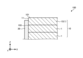
- Fig. 1A is a perspective view showing an example of a wiring board according to a first embodiment.
- Fig. 1B is a cross-sectional view taken along line A-A in Fig. 1A.
- a wiring board 100 according to the first embodiment has an insulating base 10 and a conductor layer 20.
- the insulating base 10 has a plurality of ceramic insulating layers 1.
- the insulating base 10 has a structure in which a plurality of ceramic insulating layers 1 are integrated.
- the insulating base 10 has a first surface 101 and a second surface 102 located at both ends in the thickness direction (Z-axis direction).
- FIG. 1B shows an example in which the insulating base 10 has seven ceramic insulating layers 1, there is no limit to the number of ceramic insulating layers 1 that the insulating base 10 has.
- the ceramic insulating layer 1 may be, for example, a glass ceramic.
- glass ceramic may be any of the following: a composite of a glass phase and ceramic particles, a composite of a glass phase and a crystalline phase formed by the crystallization of a part of the glass phase, a form in which ceramic particles exist in a glass phase, and a form in which a glass phase exists at the grain boundaries between ceramic particles.
- the ceramic insulating layer 1 may be, for example, a ceramic composition that can be co-fired with copper, as described below.
- the conductor layers 20 are located between the laminated ceramic insulating layers 1.
- the conductor layers 20 may be located on the first surface 101 and/or the second surface 102, which are the surfaces of the insulating substrate 10.
- the conductor layers 20 may be formed, for example, by firing a conductor paste containing copper powder.
- the conductor layers 20 may be a copper metallized film.
- the insulating base 10 also has a coating film 30.
- the coating film 30 is inorganic. In this case, the coating film 30 is located on the peripheral portion 103AA of the insulating base 10, which will be described later.
- the coating film 30 only needs to be located on at least the side surface 103 of the insulating base 10, which is located between the first surface 101 and the second surface 102.
- FIG. 2A is a perspective view showing an example of a ceramic insulating layer of the wiring board according to the first embodiment.
- FIG. 2B is a cross-sectional view taken along line B-B of FIG. 2A.
- FIG. 2B corresponds to an illustration of region R1 shown in FIG. 1B.
- the peripheral portion 103AA of the insulating base 10 refers to the portion including the side surface 103 of the insulating base 10 and extending from this side surface 103 to the space between adjacent ceramic insulating layers 1 in the stacking direction of the insulating base 10.
- the portion of the insulating base 10 that extends between adjacent ceramic insulating layers 1 in the stacking direction is referred to as the peripheral region 103A.
- the peripheral portion 103AA is the combined portion of the side surface 103 and the peripheral region 103A in the insulating base 10.
- the wiring board 100 can improve its thermal shock resistance. For example, cracks are less likely to occur on the side surface 103 of the insulating base 10 and in its vicinity. In addition, partial peeling is less likely to occur between the two overlapping ceramic insulating layers 1.
- the coating film 30 may be positioned so as to cover the entire layer of the ceramic insulating layer 1 exposed on the side surface 103 of the insulating base 10.
- the coating film 30 mainly covers the so-called end surface portion of the ceramic insulating layer 1 exposed on the side surface 103 of the insulating base 10. In this case, it is possible to further improve the thermal shock resistance of the wiring board 100.
- cracks are less likely to occur on the side surface 103 of the insulating base 10 and in the vicinity thereof.
- partial peeling of the two layers is less likely to occur in the area between the two overlapping ceramic insulating layers 1.
- the coating film 30 used in the wiring board 100 is made of an inorganic material. Because the material of the coating film 30 is inorganic, it has a high affinity with the insulating base 10 and the ceramic insulating layer 1. It is preferable that the coating film 30 is sintered and integrated with the insulating base 10 and the ceramic insulating layer 1. It is preferable that the coating film 30 and the insulating base 10 are integrated to the extent that no linear interface is discernible. It is also preferable that the coating film 30 and each ceramic insulating layer 1 are integrated to the extent that no linear interface is discernible.
- the coating film 30 and the ceramic insulating layer 1 preferably contain a metal oxide containing Si, such as silica.
- the coating film 30 and the ceramic insulating layer 1 are preferably in a liquid phase sintered state between them.
- the configuration shown in Figures 1A and 1B can be obtained, for example, by the following method.
- a plurality of such pattern sheets are stacked to form a laminate.
- glass slurry that will become the coating film 30 is applied to the side of the laminate.
- a method of immersing the side of the laminate in glass slurry stored in a container may also be used.
- the laminate to which the glass slurry has been applied is fired.
- Delamination is likely to occur in the wiring board 100 because when a conductor pattern is formed on the surface of a green sheet, the pattern sheet has a step equal to the thickness of the conductor pattern when the surface of the green sheet is used as a reference.
- This conductor pattern is formed on the surface of the green sheet, excluding the peripheral region. In the peripheral region of the green sheet, a step occurs due to the thickness of the conductor pattern. When multiple pattern sheets, which originally have a step due to the thickness of the conductor pattern, are stacked, the steps of each pattern sheet accumulate in the laminate.
- the green sheets that make up the pattern sheets contain an organic binder. This makes the green sheets thermoplastic, and they deform during the pressure and heat treatment that is used to create the laminate. The green sheets, by their own deformation, fill in the gaps caused by the thickness of the conductor patterns. However, when a large number of pattern sheets are stacked, the bonds between the green sheets near the sides of the laminate may become weak.
- the delamination and cracks that occur in the wiring board 100 are caused by stresses that arise due to differences in the thermal expansion coefficient and Young's modulus that are based on differences in the materials between the ceramic insulating layer 1 and the conductor layer 20.
- the stress generated between the ceramic insulating layer 1 and the conductor layer 20 is said to be likely to concentrate on the periphery of the conductor layer 20 in the wiring board 100. Since delamination is a behavior that occurs between two overlapping ceramic insulating layers 1, the side of the wiring board 100 or the insulating base 10, which is the open end of the wiring board 100, becomes the source of destruction.
- the wiring board 100 of the present disclosure has a coating film 30 integrally formed on the peripheral portion 103AA from the same material as the insulating base 10. This reduces the possibility that the side of the wiring board 100 or insulating base 10, which is the open end of the wiring board 100, will become a source of destruction.
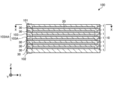
- Second Embodiment Fig. 3 is a cross-sectional view showing an example of a wiring board according to the second embodiment Fig. 4 is an enlarged view showing a part of the wiring board shown in Fig. 3 .
- the insulating base 10 may have exposed portions 11, 12 on the side of the ceramic insulating layer 1 located on the outermost layer, where the coating film 30 is not located.
- the exposed portions 11, 12 are the portions of the side 103 of the insulating base 10 where the coating film 30 is not adhered.
- the exposed portion 11 may be located on the first surface 101 side, which is the main surface, of the ceramic insulating layer 1S located at the end on the positive side of the Z axis. This makes it difficult for the flatness of the first surface 101 to decrease. Therefore, it is possible to position the conductor layer 20 up to the periphery of the first surface 101, for example.
- the exposed portion 12 may be located on the second surface 102 side, which is the main surface, of the ceramic insulating layer 1 located at the end on the negative side of the Z axis. This makes it difficult for the flatness of the second surface 102 to decrease. Therefore, it is possible to position the conductor layer 20 up to the periphery of the second surface 102, for example.
- the configuration shown in FIG. 3 can be produced, for example, by dipping a laminate in which ceramic insulating layers 1 are stacked, using glass slurry, which is the material of the coating film 30.
- the exposed portions 11 and 12 of the laminate, where the coating film 30 is not formed, are masked with tape or the like to prevent the glass slurry from adhering thereto.
- the tape should be removed before degreasing and firing.
- the insulating base 10 may have only one of the exposed portions 11 and 12.
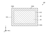
- Fig. 5 is a plan view showing an example of a wiring board according to the third embodiment
- Fig. 6 is a cross-sectional view showing an example of a wiring board according to the third embodiment.
- the coating film 30 may be positioned so as to surround the entire periphery of the side surface 103 of the insulating base 10. This makes it less likely that peeling or cracking will occur in the ceramic insulating layer 1 around the entire periphery of the side surface 103 of the wiring board 100.
- the thickness of the coating film 30 covering the corner 103c where the side surfaces 103 of adjacent insulating substrates 10 intersect may be smaller than the thickness of the coating film 30 located on the side surfaces 103 excluding the corner 103c.
- the corner portion 31 of the coating film 30 covering the corner 103c may have a rounded outline.
- the corners 103c are more likely to chip when they come into contact with other structures than the sides (or edges) between the two corners 103c. However, if the thickness of the coating film 30 at the corners 103c is made thinner than that of the sides (or edges), the coating film 30 at the corners 103c is less likely to chip, and damage to the aesthetic appearance of the product can be reduced.
- the coating film 30 may have a shape in which the thickness of the end 32 closest to the first surface 101 gradually decreases as it approaches the first surface 101. Also, the end 32 of the coating film 30 may be rounded.
- the shape of the coating film 30 in the Z direction (up and down direction) of the insulating base 10 is also better if it is rounded rather than angular. In this case too, the coating film 30 is less likely to chip, making it easier to maintain the aesthetic appearance of the wiring board 100.
- FIG. 7 is a plan view showing an example of a wiring board according to the fourth embodiment.
- the insulating base 10 may have rounded corners 103c located between adjacent side surfaces 103.
- the coating film 30 may be located on the side surface 103 of the insulating base 10 excluding the rounded corners 103c. This makes it difficult for the insulating base 10 to be chipped at the corners 103c due to the coating film 30.
- FIG. 8 is a plan view showing an example of a method for manufacturing the wiring board shown in FIG. 7.
- the plan view shown in FIG. 8 shows the green laminate 50.
- This green laminate 50 is sized to be able to produce multiple insulating bases 10 that form the basis of the wiring board 100 described above.
- the green laminate 50 shown in FIG. 8 is sized to be able to produce four wiring boards 100 (or insulating bases 10).
- the green laminate 50 is a laminate that can be produced in multiple pieces, not limited to four.
- a green laminate 50 having such a shape is prepared.
- a plurality of through holes 51-54 are provided in the green laminate 50, penetrating it in the thickness direction (Z-axis direction). As shown in FIG. 8, the through holes 51-54 are formed so that the laminates cut out from the green laminate 50 do not fall apart.
- the laminates referred to here correspond to the insulating base 10.
- the through holes 51-54 are processed so that the corners of adjacent laminates (later insulating base 10) in the green laminate 50 can be kept connected.
- the wiring board 100 shown in FIG. 7 may be produced by any method, not limited to the method shown in FIG. 8.
- the green laminate 50 is cut to obtain multiple laminates, and then the multiple laminates are placed in a separately prepared frame, and then glass slurry is poured in. In this case, the multiple laminates are placed at a predetermined interval within the frame.
- an example of the frame structure can be a shape in which the parts of the laminate shown by the dashed lines and the parts corresponding to the through holes 51 to 54 shown by the thick solid rectangles are hollowed out from the rectangular plan view of the green laminate 50 shown in Figure 8.
- Fig. 9 is a cross-sectional view showing an example of a wiring board according to a fifth embodiment.
- Fig. 10 is a cross-sectional view taken along the line X-X of Fig. 9.
- Fig. 10 shows a plan view perspective of the surface of the conductor layer 20 located below the uppermost ceramic insulating layer 1 when the wiring board 100 shown in Fig. 9 is viewed from above (the Z positive direction side).
- the peripheral region 103A of the present disclosure is a frame-shaped portion corresponding to the arrangement of the coating film 30 shown in Fig. 10.
- the coating film 30 may be located in the peripheral portion 103AA of the insulating base 10, between two ceramic insulating layers 1 adjacent to each other in the stacking direction. This makes the wiring board 100 less susceptible to peeling or cracking of the ceramic insulating layer 1 on the insulating base 10.
- the peripheral portion 103AA is a range that includes the peripheral region 103A of each ceramic insulating layer 1 that constitutes the insulating base 10.
- the coating film 30 has a thickness equivalent to the thickness of the conductor layer 20 formed on the ceramic insulating layer 1, and it is sufficient that the coating film 30 is thick enough to eliminate any steps in the conductor layer 20.
- Figures 9 and 10 show a state in which the coating film 30 and the conductor layer 20 are spaced apart at a predetermined distance on the surface of the ceramic insulating layer 1, the present disclosure is not limited to this, and the coating film 30 and the conductor layer 20 may be in contact. Furthermore, when the coating film 30 and the conductor layer 20 are spaced apart on the surface of the ceramic insulating layer 1, it is preferable that a portion of the ceramic insulating layer 1 fills the gap between the coating film 30 and the conductor layer 20 to form a dense state. This can increase the mechanical strength of the insulating base 10.
- the coating film 30 may be located in the peripheral region 103A of the ceramic insulating layer 1 that constitutes the insulating base 10.
- the coating film 30 may be located so as to surround the peripheral region 103A of the ceramic insulating layer 1 that constitutes the insulating base 10. This makes it difficult for the insulating base 10 to peel off between the two overlapping ceramic insulating layers 1 of the wiring board 100. Furthermore, with this configuration, cracks are even less likely to occur in the insulating base 10 and each ceramic insulating layer 1.
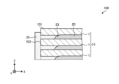
- FIG. 11 is a cross-sectional view showing an example of a wiring board according to the sixth embodiment.
- the conductor layer 20 may have an end 23 whose thickness gradually decreases toward the side surface 103 of the insulating base 10.
- the coating film 30 may have a portion 33 overlapping the conductor layer 20 in the thickness direction. This makes it difficult for the end 23 of the conductor layer 20 to peel off from the ceramic insulating layer 1.
- the coating film 30 may not reach the side surface 103 of the insulating base 10 and may not be exposed on said side surface 103.
- part of the ceramic insulating layer 1 on the side surface 103 of the insulating base 10 integrally connects each layer in the stacking direction, and the side surface 103 of the insulating base 10 plays a role in protecting the coating film 30 located inside the insulating base 10. In this way, it is possible to obtain a wiring board 100 (or insulating base 10) with high mechanical strength.
- Fig. 12 is a cross-sectional view showing an example of a wiring board according to the seventh embodiment.
- the coating film 30 may extend inward from a portion along the side surface 103 of the insulating base 10. This increases the contact area between the coating film 30 and the insulating base 10, making it difficult for peeling of the ceramic insulating layer 1 to occur.
- the coating film 30 shown in FIG. 12 has a structure that is continuous and integrated from the side surface 103 of the insulating base 10 to the ceramic insulating layer 1.
- the coating film 30 has a comb-tooth structure (shape) when the insulating base 10 is viewed in vertical cross section.
- the coating film 30 is connected to the insulating base 10 in the stacking direction and is integrated, thereby increasing the mechanical strength of the coating film 30 itself.
- the coating film 30 has a structure of this shape, the adhesive strength of the coating film 30 to the side surface 103 of the insulating base 10 is increased. Furthermore, the coating film 30 can be firmly adhered to the insulating base 10 over the entire peripheral portion 103AA, which is the combination of the side surface 103 and the peripheral region 103A of the insulating base 10.
- Fig. 13 is a cross-sectional view showing an example of a wiring board according to the eighth embodiment.
- the coating film 30 shown in Fig. 13 has a smaller volume of the portion provided on the side surface 103 of the insulating base 10 than the coating film 30 shown in Fig. 12.
- the coating film 30 located on the side surface 103 may not be connected in the stacking direction and may cover a part of the end surface of each ceramic insulating layer 1.
- the thickness and volume of the side surface 103 of the coating film 30 are reduced, which contributes to reducing the volume and weight of the wiring board 100. In this case, too, peeling between the two laminated ceramic insulating layers 1 in the insulating base 10 can be prevented, and the possibility of cracks occurring in the ceramic insulating layer 1 can be reduced.
- the coating film 30 is in contact with the end 23 of the conductor layer 20, but the conductor layer 20 and the coating film 30 may be partially separated. In this case, it is preferable that the ceramic insulating layer 1 partially fills the gap between the conductor layer 20 and the coating film 30. This can reduce the decrease in density of the insulating base 10.
- glass ceramics can be used as a suitable material for the ceramic insulating layer 1. Therefore, a glassy material is more suitable for the material of the coating film 30. This allows the material of the coating film 30 to have a lower Young's modulus than the material of the ceramic insulating layer 1. For example, when the wiring board 100 (insulating base 10) is subjected to an external force, the coating film 30 acts as a buffer material, making the wiring board 100 less likely to be damaged.
- the Young's modulus of the material of the coating film 30 is lower than that of the material of the insulating base 10 or the ceramic insulating layer 1, in consideration of the situation in which the coating film 30 is in contact with both the conductor layer 20 and the ceramic insulating layer 1, there is a high possibility that the stress generated between the conductor layer 20 and the ceramic insulating layer 1 will be further alleviated.
- the glass ceramics that is the material of the ceramic insulating layer 1 may contain inorganic filler.
- the coating film 30 may not contain inorganic filler.
- inorganic filler refers to, for example, a particulate inorganic material with a maximum diameter of 3 ⁇ m or more.
- the insulating base 10 may be a glass ceramic containing a filler.
- the coating film 30 may have a smaller filler content than the insulating base 10.
- the coating film 30 may have a lower softening point than the ceramic insulating layer 1.
- the softening points of the coating film 30 and the ceramic insulating layer 1 can be measured by the DSC method. This indicates the characteristics (softening point) of the solid content of the glass slurry used to form the coating film 30.
- the softening point of the solids contained in the glass slurry applied to the laminate and green sheet when forming the insulating base 10 is lower than the softening point of the solids contained in the green sheet, the glass slurry that becomes the coating film 30 will sinter at a lower temperature than the laminate (green sheet) when firing the laminate.
- the peripheral portion 103AA of the insulating base 10 will be subjected to a restraining force by the coating film 30 based on the glass slurry during sintering.
- the peripheral portion 103AA of the insulating base 10 (or wiring board 100) is less likely to change in shape, such as becoming distorted, during firing.
- a green sheet (100 mm x 100 mm x 200 ⁇ m thick) containing glass ceramic raw material powder was prepared.
- the glass ceramic raw material powder was a mixed powder of borosilicate glass and silica particles. Specifically, a mixed powder was used in which 50 parts by mass of silica particles were added to 100 parts by mass of borosilicate glass.
- a butyral-based organic resin was used as the organic vehicle for the green sheet.
- the conductive paste that becomes the conductive layer is a mixture of copper powder and borosilicate glass powder.
- a cellulose-based organic resin is used as the organic vehicle.
- the solid content is 100 parts by mass of copper powder and 30 parts by mass of borosilicate glass powder.
- a glass paste was prepared for forming the coating film.
- a cellulose-based organic resin was used as the organic vehicle.
- the softening point of the glass powder used in the glass paste was 500°C.
- the softening point of the glass powder used in the green sheet was 700°C. If the softening points are the same, the softening point may be changed depending on whether or not an inorganic filler is used.
- a conductor pattern (representation before firing) was formed by printing a conductor paste in a solid manner in the central area of the green sheet, leaving a peripheral area (3 mm) remaining.
- the thickness of the conductor pattern was approximately 20 ⁇ m.
- a glass paste was printed on the peripheral portion of the green sheet on which the conductor pattern was formed to produce a pattern sheet with a glass pattern.
- the thickness of the glass pattern was the same as that of the conductor pattern.
- the thickness of the ends of the conductor pattern tended to become gradually thinner.
- Two types of glass patterns were produced: one that did not overlap the conductor pattern (see, for example, Figure 9) and one that overlapped (see, for example, Figure 11).
- a blank green sheet with no conductor or glass pattern was placed on top and pressurized and heated (30 MPa, 100°C, 10 minutes) to create a laminate.
- the size of the laminate was approximately 100 mm x 100 mm x 7 mm. After degreasing in a moist nitrogen atmosphere, the laminate was fired in a dry nitrogen atmosphere at a maximum temperature of 950°C for 2 hours.
- ten samples were also produced by creating a laminate using a pattern sheet on which no glass paste was printed, and coating the sides of the laminate with glass paste (glass coating was performed by immersing the edges of the laminate in glass slurry contained in a container). Protective tape was partially attached to the main surface of the outermost green sheet to prevent the glass paste from adhering to it.
- the glass paste coating film was shaped so that it gradually became thinner at the ends corresponding to the corners of the laminate (insulating base).
- a comparative example ten samples of similar size were produced in which glass paste was not printed on the peripheral portion of the insulator (sample 1).
- a wiring board of 10 mm x 10 mm (same thickness) was produced in the same manner in which glass paste was not printed (sample 2).
- the area ratio of the conductor pattern to the area of the green sheet was the same as in the case of 100 mm x 100 mm.
- sample 4 showed no peeling (delamination) on the sides of the wiring board, even in a heat resistance test in which the wiring board sample was immersed in a solder bath heated to 330°C for one second. Furthermore, no cracks were found in the ceramic insulating layer of sample 4.
- sample 3 in which the glass pattern does not overlap the conductor pattern, delamination was observed in one out of ten samples in a solder heat resistance test under the same conditions.
- sample 3 in the wiring board in which delamination was observed, cracks were observed in part of the ceramic insulation layer of the wiring board.
- the wiring board includes an insulating base in which a plurality of ceramic insulating layers are laminated and integrated, A conductor layer;
- the insulating base has an inorganic coating film on the periphery of the insulating base.
- the coating film may be located on a side surface of the insulating base.
- the coating film may be positioned so as to cover the entire side surface of the insulating base.
- the insulating base may have an exposed portion on the main surface of the side of the ceramic insulating layer located in the outermost layer, where the coating film is not located.
- the coating film may be positioned so as to surround the entire periphery of the side surface of the insulating base.
- the insulating base has rounded corners located between adjacent side surfaces,
- the coating film may be located on a side surface of the insulating base excluding the corner portions.
- the coating film may be located in the peripheral portion between two ceramic insulating layers adjacent to each other in the stacking direction.
- the average thickness of the coating film may be smaller than the average thickness of the conductor layer.
- the conductor layer has an end portion whose thickness gradually decreases toward a periphery of the insulating base,
- the coating film may have a portion overlapping the conductor layer in a thickness direction.
- the material of the ceramic insulating layer is glass ceramics,
- the material of the coating film may be glass.
- the insulating base is a glass ceramic containing a filler
- the coating film may have a smaller filler content than the insulating base.
- the coating film may have a softening point lower than that of the ceramic insulating layer.
- the coating film may extend inward from a portion along the side of the insulating base.
- the coating film may be positioned so as to extend from between the layers of the insulating base to the side of the insulating base.
Landscapes
- Engineering & Computer Science (AREA)
- Microelectronics & Electronic Packaging (AREA)
- Manufacturing & Machinery (AREA)
- Production Of Multi-Layered Print Wiring Board (AREA)
- Non-Metallic Protective Coatings For Printed Circuits (AREA)
- Laminated Bodies (AREA)
Priority Applications (1)
| Application Number | Priority Date | Filing Date | Title |
|---|---|---|---|
| JP2025516848A JPWO2024225318A1 (https=) | 2023-04-26 | 2024-04-24 |
Applications Claiming Priority (2)
| Application Number | Priority Date | Filing Date | Title |
|---|---|---|---|
| JP2023-072537 | 2023-04-26 | ||
| JP2023072537 | 2023-04-26 |
Publications (1)
| Publication Number | Publication Date |
|---|---|
| WO2024225318A1 true WO2024225318A1 (ja) | 2024-10-31 |
Family
ID=93256646
Family Applications (1)
| Application Number | Title | Priority Date | Filing Date |
|---|---|---|---|
| PCT/JP2024/016078 Ceased WO2024225318A1 (ja) | 2023-04-26 | 2024-04-24 | 配線基板 |
Country Status (3)
| Country | Link |
|---|---|
| JP (1) | JPWO2024225318A1 (https=) |
| TW (1) | TWI908043B (https=) |
| WO (1) | WO2024225318A1 (https=) |
Citations (6)
| Publication number | Priority date | Publication date | Assignee | Title |
|---|---|---|---|---|
| JP2008078454A (ja) * | 2006-09-22 | 2008-04-03 | Murata Mfg Co Ltd | 多層セラミック基板およびその製造方法 |
| JP2010153558A (ja) * | 2008-12-25 | 2010-07-08 | Kyocera Corp | 配線基板及び配線基板の製造方法 |
| JP2016174084A (ja) * | 2015-03-17 | 2016-09-29 | 京セラ株式会社 | 素子搭載用基板および実装基板 |
| WO2016152990A1 (ja) * | 2015-03-25 | 2016-09-29 | 京セラ株式会社 | 電子部品 |
| CN209030459U (zh) * | 2018-08-31 | 2019-06-25 | 深圳市瑞博兴源电子有限公司 | 一种耐热型电路板 |
| WO2020022109A1 (ja) * | 2018-07-25 | 2020-01-30 | 株式会社村田製作所 | 複合基板及び複合基板の製造方法 |
Family Cites Families (1)
| Publication number | Priority date | Publication date | Assignee | Title |
|---|---|---|---|---|
| JP2013157496A (ja) * | 2012-01-31 | 2013-08-15 | Sony Corp | 発光素子およびその製造方法、並びに発光装置 |
-
2024
- 2024-04-24 JP JP2025516848A patent/JPWO2024225318A1/ja active Pending
- 2024-04-24 WO PCT/JP2024/016078 patent/WO2024225318A1/ja not_active Ceased
- 2024-04-26 TW TW113115619A patent/TWI908043B/zh active
Patent Citations (6)
| Publication number | Priority date | Publication date | Assignee | Title |
|---|---|---|---|---|
| JP2008078454A (ja) * | 2006-09-22 | 2008-04-03 | Murata Mfg Co Ltd | 多層セラミック基板およびその製造方法 |
| JP2010153558A (ja) * | 2008-12-25 | 2010-07-08 | Kyocera Corp | 配線基板及び配線基板の製造方法 |
| JP2016174084A (ja) * | 2015-03-17 | 2016-09-29 | 京セラ株式会社 | 素子搭載用基板および実装基板 |
| WO2016152990A1 (ja) * | 2015-03-25 | 2016-09-29 | 京セラ株式会社 | 電子部品 |
| WO2020022109A1 (ja) * | 2018-07-25 | 2020-01-30 | 株式会社村田製作所 | 複合基板及び複合基板の製造方法 |
| CN209030459U (zh) * | 2018-08-31 | 2019-06-25 | 深圳市瑞博兴源电子有限公司 | 一种耐热型电路板 |
Also Published As
| Publication number | Publication date |
|---|---|
| TW202508375A (zh) | 2025-02-16 |
| TWI908043B (zh) | 2025-12-11 |
| JPWO2024225318A1 (https=) | 2024-10-31 |
Similar Documents
| Publication | Publication Date | Title |
|---|---|---|
| US11011307B2 (en) | Electronic component | |
| US6036798A (en) | Process for producing electronic part with laminated substrates | |
| KR102721789B1 (ko) | 적층 세라믹 콘덴서 | |
| KR102710047B1 (ko) | 적층 세라믹 콘덴서 | |
| JP5182367B2 (ja) | 多層セラミック基板およびその製造方法 | |
| CN117079971A (zh) | 层叠陶瓷电容器 | |
| JP4099756B2 (ja) | 積層基板 | |
| JP2003022929A (ja) | 積層セラミックコンデンサ | |
| US6621010B2 (en) | Multilayer integrated substrate and manufacturing method for multilayer ceramic element | |
| JP4788544B2 (ja) | 多層セラミック基板およびその製造方法 | |
| WO2024225318A1 (ja) | 配線基板 | |
| CN113555220B (zh) | 层叠陶瓷电容器 | |
| US20230113966A1 (en) | Electronic component and method for manufacturing electronic component | |
| JP2001144437A (ja) | 多層セラミック基板およびその製造方法 | |
| JPH067578B2 (ja) | セラミツク多層基板 | |
| KR100992238B1 (ko) | 무수축 세라믹 기판의 제조 방법 | |
| JP2003273515A (ja) | セラミックの低温焼結の間の収縮を低減するための方法および抑制層 | |
| KR100835080B1 (ko) | 적층 세라믹 기판 제조방법 | |
| JP2001160683A (ja) | 多層セラミック基板およびその製造方法 | |
| KR100872297B1 (ko) | 다층 세라믹 기판의 제조 방법 | |
| JPH11233944A (ja) | セラミック多層基板の製造方法 | |
| WO2025070020A1 (ja) | 配線基板の製造方法 | |
| KR100887112B1 (ko) | 무수축 세라믹 기판의 제조방법 및 이에 의해 제조된 다층세라믹 기판 | |
| WO2023238807A1 (ja) | 積層セラミック電子部品および積層セラミック電子部品の製造方法 | |
| JP4507705B2 (ja) | セラミック基板の製造方法および未焼結複合積層体 |
Legal Events
| Date | Code | Title | Description |
|---|---|---|---|
| 121 | Ep: the epo has been informed by wipo that ep was designated in this application |
Ref document number: 24797064 Country of ref document: EP Kind code of ref document: A1 |
|
| ENP | Entry into the national phase |
Ref document number: 2025516848 Country of ref document: JP Kind code of ref document: A |
|
| WWE | Wipo information: entry into national phase |
Ref document number: 2025516848 Country of ref document: JP |
|
| NENP | Non-entry into the national phase |
Ref country code: DE |
|
| 122 | Ep: pct application non-entry in european phase |
Ref document number: 24797064 Country of ref document: EP Kind code of ref document: A1 |